
Abstract
The present paper presents a systematic investigation of both catalyst free and catalyst assisted AlN nanowire synthesis by chemical vapour deposition using Al and NH3 as source materials. Growth runs have mostly been carried out at 1100°C under H2 as carrier gas. While the catalyst free growth runs resulted in long (∼40 μm) and dense AlN nanowire array films, the catalyst assisted growth resulted in short nanowires (3–5 μm). Growth mechanisms have been presented. Raman spectroscopy of the catalyst free grown nanowires has revealed very symmetric and strong phonon modes [e.g. strong E2 (high)] indicating very good crystal quality of the grown AlN nanowires. In brief, catalyst free growth eliminates catalyst contamination and produces high quality and density of long nanowires, which is very valuable for scale-up manufacturing opportunities of the AlN nanostructures.
Introduction
III–V nitride semiconductor materials have stimulated great research and technological interests due to their unique properties for many applications in microelectronics and optoelectronics. Aluminium nitride (AlN), one of the important wide band gap III–V semiconductors, possesses excellent thermal conductivity, low thermal expansion coefficient, high chemical stability and high electrical resistivity.1–3 Moreover, one-dimensional AlN (1D-AlN) nanostructures combine these unique inherent properties with low dimensional advantages and offer superior performances for potential applications in several fields including power transistors, heat sinks, surface acoustic wave applications, UV optoelectronics, piezoelectric nanogenerators and spintronics.4–6 Additionally, 1D-AlN nanostructures with high aspect ratios have very promising applications in field emission devices due to very low electron affinity. 7
Owing to these very promising applications, significant research has been devoted to the synthesis of 1D-AlN nanostructures with various fabrication methods. These fabrication methods include metal organic vapour deposition, 8 arc discharging process, 9 chloride assisted growth, 10 carbothermal reduction, 11 gas reduction nitridation 12 and chemical vapour deposition (CVD).13–20 Nevertheless, most of these fabrication methods involve the use of catalysts (mostly Au), which can introduce detrimental defects in AlN resulting poor performances in electronic and optoelectronic applications. Another significant problem with many earlier efforts can be stated as producing short length ( < 2 μm) AlN nanostructures, which makes it very difficult to manipulate and integrate them for nanodevice fabrication.
The present paper presents a systematic investigation of both catalyst free and catalyst assisted AlN nanowire synthesis by CVD using Al and NH3 as source materials, and physical properties of these AlN nanostructures. The catalyst free AlN nanostructures have directly been fabricated on the alumina boat without any substrate. Additionally, no hazardous gases or precursors (e.g. chlorine based gases) have been used for the growth process. This very simple, safe and efficient fabrication approach has resulted in very high quality and dense AlN nanowire array films. In attempts to compare with catalyst assisted growth, studies with various catalyst materials have also been presented (Co, Au, Ni and Fe). Both the catalyst free and catalyst assisted growth mechanisms have been discussed. As a consequence, free standing and catalyst free AlN nanowire films provide great opportunities due to enabling easy transfer of these into any substrate for the development of new devices for many scientific and technological applications.
Experimental
AlN nanowire growth has taken place in a resistively heated hot wall 25 mm horizontal low pressure CVD reactor. Si and SiO2/Si substrates were used for the catalyst assisted growth. SiO2 (400 nm thick) was formed by thermal oxidation of Si wafer. Various catalyst materials including Ni (20 nm size nanoparticle and thin film), Au of 20 nm, Fe of 40 nm and Co of 25 nm were used. All the catalyst materials have been placed on SiO2/Si substrate except Ni film, which was predeposited on Si substrate by sputtering. The substrate was ultrasonically cleaned in acetone, isopropyl alcohol and deionised water and dried with nitrogen. Nanoparticle solution was applied to the substrate surface and dried. An alumina boat containing both the substrate and Al (99·97 purity, ∼30 mg) was loaded into the CVD reactor. For catalyst free growth runs, Al (∼30 mg) was directly placed into the alumina boat without any substrate. Moreover, the growth has directly taken place on top of the Al source. Following loading, the reactor was evacuated and purged three times with hydrogen (99·999). After purging cycles, the reactor was heated to the growth temperature (mostly at 1100°C, unless specified for a different temperature) under hydrogen. Then, the growth was carried out by flowing NH3 (99·99) and H2 gases through the reactor. The growth times for the catalyst assisted and catalyst free growth were 15–30 min and 2 h respectively. The gas flowrates were controlled by mass flow controllers and set to 300 standard cubic centimetres per minute for both H2 and NH3. After the growth, NH3 was shut off, and the reactor was cooled down under H2 flow until 250°C. Then, the furnace cooled down to room temperature.
The grown samples have been characterised by scanning electron microscopy (SEM) (JEOL JSM 6060 and JEOL 7600F SEM with Oxford Inca energy dispersive X-ray spectroscopy (EDS)), Raman spectroscopy (Renishaw inVia Raman microscope with 532 nm laser excitation wavelength and Leica DMLM microscope), X-ray diffraction (XRD) (Rigaku 300 and Bruker D8 Discover) and transmission electron microscopy (TEM) (JEOL JEM 1011).
Results and discussion
Figure 1 shows SEM images of the AlN nanowires grown on 20 nm Ni coated Si and SiO2/Si with 25 nm Co nanoparticles at 1100°C under H2 as carrier gas. The AlN nanowire diameters grown on Ni film are in the range of 20 to 30 nm and lengths about few micrometres. It is worth mentioning that the metal catalysts were observed at the end of the nanowires. This observation indicates that AlN nanowire growth has taken place via vapour–liquid–solid (VLS) growth mechanism. 21 In the VLS mechanism, the metal droplet acts as a catalyst for decomposing the crystalline constituents. As the constituents for nanostructures become supersaturated within the liquid solution, crystal growth proceeds by precipitation of source materials from the solid/liquid interface. In general, the VLS mechanism results in highly anisotropic nanostructures, since nucleation and growth process is mainly controlled by the liquid catalyst droplet. The AlN nanowire diameters grown with Co nanoparticles are in the range of 25–35 nm and lengths about several micrometres. Majority of the AlN nanowires grown with Co have kink morphologies. The growth runs have been repeated at the same conditions with different catalyst materials including Fe and Au. Nevertheless, Fe or Au catalysts did not yield any nanowire growth. Following that, AlN growth was carried out at different temperatures with the most active catalysts (Ni and Co). In the temperature range of 800–950°C, no nanowire growth was observed. AlN nanowires appeared at 1000°C, and the nanowire growth yield has increased with temperature and reached its peak at 1100°C.
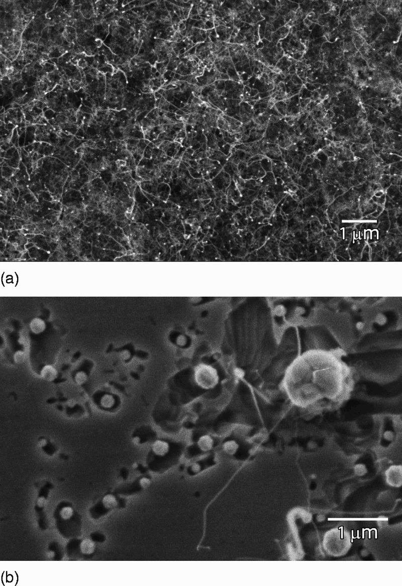
a Ni film; b Co nanoparticle solution
Next, the efforts have been focused on the catalyst free growth to eliminate the catalyst contamination. Figure 2 exhibits SEM images of the catalyst free grown ultradense AlN nanostructure films at 1100°C. The AlN nanostructures were grown on the source Al, which was placed directly to the alumina boat without any substrate. The image also displays quasi-aligned AlN nanowires in clusters distributed over the alumina boat. The AlN nanowire tip diameters are ∼30 nm and lengths up to 10 μm. The growth takes place in clusters resembling a multiprong growth through a VLS mechanism with Al droplets serving as the self-catalyzing agents, and the proposed growth mechanism is presented in the following paragraph. The self-catalyzing VLS mechanism has previously been reported for various nanostructured materials including ZnO22,23 and AlN.19,20 In order to achieve self-catalysed AlN nanowires, however, Fe2O3 powders 19 or ammonium chloride and nickel nitrate 20 have been added to the growth ambient respectively. It is very important to emphasise that only Al and NH3 have been used as source materials in the present study (i.e. no hazardous gases or precursors have been used for the growth process).
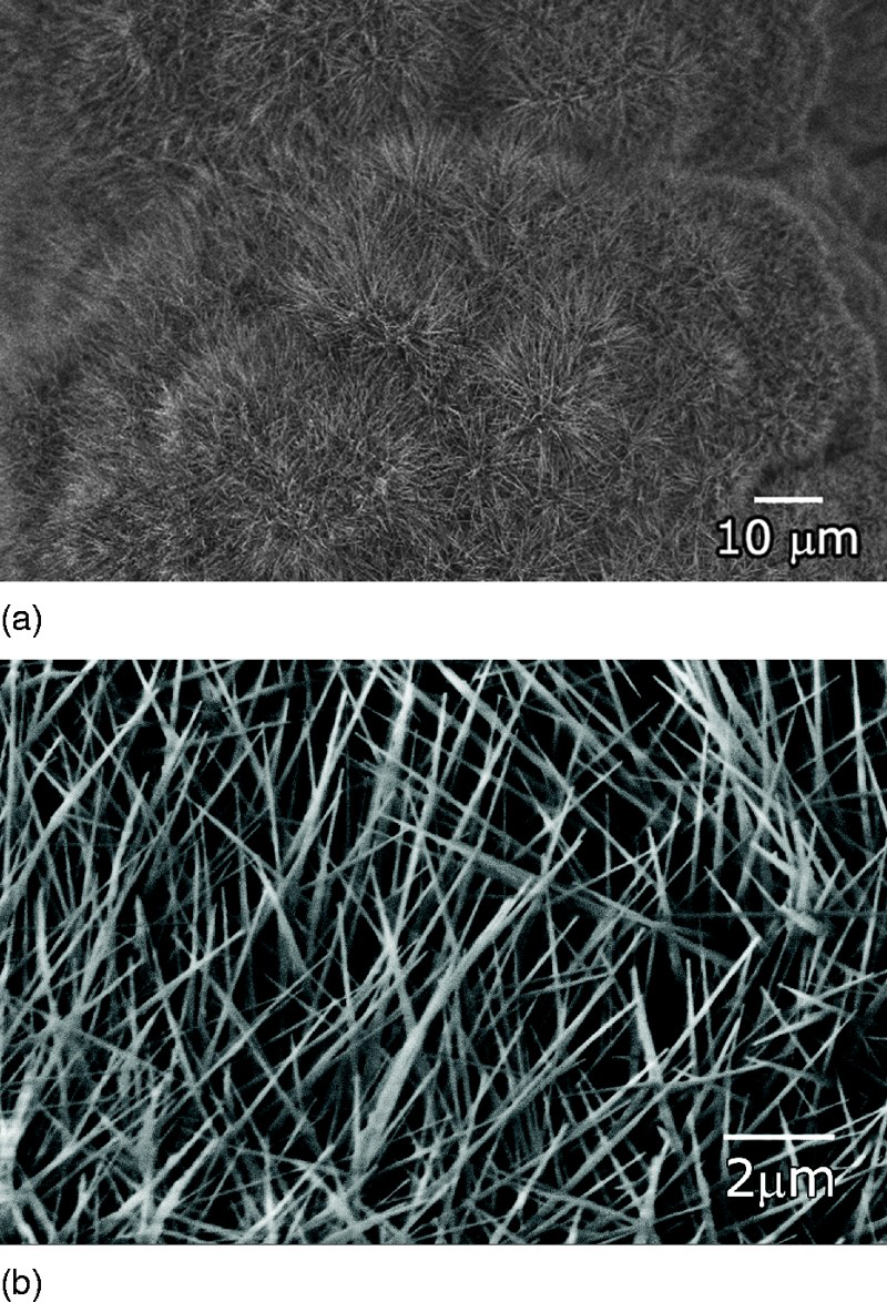
a low magnification (cluster-like multiprong growth); b high magnification (AlN nanowires with 30 nm tip diameter and 7–10 μm length)
The size uniformity of the AlN nanowires suggests very fast and spontaneous nucleation. Moreover, the cluster-like morphology (see Fig. 2a) suggests a high interfacial energy between the alumina boat and the Al droplets.
24
The growth process can be described step by step as follows: first, the Al powders melt and form a film during the heating cycle due to low melting point of Al (650°C). As the temperature approaches to the growth temperature of 1100°C, the Al film gradually breaks and forms clusters and droplets due to the reducing effect of H2 gas25,26 and Ostwald ripening at high temperatures. When the NH3 gas introduced into the reactor, the following reaction takes place

In order to change the wetting morphology of the molten Al source on the boat, which would influence the growth process, a source mixture of Al–Al2O3 was used for several growth runs. The AlN nanostructures were directly grown on the source mixture of Al–Al2O3, which was placed to the alumina boat without any substrate. Figure 3 shows SEM images of the catalyst free grown ultradense AlN nanowire films at 1100°C. These free standing nanostructure films were attached to conductive carbon tape before placing to the SEM sample holder. The AlN nanowire diameters are in the range of 45–65 nm and lengths up to few tens of micrometres. The growth takes place through a VLS growth mechanism with Al droplets serving as the catalyst. Nevertheless, cluster-like multiprong growth has not been observed. This is presumably due to lack of large Al cluster/droplet formation caused by solid Al2O3 powder underneath the molten Al source. Additionally, EDS was used for the chemical analysis of the grown AlN nanowires. The EDS spectrum, shown in Fig. 4, indicates the presence of only Al and N elements. No oxygen was observed. The purity and crystal quality of the grown AlN nanowires have further been verified by XRD, TEM and Raman spectroscopy.
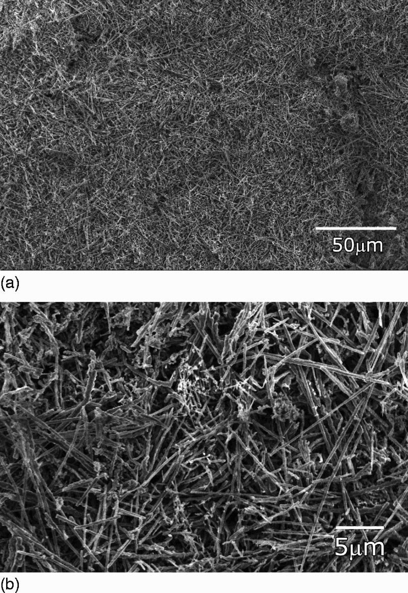
a low magnification; b high magnification (AlN nanowires with 45–65 nm diameter; and lengths up to few tens of micrometres)
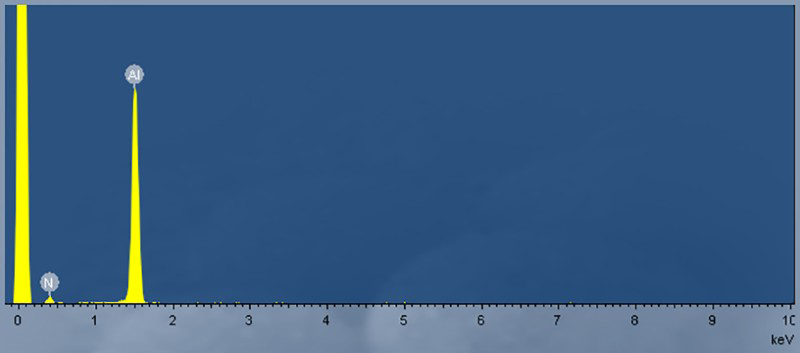
Energy dispersive X-ray spectrum acquired from catalyst free grown AlN nanostructure films
Next, XRD measurements were carried out using Cu Kα radiation (λ = 0·154 nm) to determine the structure and crystal quality of the AlN nanostructures, and a typical spectrum is shown in Fig. 5. The diffraction peaks in the spectrum were indexed to a hexagonal wurtzite crystal structure. The lattice constants derived from the peak positions were a = 0·3114 nm and c = 0·4979 nm (Joint Committee on Powder Diffraction Standards no. 25-1133). The diffraction peaks and their positions from the AlN nanostructures can be listed as: (100), 33·2°; (002), 36·04°; (101), 37·92°; (102), 49·82°; and (110), 59·35°. No characteristic peak associated with other crystalline forms or phases was detected in the XRD spectrum. This suggests that the catalyst free grown AlN nanostructures consist of only one crystalline phase, and the Al source has completely been reacted and consumed. Furthermore, the narrow peaks indicate a narrow range of composition and free of stress of the AlN nanostructures (see Fig. 5).
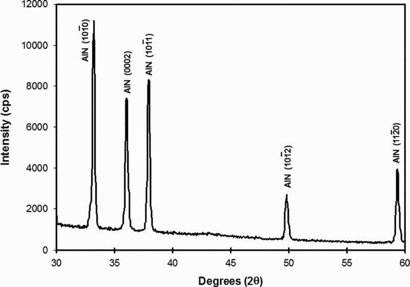
X-ray diffraction pattern of AlN nanostructures indicating hexagonal wurtzite structure
Following the XRD measurements, TEM was performed to further characterise the morphology and diameter of the nanostructures. The TEM specimen was prepared by breaking small pieces from the dense film to the carbon coated copper grids. Figure 6 shows the TEM image of the AlN nanowires with diameters ranging from 45 to 65 nm. Moreover, the diameter of some nanowires gradually decreases along its length towards the tip of the nanowires, as observed by TEM. This tapered morphology suggests that the supply of Al source decreases as the growth progresses.
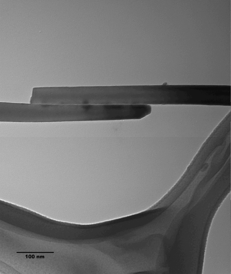
TEM images of catalyst free grown AlN nanowires with 45–65 nm diameter
In attempts to study optical properties of the AlN nanowires, their Raman spectra were recorded using a Renishaw Raman microscope system with 532 nm laser as an excitation source. Raman spectroscopy is a very useful technique to study the optical and crystalline quality of the nanostructured materials. There are six first order Raman active modes of hexagonal AlN, i.e. 1 A1(TO)+1 A1(LO)+1 E1(LO)+1 E1(TO)+2 E2. 27 The Raman spectrum of the catalyst free grown AlN nanowires is shown in Fig. 7. The Raman spectrum yields peaks at 611 cm− 1 (A1; TO), 656 cm− 1 (E2; high), 668·3 cm− 1 (E1; TO) and 907·4 cm− 1 (A1; LO), which agrees well with the high quality single crystalline bulk AlN. 27 The E2 (high) mode is used to analyse the stress state of AlN crystals due to its high sensitivity to stress. 27 It is worth mentioning that the sharp and strong E2 (high) peak indicates very good crystal quality of the AlN nanowires. Moreover, the A1 (TO) and E2 (high) modes did not exhibit any broadening and asymmetric peak profiles. Nevertheless, it was reported in earlier Raman studies that AlN nanostructures have resulted in broad and asymmetric profiles in A1 (TO) and E2 (high) modes,17,28 probably due to internal stresses and small size effects. Conversely, in the present study, the full width at half maximum (FWHM) of the A1 (TO; 7·6 cm− 1) and E2 (high; 6·2 cm− 1) modes of the AlN nanowires (see Fig. 7) were the same as of the high quality single crystalline AlN. 29 It is well understood that the FWHM value in Raman spectra is inversely proportional to the phonon lifetime, which is strongly influenced by impurities and defects. These FWHM values in Raman spectrum also suggest that the AlN nanowires are free from impurities and defects. As a consequence, the Raman studies also support the XRD, SEM and TEM analyses results indicating that the catalyst free grown AlN nanowires are not only long and dense but also have very good crystal quality and high purity. In summary, this very simple, safe and efficient nanowire production technique is very attractive for scale-up manufacturing opportunities in nanoelectronics and nanophotonics.
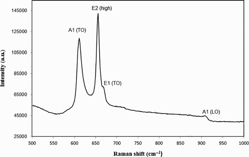
Raman spectrum of catalyst free grown AlN nanowire films: sharp and strong E2 (high) peak indicates very good crystal quality of AlN nanowires
Conclusions
The synthesis of both catalyst free and catalyst assisted growth of AlN nanowires by CVD using Al and NH3 as source materials has successfully been demonstrated. Both catalyst free and catalyst assisted growth runs have mostly been carried out at 1100°C under H2 as carrier gas. While the catalyst free growth runs resulted in long (∼40 μm) and dense AlN nanowire array films, the catalyst assisted growth resulted in short nanowires (3–5 μm). The catalyst free growth takes place through a VLS mechanism with Al droplets serving as the self-catalyzing agents, whereas the catalyst assisted growth takes place through a VLS mechanism with foreign metal catalysts serving as the catalyzing agents. Raman spectroscopy of the catalyst free grown nanowires has revealed very symmetric and strong phonon modes, which agree well with the high quality single crystalline bulk AlN. In fact, the symmetric and strong E2 (high) peak indicates very good crystal quality of the grown AlN nanowires. As a result, the catalyst free grown AlN nanowire array films provide great opportunities of their easy transfer into any substrate for the development of new devices in nanoelectronics and nanophotonics.
Footnotes
Acknowledgements
The author gratefully thanks the US Appalachian Regional Commission (ARC) for providing support for the present research. The present work was also supported by a Marie Curie FP7 Integration Grant within the 7th European Union Framework Programme. The author acknowledges the support of West Virginia University Shared Research Facilities.