
Abstract
ZnO nanowire array films, composed of well aligned ZnO nanowires ∼200 nm in diameter and 1 μm in length, were successfully synthesised on Mg doped gallium nitride by hydrothermal method. In addition, the films possess quite flatten surface. In the synthesised process, there was no catalyst that had been used. Growth conditions were comprehensively discussed in the process of aqueous solution method. It was found that the length of ZnO nanowires and the thickness of the film could be tunable by altering solution concentration and growth time. Such ZnO film assembled with vertically aligned nanowire may have potential applications as UV light emitting diodes.
Introduction
In the past decades, many kinds of nanostructures have been synthesised, such as carbon nanotubes, 1 gallium nitride (GaN) 2 and oxide metal nanowires (NWs). 3 Among them, ZnO NWs have attracted much interest due to their good performance. ZnO has a band gap as wide as 3·37 eV, and its exciton bonding energy is 60 meV at room temperature. In the same time, it also has excellent thermal stability and visible light transparency. These characteristics make ZnO NWs to have great potential applications in field emission devices, 4 nano-optoelectronics, 5 photodetector 6 and light emitting diodes (LEDs).7 8 –9 ZnO film also plays a very important role in optoelectronic devices. 10 As a kind of material with quite good transparency and conductivity, it can be applied to epitaxial electrodes on LEDs with the expectation to replace the metal electrodes, which cost much and have a relatively poor performance. ZnO film 11 and NW 12 can also be used in gas sensor and other fields. Reading et al. deposited ZnO film on GaN based LEDs, finding that white LEDs with ZnO sheet have higher luminous efficacy than devices with indium tin oxide film. 13 Kim et al. successfully grew heteroepitaxial ZnO films in water at 90°C using a two-step method, and they also demonstrated that the aqueous solution can synthesise ZnO nanowire array film (NAF) in the same growth system by changing its potential of hydrogen (PH). 14 However, how to gain large area and high quality ZnO NAF by a small amount of cost is still a hot spot in current research. As is known to us, no doping ZnO belongs to n type semiconductor material, and when ZnO NWs are synthesised on Mg doped GaN (P-GaN), the structure of ZnO NWs/P-GaN can directly formed heterojunction. It will form a heterostructural LED array,15 16 –17 which exhibits better electroluminescence performance than does ZnO film LEDs because the carrier injection efficiency can be enhanced and structural defects are decreased in these micro/nanostructures.18 19 20 21 22 –23 Meanwhile, ZnO film can make ohmic contact with P-GaN. Many people have synthesised ZnO NWs or film using different methods, such as metal organic chemical vapour deposition (MOCVD),24,25 magnetron sputtering26,27 and pulse laser deposition. 28 In the present paper, we successfully realised the synthesis of ZnO NAF on P-GaN just by changing solution concentration and growth time in hydrothermal method.
Experimental
A schematic of ZnO NAF and the substrate structure is shown in Fig. 1. Aluminium nitride (AlN), GaN and P-GaN were deposited on c-sapphire successively by MOCVD. Because of the small lattice mismatch between P-GaN and ZnO, 29 high quality ZnO nanostructures can be easily acquired on P-GaN. First, AlN sheet contained two layers: one deposited at low temperature (670°C) and another at high temperature (1100°C). Then, GaN and P-GaN were deposited at 900°C. P-GaN was annealed for 40 min at 750°C in ammonia gas atmosphere at the end. After deposition of P-GaN/GaN/AlN on c-sapphire, this template was then cleaned with alcohol, acetone and deionised water (resistivity of 18·2 MΩ cm), and placed in Teflon reaction kettle for synthesis of ZnO NAF. The solution for the ZnO growth contained zinc nitrate hexahydrate [Zn(NO3)2.6H2O] and hexamethylenetetramine (HMTA, C6H12N4). Alkaline environment was created by adding ammonia water into the starting solution. Temperature was held at 95°C in whole aqueous solution deposition process for ∼2 h, and samples were cleaned with deionised water and dried after taking them from the kettle. For the structure of P-GaN/GaN/AlN/c-sapphire, we carried out atomic force microscopy (AFM) to characterise its morphology features. Field emission scanning electron microscopy (SEM) was used to measure the surface of deposition products, and X-ray diffraction (XRD) was used to measure the quality of the NAF. Room temperature photoluminescence (PL) was employed to test the luminescence peaks of P-GaN and ZnO nanostructures using a He–Cd laser whose wavelength is 325 nm.
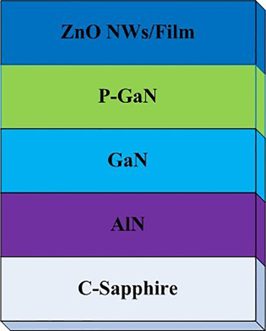
Schematic illustration of ZnO NWs/film and substrate
Results and discussion
Figure 2 shows the AFM image of P-GaN/GaN/AlN/c-sapphire structure deposited in MOCVD. As root mean square surface roughness is as small as 0·411 nm, we obtained a good template with a quite flat surface to synthesise ZnO NAF. The thickness of the P-GaN/GaN/AlN structure is ∼947 nm.
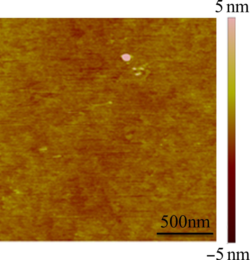
AFM image of P-GaN/GaN/AlN/c-sapphire deposited by MOCVD
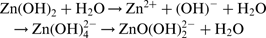
Figure 3 shows the SEM images of ZnO NAF synthesised in different experimental conditions described in Table 1. The solution pH of all the samples was set at 7·5 in the starting solution. The temperature of all the samples is 95°C. Figure 3a shows the surface morphology of ZnO NAF manufactured in 0·05 mol L− 1 solution for 2 h. The well aligned NWs with well distributed hexagonal prisms grow along the c axis and are perpendicular to the substrate. The average NW diameter is ∼200 nm and 845 nm long. When increasing the growth time to 5 h, the sample was obtained as shown in Fig. 3b. It is obvious that the density of ZnO NWs increased. The ZnO NWs are discontinuous, they have not fully coalesced, and the surface of the film shows very rough morphology. Figure 3c shows that ZnO NAF grew in 0·1 mol L− 1 concentration for 5 h. In this condition, the ZnO NAF uniformly covered the entire template surface. The thickness of the film is 1·95 μm, much bigger than those of the previous ZnO NAFs. Figure 3d shows ZnO film synthesised in 0·1 mol L− 1 concentrations for 7 h, and we obtained a very dense film without any aperture that appeared in Fig. 3c. The right side of SEM image is the cross-sectional picture of each corresponding sample. Among these samples, ZnO NWs have been synthesised with very high density that it was hard to distinguish in the corresponding cross-sectional picture. Furthermore, we find that the thickness of ZnO NAFs is altering with solution concentration and growth time. When using growth time of 5 h and solution concentration of 0·1 mol L− 1, the thickness of ZnO NAF grew 1·952 μm. The chemical reaction equations of generating ZnO can be described as follows:

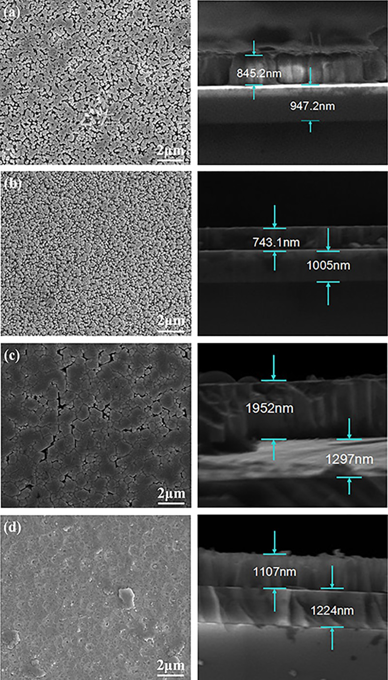
SEM images of ZnO NWs and film synthesised in different experimental conditions: a 0.05mol/L,2h, b 0.05mol/L,5h, c 0.1mol/L,5h, d 0.1mol/L,7h; left – vertical top view from sample surface and right – cross-sectional view
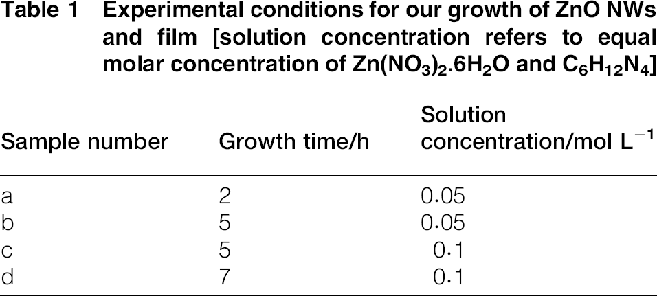
Experimental conditions for our growth of ZnO NWs and film [solution concentration refers to equal molar concentration of Zn(NO3)2.6H2O and C6H12N4]
The crystal structure is characterised by XRD measurement. Figure 4 shows the XRD patterns of ZnO NAFs. Before depositing ZnO NAF on P-GaN, the P-GaN XRD was also carried out to characterise its crystal structure to compare with ZnO diffraction patterns. There is a very strong peak at 2θ = 34·4°, obtained from ZnO (002) crystal plane, consistent with the accepted diffraction angle, as labelled on the XRD image. So the strong peak observed signifies that our ZnO NAFs grew along the c axis, revealing preferential orientation in the [002] direction, and this result agrees well with the SEM images that present a very good orientation along the c axis. Such growth behaviour has been clarified by the chemical bonding theory of single crystal growth,31 32 –33 that is, the crystallographic structure thermodynamically determines the growth habit of condensed matters. The peak of P-GaN is located at 2θ = 34·6°. The peak of samples a, b and d split into two peaks: the left ones are obtained from ZnO, and the right ones are contributed by P-GaN (002). These two peaks are so close that they are very difficult to distinguish. In addition, the XRD pattern of sample c did not find the peak of P-GaN due to the large thickness of ZnO layer, which entirely covers the whole P-GaN surface as demonstrated in the SEM images. At the same time, sample d exhibits a smaller peak than do samples a, b and c. For sample d, the ZnO film is composed of ZnO NWs. With growth time increasing, these NWs have fully coalesced to produce a rough surface morphology. There may be some lattice mismatch dislocations in the coalesce interface between NW and NW; this will lead to crystal quality of sample d worse than those of samples a, b and c.
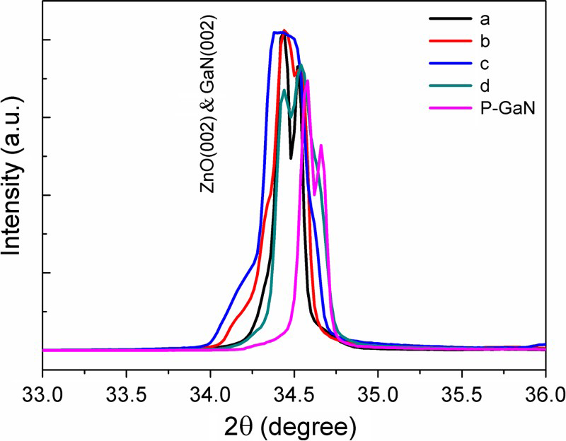
XRD patterns of ZnO NWs (a, b) and film (c, d) on P-GaN, and P-GaN diffraction pattern was shown for comparison in picture
PL measurement was performed on the n-ZnO/P-GaN heterojunction since it was an effective method for investigating the presence of defects. In addition, all the PL spectra were measured at room temperature, as shown in Fig. 5. The PL spectrum of P-GaN template was obtained before it was used to grow ZnO. The near band edge emission peak observed in the PL spectrum for the GaN at ∼360 nm is rarely observed in the ZnO films, indicating that the surfaces of P-GaN were covered entirely by NWs. A strong UV emission centred at 379 nm and a weak and broad green emission centred at 575 nm of all the n–p heterojunction were observed. The UV emission is usually considered as the characteristic emission of ZnO, and the UV emission peak usually originates from the near band edge emission from the recombination of free excitons. 34 Generally speaking, the green emission centred at 518 nm is attributed to the singly ionised oxygen vacancy in ZnO, and the emission results from the radiative recombination of a photon generated hole with an electron occupying the oxygen vacancy.35,36 However, Zeng et al. deliberated that the violet and blue emissions are attributed to the transitions from Zni and extended Zni states to the valance band respectively. 37 According to Zeng et al.'s report, the UV emission complies with their excitation modes. For the violet emission, if the electrons are excited up to a sub-band of the conduction band, they can first relax to Zni state through a non-radiative transition and then transit to the valance band. So the excitation mode is effective for violet emissions. From the PL spectra, UV intensity of sample A is much stronger than those of other samples, implying that it is easier to make the electrons to Zni state through a non-radiative transition. In contrast, green emission is usually efficient with the transition from the conduction band to deep levels. 37 For sample A, the transition from the conduction band to deep levels is existent. So the coexistence of several types of defects may be the result of higher intensity in sample A than in others in 518 nm, the radioactive recombination wavelength. 37 For the ZnO NAFs grown on the P-GaN film, it often acts as a spreading layer deposited on the materials of active region in LEDs.
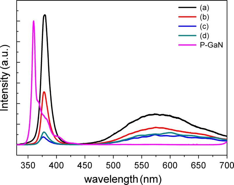
PL spectrum of ZnO NWs and film at room temperature; PL spectrum of P-GaN template was also displayed for comparison; all of these ZnO samples did not experience annealing procedure
Conclusions
In summary, we finished the synthesis of ZnO NAF on P-GaN with no use of catalyst in the same aqueous solution growth system simply by changing solution concentration and growth time. Cross-section SEM images show that the thickness of ZnO NAFs is changing with solution concentration and growth time. XRD and PL results show that the ZnO NAFs have high quality crystals. The strong diffraction peak of ZnO (002) crystal plane at 2θ = 34·4° was observed in the XRD pattern, revealing that we obtained single crystals that grow along the c axis of the crystal plane and have a good orientation in [002] direction. UV intensity of sample A, possessing sparse NW array, is much stronger than those of other samples. Taking use of this feature, many researchers have utilised ZnO NW array to make heterojunction with P type materials, since ZnO is a kind of native N type material.
Footnotes
Acknowledgements
This work is supported by the National Natural Science Foundation of China (grant no. 61405076), the Hubei Province Science Fund (grant nos. 2008CDB334 and 2011CDB049), the Starting Research Fund from the Jianghan University (grant no. 2012017) and the Open Project of State Key Laboratory of Functional Materials for Informatics.