
Abstract
Diamond film was grown on high thermal conductivity graphite substrate using microwave plasma chemical vapour deposition method. Nanodiamond particles were uniformly seeded on the substrate to generate high nucleation density by a spray gun. The continuous and high purity diamond film was obtained, and growth rate was up to 2.7 μm h− 1. The thickness, surface morphology, quality and composite phase of the film were analysed by SEM, Raman and X-ray diffraction. It was shown that graphite coated with diamond presented a higher thermal conductivity (520 W m− 1 k− 1) than copper. Furthermore, this coated material with high thermal conductivity, good strength and non-conductive surface will make it possible to be widely used in thermal management field.
Introduction
Thermal conductivity in electronic package design is becoming increasingly important for the high power electronic devices that generate more and more heat, such as high power laser diodes, laser heat conductors, megawatt power gyrotrons and UV LEDs. 1 Chemical vapour deposition (CVD) diamond was investigated for the next generation thermal management materials as its potential properties,2,3 which includes high thermal conductivity (TC) and low coefficient of thermal expansion. 4 However, the production time of 1 mm thick diamond sheet is so long, and the price is of which so high.
In order to lower the price of diamond, the diamond film grown on the high TC graphite (HTCG) with low coefficient of thermal expansion matching with diamond can be used as thermal conductor. The combination of diamond and graphite overcomes the defect that graphite powder is easy to fall off from the surface of graphite block.5,6 In the present paper, the polycrystalline diamond films coated with graphite substrates were investigated for obtaining high TC material with non-conductive surface, which would be applied in a traditional thermal management system.
In the diamond deposition process, non-diamond substrates need to be treated before the growth of diamond to enhance the nucleation density, which is called diamond seeding pretreatment. Such commonly used pretreatment techniques include abrading,7,8 ultrasonic nucleation,9,10 bias enhanced nucleation,11,12 and interlayers. 13 In the present study, in order to generate a high seeding density, seeding particles were covered on the substrate using a spray gun. After depositing diamond film on the graphite substrate, high TC, non-conductivity coating material will make it possible to step into thermal industries application.
Experimental
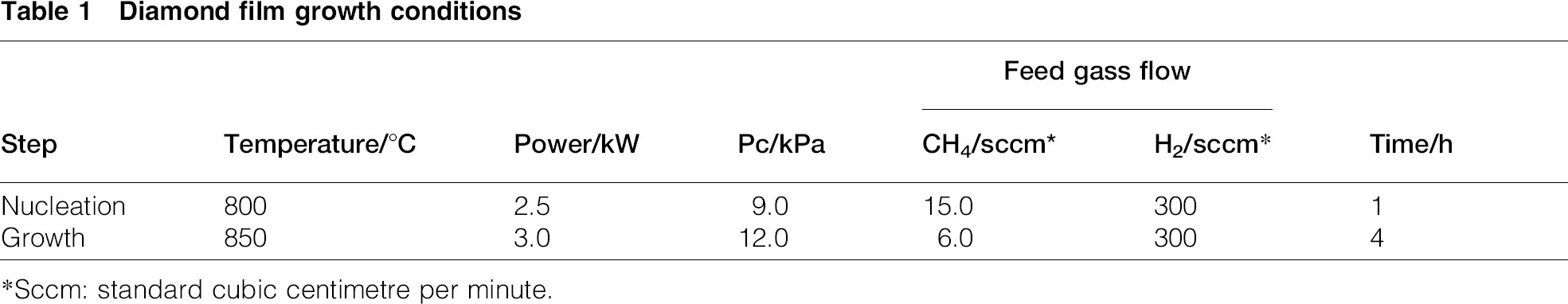
Polycrystalline diamond films were grown on the HTCG (supplied by Institute of Coal Chemistry, Chinese Academy of Sciences) by microwave plasma CVD system (2.45 GHz, 5 kW, water cooled stainless chamber). The HTCG substrate was uniformly seeded with diamond powders (size of 15 nm) using an airbrush shown in Fig. 1, and the traditional method by scratching was also worked as a comparison. The main deposition parameters were listed in Table 1. After evacuation of the chamber (2 × 10− 2 Pa), H2 (purity level 99.999) gas was introduced and after 10 min, and CH4 (purity level 99.999) flow was started. The pressure was ∼9.0 kPa during the diamond nucleation process, and after 1 h, it will be maintained at 12.0 kPa in the deposition process. The gas flow rates were controlled by mass flow controllers, and the substrate temperature was ∼850°C measured with a two-colour infrared radiation thermometer.
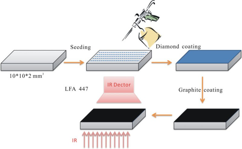
Schematic fabrication process steps of diamond film growth on graphite substrate (diamond powders were covered on cleaned substrate with airbrush, then diamond films were coated after nucleation and growth, and finally, thermal diffusivity was tested)
Diamond film growth conditions
*Sccm: standard cubic centimetre per minute.
The morphology of the substrate, the quality of diamond and the composited phase of film were analysed by field emission scanning electron microscope (FEI QUANTA 250 FEG, HITACHI S-4800), Raman spectroscopy (Renishaw spectrometer, 532 nm He–Ne Red laser), X-ray diffraction (XRD; Philips PW3710, Cu Kα) and thermal diffusivity α (NETZSCH Laser Flash Apparatus 447).
The substrates were cleaned using acetone methanol and deionised water for 5 min respectively. Then, the substrates were put into the chamber following with subsequent nucleation and growth. Finally, the thermal diffusivity of graphite substrates was tested after deposition of diamond film at room temperature. The thermal diffusivity α of the materials was tested with the process as shown in Fig. 1, and then the TC was calculated based on the diffusivity using the follow equation
14

Result and discussion
The SEM image of the diamond film with 5 h deposition is shown in Fig. 2, and different nucleation methods were used in the experiment. The results of spray seeding and traditional scratching seeding methods are presented in Fig. 2a and b. Under the same growth condition, scratching seeding nucleation method showed the discontinuous film in Fig. 2b, and the round grains were isolated covered on the graphite substrate. At the top of the grain surface, the (100) planes were showed, and the size is much smaller than the novel nucleation method. Figure 2a shows that continuous and uniform diamond films were grown on the graphite surface, a very intense (100) planes were observed on the surface of the diamond films, and a little amount of other planes such as (111) and (110) were also recorded in the image. High magnification SEM is presented in Fig. 2c that the crystal orientation was in disorder and there were a large amount of twins and crystal boundaries. Some of the grains were as large as ∼15 μm, which can be attributed to the effect of the crystal competitive growth. 15 Fig. 2d indicated that the polycrystalline diamond film showed a columnar structure, and its thickness was ∼13.5 μm; thus, the growth rate of the film was calculated to be 2.7 μm h− 1. It was worth noting that the continuous film shows a high nucleation density as the novel seeding method using a spray gun, which guaranteed that the HTCG substrate was uniformly covered by diamond particles. Compared with traditional pretreatment method such as scratching in the present paper, the novel method was much more effective and easier.
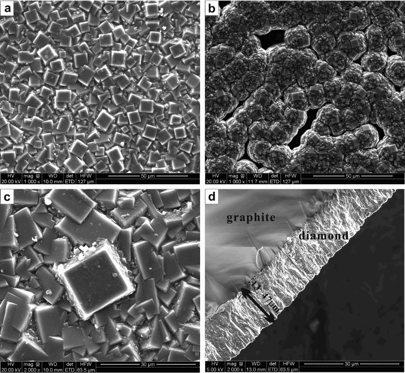
Images (SEM) of substrate surface after deposition by a spray and b scratching seeding methods; magnification of c morphology and d section was also presented
Further information on the nature of diamond film grown on the graphite block surface is provided by the Raman spectra in Fig. 3. The Raman spectra were collected with a Renishaw Raman microscope (532 nm laser excitation wavelength). Only the strong and sharp peak at 1332 cm− 1 (wave number) was found, without sign of sp2 bonded carbon, which means the high purity of diamond. The width at half maximum of the diamond peak was ∼4.6 cm− 1, indicating that the diamond film was of very high quality. 16 Traditionally, diamond is formed by an infinite extension of sp3 carbon–carbon bonds. However, since diamond is not a thermodynamically stable phase, much sp2 bonded carbon often accompanies with the CVD diamond deposition. The sensitivity of Raman spectroscopy for even very small amounts of sp2 carbon makes it the technique of choice to study these films. The sp3 bonding in Raman spectra is indicated by Peak, located at 1332 cm− 1. For microcrystalline graphite (sp2 bonding), the first order and second order peak are at 1580 and 1360 cm− 1 respectively. From the Raman spectra, the peak was located in 1332 cm− 1, which indicated none or little of compressive stress in this film and the good quality of diamond film.
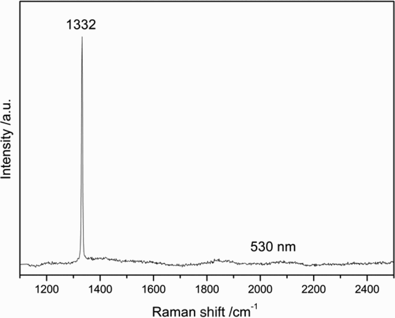
Raman spectra of diamond film deposited on graphite substrate
The grain size and crystal orientation of the diamond film were investigated by utilising XRD spectra, as shown in Fig. 4. (111), (220), (311), (400) diffraction peaks located at 2θ = 43.9, 75.3, 91.4 and 119.5° were presented in the SEM image. (111) peak became dominant after deposition. The average grain size could be calculated based on the diffraction peak using the well known Sherrer's equation
17
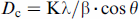
X-ray diffraction spectra reveals growth of diamond film on graphite substrate
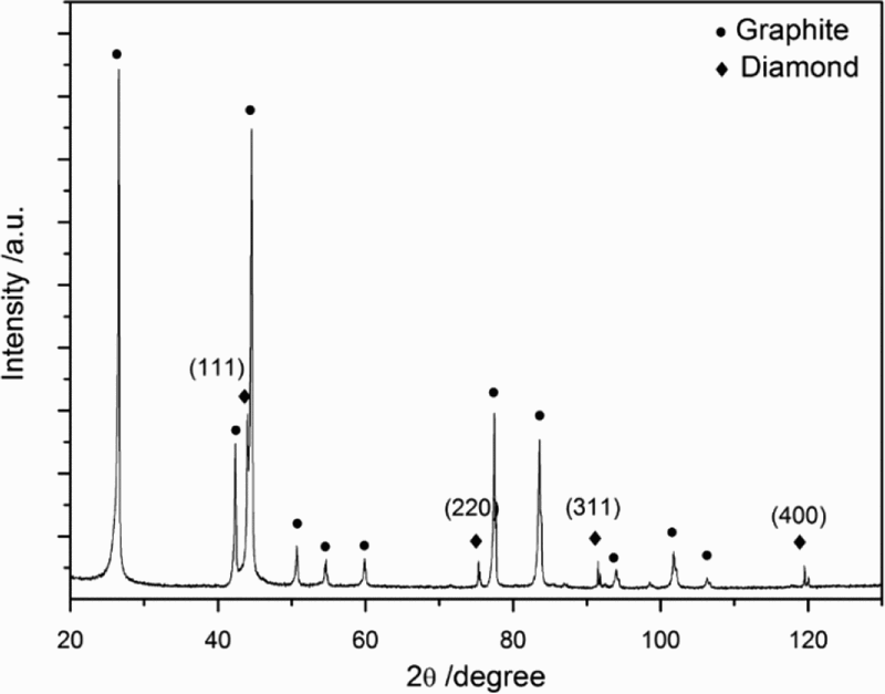
Figure 5 shows the thermal conductivities of the graphite substrate, diamond coated graphite, copper and aluminium at room temperature. The thermal diffusivities of raw graphite sample and graphite substrate coated with diamond film were 220 and 280 m2 s− 1 respectively at room temperature. It could be seen that the TC of graphite substrate rose up to 520 W m− 1 k− 1 after deposition process of diamond film, comparing with 420 W m− 1 k− 1 before diamond deposition. During the diamond film deposition, the carbon atoms would be bonded with the graphite substrate and reacted with radicals, gas molecules, ions, etc. from the plasma ball. 19 Therefore, the carbon atoms would fill up the gaps of the graphite substrate, which was the reason that the TC was enhanced. Comparing with other general thermal materials, such as copper (397 W m− 1 k− 1) and aluminium (240 W m− 1 k− 1), the diamond film coated on graphite substrate would be more excellent for use as thermal conductive products. In addition, low density was demanded for an electronic product. This graphite with diamond film (2.1 g cm− 3, close to the graphite substrate) also showed a lowest density compared with copper (7.8 g cm− 3) and aluminium (2.7 g cm− 3). Furthermore, the resistance of the graphite was also changed significantly after electrical performance test. The surface resistance increased from 0.5 to 2500 Ω after deposited diamond film on the graphite. It is worth pointing out that the material that becomes the insulator would be more suitable for used in semiconductor.
Thermal conductivity of diamond coated on graphite substrate
Although graphite featured high TC, it was difficult to be used as the electronic product because graphite particles easily to falls off from the body, which would reduce the stability of the product. Therefore, coating diamond on the graphite would effectively solve this problem. In Fig. 6, the surface scratching tests of graphite substrate before and after diamond deposition indicated that the surface strength was improved after diamond deposition. The parameters of scratching test were as follows: begin load 1 N, loading rate 15 N min− 1, end load 10 N, length 3 mm and diamond indenter radius 200 μm. As shown in Fig. 6a, the graphite was relatively soft and was broken when the load was1.0 N at the start stage of the test. However, the surface of diamond films deposited on the graphite substrate began to break at 5 N. It was obvious that diamond coatings on graphite substrate had a better strength, which was enough to be used in heat spreader area. Figure 7 revealed the structure of the diamond coatings on graphite substrate applied for LED thermal conduction. In conclusion, the TC of diamond film improved a lot compared with other used materials. Furthermore, the diamond films were easy to grow on any shape of substrate, which could be widely used in thermal application.
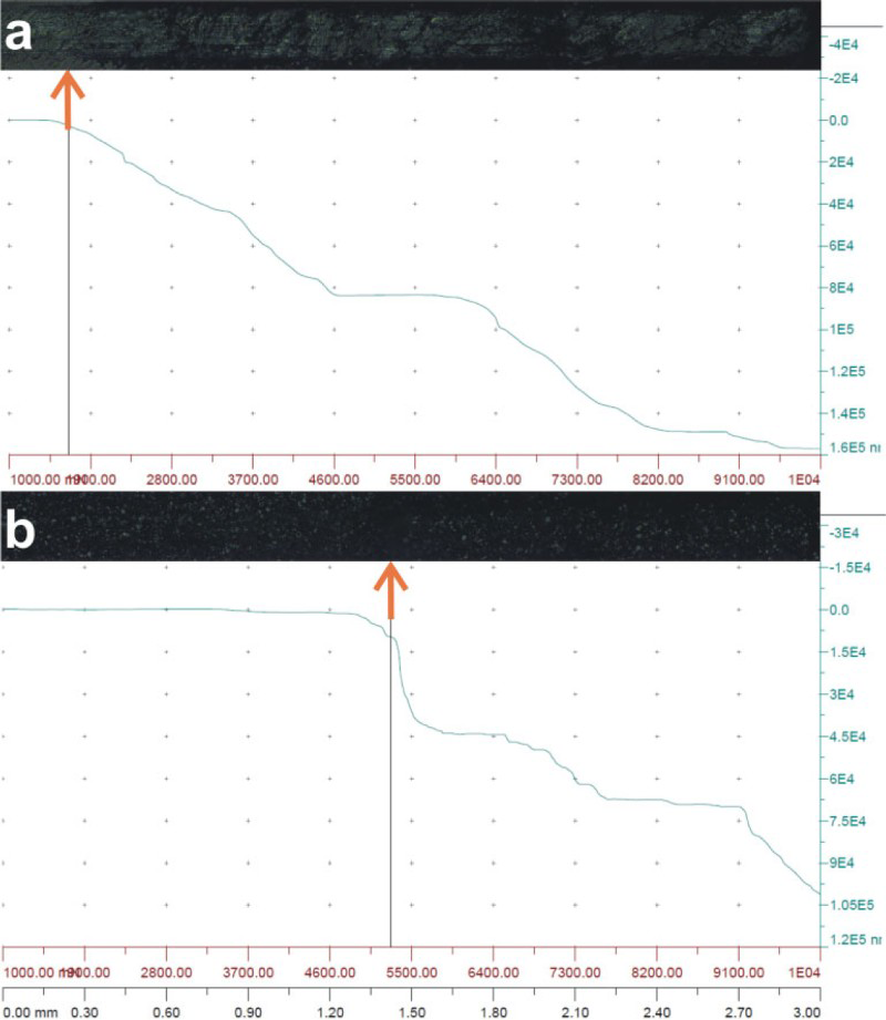
Surface scratch test a before and b after diamond deposition
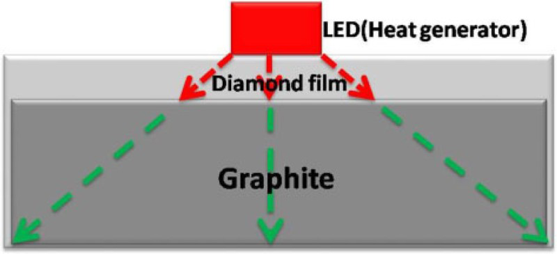
Structure of led thermal materials by diamond coated graphite
Conclusions
In the present study, polycrystalline diamond film with uniform nucleation has been deposited on HTCG substrate. Using a new method of seeding pretreatment, good continuity and quality diamond film were formed according to characterisations of the SEM, Raman XRD spectra. The thermal diffusivity increased from 220 to 280 m2 s− 1, and TC rose up from 420 to 520 W m− 1 k− 1 after diamond film deposition. Furthermore, it had a higher strength than graphite and was not easy to fall off as graphite. In summary, it is of high potential to be widely used in thermal management field.