
Abstract
Ultrathin films of TiO2 were grown on a W(100)–O(2 × 1) substrate and characterised with a combination of scanning tunneling microscopy (STM) and low energy electron diffraction. In addition to islands of rutile TiO2(110) with (1 × 1) termination that were reported previously, we also observed rutile TiO2(110) islands with a (1 × 2) film termination. A lepidocrocite-like TiO2 nanosheet was also observed on the W(100) surface. High resolution STM images show that the nanosheet grows in the principal orthogonal directions of the W(100) substrate and forms a commensurate (1 × 7) coincident cell.
Introduction
There is great interest in the study of oxide surfaces. 1 This is due to their use in a multitude of applications, including catalysis and electronics.2–5 In many of these studies, thin oxide films are used.2,6 Thin film alternatives to bulk oxides supported on conducting substrates are typically employed to make insulating oxides sufficiently conductive to allow charged particle techniques, such as scanning tunneling microscopy (STM), to be used on otherwise insulating oxides.7,8 In some cases, such as for anatase TiO2, high quality crystals are difficult to grow and ultrathin and thin films provide an alternative to natural crystals.9–12 Structures with no bulk counterparts are of great interest as new material properties may be discovered and exploited.3,4
As the most thermodynamically stable face of rutile TiO2, the (110) face has been studied extensively.
13
Ultrathin rutile TiO2(110) islands have been grown on various substrates and are usually terminated by the (0.30 nm × 0.65 nm) (1 × 1) surface,8,14–23 but if the deposited Ti is not completely oxidised, the reduced (0.30 nm × 1.30 nm) (1 × 2) reconstruction can also be observed, where the unit cell mesh is doubled in the  direction.
16
As mentioned above, ultrathin films of anatase TiO2 have also been grown. The (001) surface generally displays a (1 × 4) reconstruction,9–12 consistent with measurements of the single crystal.24,25
direction.
16
As mentioned above, ultrathin films of anatase TiO2 have also been grown. The (001) surface generally displays a (1 × 4) reconstruction,9–12 consistent with measurements of the single crystal.24,25
TiO x films have also been reported that have no bulk counterpart, such as a quasi-hexagonal TiO x phase on Ni94Ti6(110) 26 or Ni(110)15,23 and TiO x nanodots on Ni(110). 23 A series of TiO x phases have also been grown on Pt(111),27,28 several of which are related to encapsulation layers observed on TiO2(110) supported nanoparticles.29,30 Of particular relevance to this paper are the family of lepidocrocite-like films that have been observed on Pt(110)–(1 × 2), Ni(110), Ag(100) and Pt3Ti(111).15,17,18,27,31,32 This film is so named due to its structural similarity to the FeO(OH) lepidocrocite bilayer. 33 In calculations, the lepidocrocite-like structure forms spontaneously from a (001) anatase bilayer,18,31,34,35 the top layer displacing by half a unit cell. The substrate free bilayer has lattice parameters of ∼0.375 nm × 0.300 nm.15,17,18,27,31,36
Here, we have studied ultrathin TiO2 films grown on W(100)–O(2 × 1) surfaces using STM and low energy electron diffraction (LEED). The W(100)–O(2 × 1) reconstruction is formed by removing (or adding) alternate rows of W along [001] or [010] to create {110} microfacets that contain O in the three-fold hollow sites. 37 This gives a primitive surface unit cell of 0.63 nm × 0.32 nm that is nearly lattice matched with rutile TiO2(110). Apart from the (1 × 1) phase that was previously observed, 19 we observed a TiO2 lepidocrocite-like structure as well as the TiO2(110)–(1 × 2) reconstruction for the first time on W(100).
Experimental
The experiments were conducted in an ultrahigh vacuum (UHV) system comprising a preparation and analysis chamber with base pressures in the 10− 10 mbar range, equipped with quadrupole mass spectrometers for residual gas analysis (RGA). The analysis chamber housed an Omicron UHV AFM/STM, calibrated with a TiO2 (110) single crystal, and rear view LEED optics that were also employed for retarding field Auger electron spectroscopy (AES). The films were grown in the preparation chamber, which was equipped with an ion sputter gun, an electron bombardment sample heater and metal evaporators. Before the growth of the films, the W(100) sample (Surface Preparation Laboratory) was prepared by cycles of argon sputtering and annealing to ∼1173 K in 2 × 10− 8 mbar O2 and UHV, followed by flashing to 1500–1600 K, until a well ordered W(100)–O(2 × 1) was identified in LEED and STM and any contamination was below the detection limit of AES. 19
STM images were recorded at room temperature using positive sample bias (tunneling into empty sample electronic states) and either etched tungsten or mechanically formed PtIr tips. Estimates of coverage are given in monolayer equivalents (MLE), where 1 MLE is defined as complete coverage of the surface by a single layer of TiO2 that has a thickness of 0.325 nm. Likewise, for the TiO2 lepidocrocite-like phase, 1 MLE is defined as the complete coverage of the surface by a bilayer, the thickness being estimated at 0.5 nm.
The first step of the film preparation was the deposition of 2–3 monolayers (ML) of Ti (determined retrospectively from the film coverages) onto the W(100)–O(2 × 1) surface at room temperature from the vapour of a metal wire (Goodfellow) using a commercial evaporator (Omicron EFM) with a deposition rate of 10− 2 ML− 1. The second step consisted of annealing under 2–7 × 10− 7 mbar O2 at 800–850 K between 1 and 1.5 h, followed by cooling to room temperature in UHV. The final step was a UHV anneal to 920–980 K for 10 min. Sample temperatures were measured with an optical pyrometer (Minolta). Three TiO2 films were studied, each grown under slightly different conditions: (i) a TiO2(110)–(1 × 1) ultrathin film was formed by annealing to 840 K under 2–7 × 10− 7 mbar O2 for 1 h and annealing in UHV at 970–990 K; (ii) a TiO2(110)–(1 × 2) ultrathin film was formed by annealing in 2–7 × 10− 7 mbar O2 for 1.5 h at 840 K and annealing to 920 K in UHV; and (iii) a TiO2(110)–(1 × 1)/lepidocrocite–TiO2 ultrathin film was annealed at 840 K at 2–7 × 10− 7 mbar O2 for 1 h and then annealed at 920 K in UHV.
Results and discussion
TiO2(110)–(1×1) ultrathin film
STM images are displayed in Fig. 1. In the large area (100 × 85 nm2) image of Fig. 1a, islands with mean heights of 2 nm, lengths of 15–20 nm and widths of 7–10 nm can be seen, the coverage being ∼2.4 MLE. The heights corresponds to six TiO2(110) layers, and the islands are elongated in the principal directions of the W(100) substrate. In the high resolution STM image (Fig. 1b) taken from the top of one of the TiO2(110) islands, the characteristic TiO2(110) topography can be observed. Point defects resolved between bright rows of Ti atoms are consistent with the observations of Pang et al. 19 Given that the film was left in a UHV chamber with a background water pressure of 2 × 10− 11 mbar (estimated from RGA) for 76 h after forming the film (∼3 Langmuirs), we assume that the defects are bridging hydroxyl (OHb), the coverage being 0.19 ML, where 1 ML is the density of Ti5c sites. 13
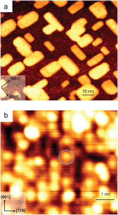
STM images (+1.6 V, 0.05 nA) of TiO2(110)–(1 × 1)/W(100)–O(2 × 1) film: a large area (100 nm × 85 nm) image, showing rutile TiO2(110) island morphology with coverage of 2.4 MLE; azimuths are defined with respect to W(100) surface; b high resolution (6.2 nm × 5.5 nm) image of surface of rutile island, six layers thick; image is characteristic of native TiO2(110)–(1 × 1) surface: bright rows are Ti atoms, with point defects between on bridging oxygen rows; blue circle highlights bridging hydroxyl (OHb); azimuths are defined with respect to rutile TiO2(110) surface
TiO2(110)–(1×2) ultrathin film
The second film was prepared in a similar manner to the (1 × 1) film described in the previous paragraph, except the final UHV anneal was at a reduced temperature of 920 K (as compared to 970–990 K). In some areas, islands of rutile TiO2(110)–(1 × 1) were observed with the same characteristics as in Fig. 1. In other regions, the islands have a different structure. Figure 2a depicts a large area image of the film. As with the (1 × 1) islands, these are also elongated in the [001] and [010] directions of W(100). Within the islands, rows can be observed and these run parallel to the direction of elongation. This row structure is more apparent in the high resolution image in Fig. 2b, and it is apparent that the rows have a spacing of 1.25 ± 0.05 nm, which is consistent with the rutile TiO2(110)–(1 × 2) reconstruction.38–51 The coverage of the film is 3.1 MLE. In Fig. 2b, the surface shown contains three different layers, all displaying the (1 × 2) reconstruction. The line profile in Fig. 2c shows that the height of the step (0.30 ± 0.02 nm) is consistent with a step edge of TiO2(110). This is the first time, to our knowledge, that the (1 × 2) surface reconstruction has been observed on an ultrathin TiO2 film on W(100). The (1 × 2) reconstruction is a reduced phase of TiO2 and is thought to be composed of added rows of Ti2O3.45,47

STM images (+1.6 V, 0.05 nA) of TiO2(110)–(1 × 2)/W(100)–O(2 × 1) film: a large area (100 nm × 100 nm) image of 3.1 MLE titania film, displaying TiO2(110)–(1 × 2) surface reconstructed islands; azimuths are defined with respect to W(100) surface; b 9.5 nm × 9.5 nm image zoomed in from light blue square in displaying (1 × 2) reconstruction; azimuths are defined with respect to rutile TiO2(110) surface; c line profiles taken from image in b; black profile displays step edge on island (0.30 ± 0.02 nm) and light blue profile shows 1.25 ± 0.05 nm periodicity in
direction, as well as another 0.30 ± 0.02 nm step edge
Such a film containing a (1 × 2) reconstruction has been previously reported in connection with a Ni(110) substrate, 16 where its appearance was attributed to incomplete oxidation of the as deposited Ti. The growth conditions for the (1 × 2) film involved a longer oxidation step than for the (1 × 1) film, and a final anneal step at a lower temperature. The lower temperature of the final anneal step may lead to incomplete oxidation of the Ti.
TiO2(110)–(1×1)/lepidocrocite–TiO2 ultrathin film
Figure 3a shows a large area STM image of the film. Two distinct overlayers were observed with quite different mean heights. The taller of these overlayers corresponds to islands of rutile TiO2(110). The islands have mean heights of 2–2.5 nm. Coexisting with these islands is a pseudo-two-dimensional or ‘nanosheet’ overlayer that has a uniform height of ∼0.5 nm. This nanosheet has a similar appearance and height to the lepidocrocite-like phases reported previously.15,17,18,27,31,36 The rutile islands have an area coverage of 25 and the nanosheet 42. This corresponds to MLE coverages of 1.7 MLE and 0.42 MLE respectively.
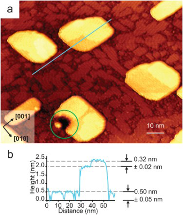
STM images (+1.6 V, 0.05 nA) of TiO2/W(100)–O(2 × 1) film: a large area 100 nm × 75 nm image of titania film; TiO2(110) islands are present together with lepidocrocite-like TiO2 nanosheet; hole in one island is circled in green and is presumably due to some interaction with tip; rutile TiO2(110) islands and lepidocrocite-like film have coverages of 1.7 MLE and 0.42 MLE respectively; b line profile taken from line indicated in a shows heights of rutile TiO2(110)–(1 × 1) island and lepidocrocite-like phase, which are 2.0–2.5 and 0.5 nm respectively
Higher resolution images of the nanosheet recorded from a different region of the sample are displayed in Fig. 4. Figure 4a is a large area image and shows a long range periodicity of ∼2.0 nm along the [010] direction of the W(100) substrate. This periodicity is more apparent in the zoomed in image of Fig 4b. The image in Fig. 4b resembles a Moiré pattern with a short lattice and a superlattice that is periodic in the W(100) [010] direction. The short lattice has dimensions of 0.37 ± 0.02 nm in the W(100) [010] direction while being exactly matched with the substrate at 0.30 ± 0.02 nm in the W(100) [001] direction. The superlattice is 2.20 ± 0.02 nm (or six times the short lattice) in the W(100) [010] direction.
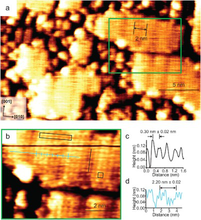
STM images (+1.6 V, 0.05 nA) of W(100)–O(2 × 1)-lepidocrocite-like film: islands of 0.5 nm height, orientated in principal directions of W(100) crystal are observed; azimuths are defined with respect to W(100) surface; a large area (25 nm × 15 nm) STM image shows islands have periodic stripes separated by ∼2 nm, with islands elongated perpendicular to these stripes; b 8 nm × 6 nm filtered image zoomed in from green rectangle in a, where primary unit cell and superlattice are visible (identified by black rectangles); minor and major ticks on blue line highlight this further; d line profile taken from black line in b displaying [001] direction unit cell spacing of lepidocrocite-like phase (0.30 ± 0.02 nm); c line profile taken from light blue line in b depicting periodicity of superlattice (2.20 ± 0.02 nm) in [010] direction
Figure 5 shows LEED patterns simulated from the real space lattice parameters together with a photograph of a LEED pattern recorded at 50 eV. Figure 5a and b depicts two orthogonal W(100)–O(2 × 1) reflexes that are calculated from the lattice parameters of W(100)–O(2 × 1). Figure 5c and d shows two orthogonal patterns with (1 × 7) periodicity with respect to W(100). These are assigned to the superlattice of the nanosheet phase. Figure 5e is a superposition of all of these, which reproduces accurately the LEED pattern presented in Fig. 5f. The {0, ½} reflexes are consistent with either TiO2(110) or W(100)–O(2 × 1). According to our interpretation of the LEED pattern, the superlattice should be seven times the W(100) lattice (0.316 nm), which gives the periodicity of the superlattice as 2.21 nm, consistent with the STM measurement.
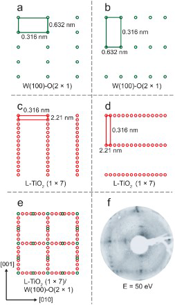
LEED patterns of TiO2 and lepidocrocite-like films on W(100)–O(2 × 1): a, b schematics of two orthogonal, calculated LEED patterns of W(100)–O(2 × 1), with real space unit cell of (0.316 nm × 0.632 nm); c, d schematics of two orthogonal, calculated LEED patterns of lepidocrocite-like film (L-TiO2) that has (1 × 7) periodicity with respect to W(100) and real space unit cell of (0.316 nm × 2.21 nm); e superposition of schematics in a–d forming predicted LEED pattern; f LEED pattern of film at 50 eV, which compares favourably with e; azimuths are defined with respect to W(100) surface
A simple model derived from the LEED and STM data is shown in Fig. 6. The substrate W(100)–(1 × 1) lattice is shown with black circles. Superimposed on this is the nanosheet layer. With respect to the azimuths of the W(100), in the [001] direction, the two are exactly matched, whereas in the [010] direction, the nanosheet layer does not coincide and has a spacing of 0.369 nm. This leads to a commensurate (1 × 7) lattice that has a period of six times the lattice parameter of the nanosheet layer and seven times the W(100) lattice.
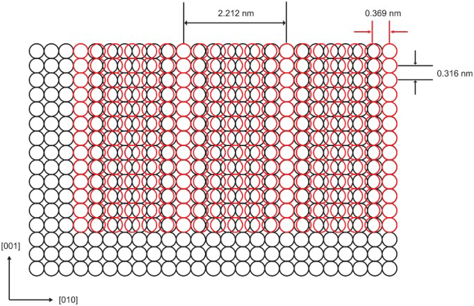
TiO2 lepidocrocite overlayer schematic: schematic representation of TiO2 lepidocrocite-like phase in red circles (0.369 nm × 0.316 nm) superimposed on top of W(100)–(1 × 1) surface (0.316 nm × 0.316 nm) in black circles; these parameters were derived from STM and LEED data; azimuths are defined with respect to W(100) surface
The theoretical lattice parameters for the substrate free TiO2 lepidocrocite-like phase are calculated at 0.373 nm × 0.302 nm by Vittadini and Casarin 34 and 0.3766 nm × 0.3007 nm by Atrei et al. 18 Thus, the long side of our nanosheet unit cell would only represent a very modest contraction of 1.1–2.1 from the calculated values of the lepidocrocite-like phase. This compares to an expansion of 3.4–4.4 to 0.39 nm for the lepidocrocite-like phase on Pt(110)–(1 × 2) 35 and a contraction of 3.2–4.2 to 0.361 nm for the same film on Ag(100).
The short side of our nanosheet unit cell (0.316 nm) also only represents a small expansion from the theoretical values of 4.3–5. For comparison, the lepidocrocite-like phase on Ag(100) has a maximum contraction of 4–4.6 to 0.289 nm, making the short direction commensurate with the substrate. The short side of lepidocrocite-like phase unit cell on Pt(110)–(1 × 2) was measured in STM to have a length of 0.30 nm. This had an identifiable × 14 super cell with respect to the substrate in the [001] azimuth (0.277 nm).
As for the height of our nanosheet film, this was measured in STM to be 0.5 ± 0.05 nm. This is in agreement with the height of the lepidocrocite-like film on Ag(100) as determined by X-ray photoelectron spectroscopy and LEED intensity measurements. 18 On the other hand, Agnoli et al. 35 report an apparent height in STM of ∼0.15 nm on Pt(110)–(1 × 2) but attribute this to electronic effects.
From this comparison, we conclude that our nanosheet phase is also a lepidocrocite-like phase. If the underlying substrate was W(100)–O(2 × 1), this would imply a × 3.5 coincident lattice in the W(100) [010] direction. As such, we believe that the oxygen from the W(100)–O(2 × 1) is incorporated into the lepidocrocite-like phase, which is then formed directly on the W(100) surface.
Poor stability of a delaminated titanate bilayer was observed previously by a transformation into anatase crystallites >1070 K, 52 and we tested this on our film by annealing the sample to 1000 K. The (1 × 7) LEED spots were considerably weakened in intensity. Likewise, whereas before annealing the lepidocrocite-like overlayer had area coverage of 42, this was reduced to 3.3 after annealing. The formation of the lepidocrocite-like phase may be related to the lower temperature of the final UHV step in comparison with the (1 × 1) film. In the two studies by Atrei et al.,17,18 for the same growth conditions, the lepidocrocite-like phase was observed for up to one ML of Ti deposition, beyond which rutile TiO2(110) islands coexist on the surface. Thus, another explanation for the appearance of the lepidocrocite-like phase in the current work could be related to the lower coverage of Ti used to make this film in comparison to the two rutile TiO2 films presented.
Conclusions
We used STM to image rutile TiO2(110)–(1 × 2) islands supported on W(100)–O(2 × 1). In addition, a TiO2 lepidocrocite-like nanosheet was also shown to grow on W(100) and was characterised by STM and LEED. The unit cell of the film was 0.369 nm × 0.316 nm. The short side of the lattice was directly coincident with the W(100) substrate in one of the principal directions. A commensurate superstructure with respect to the substrate of 2.21 nm × 0.316 nm was observed. The modulation in height observed in STM had a period of 2.21 nm, six times the unit cell of the film and seven times the unit cell of the W(100) substrate.
Footnotes
Acknowledgements
This work was supported by the European Research Council Advanced Grant ENERGYSURF (GT), SABIC, the Royal Society (UK), and Alexander von Humboldt Stiftung (Germany), COST Action CM1104 “Reducible oxide chemistry, structure and functions”, which funded MCS's visit to London.