
Abstract
III-Nitrides are materials that have revolutionised the lighting industry allowing for the development of high brightness and efficiency white light emitting diodes (LEDs), enabling cost and energy savings at an unprecedented scale. However, there remain several obstacles to the further enhancement of the efficiency of LEDs, particularly for emission at longer wavelengths. The existence of polarisation fields as an inherent property of wurtzite III-nitride materials severely hampers LED performance. The origin of these fields due to the deviation from an ideal tetrahedral bonding structure and their relation to strain has been addressed in this review. The effect of the polarisation fields on the band structure of heterostructure quantum wells, known as the quantum confined stark effect, and its implications for the efficiency and spectral stability of LEDs have also been reviewed. Finally, the effectiveness and viability of several proposed methods of mitigating the harmful effects of the polarisation fields, such as the growth of III-nitrides on alternative planes, doping, strain engineering and growth of cubic GaN, have been addressed.
This review was awarded a runner up prize in the 2015 Materials Literature Review Prize of the Institute of Materials, Minerals and Mining, run by the Editorial Board of MST. Sponsorship of the prize by TWI Ltd is gratefully acknowledged.
Introduction
Gallium nitride (GaN), indium nitride (InN), aluminium nitride (AlN) and their associated alloys are a family of materials known as ‘III-nitrides’. This particular branch of the III–V semiconductor family has radically altered the lighting industry due to the high efficiency and brightness of short wavelength III-nitride light emitting diodes (LEDs) and laser diodes. The global push towards efficient lighting has generated considerable interest for materials research in III-nitrides in the past two decades, culminating in the Nobel Prize for physics being awarded in 2014 to S. Nakamura, H. Amano and I. Akasaki for their pioneering work on GaN LEDs. 1 The true breakthrough in lighting with regard to III-nitride LEDs is their ability to emit light brightly and efficiently in the blue to UV spectral range, properties without which it would be extremely difficult to produce white light LEDs. The worldwide replacement of traditional lighting sources such as incandescent bulbs with LEDs, perhaps best highlighted by China's recent ban on traditional lighting sources, 2 is a clear demonstration of the incredible impact that III-nitrides have had on the world since the demonstration of the first high brightness blue LED. 3
Much of the research in III-nitrides since their first implementation in optoelectronic devices two decades ago 3 has been focused on mitigating material issues that adversely affect device performance. One of the principal issues is related to crystal quality and originates from the fact that most GaN films are grown on lattice mismatched substrates due to the high cost of bulk GaN substrates, 4 resulting in the presence of numerous defects that are detrimental to device performance. 5 Bennett 5 has reviewed the somewhat controversial origin of these defects and methods for reducing their density; as such, this review will not focus on this particular issue. Instead, another critical issue that is inherent to the material system will be addressed in this review: III-nitrides are commonly grown along the c direction [0001] resulting in the presence of internal polarisation fields along the growth direction that have a devastating effect on LED performance. This work will first review the origin of these polarisation fields and the precise mechanisms through which they hamper LED performance. Following the discussion of the origin and effects of polarisation fields in III-nitride optoelectronics, methods for the mitigation of these effects and their viability will also be reviewed.
Properties of III-nitrides
III-Nitrides crystallise in two types of crystal structures: hexagonal (wurtzite) and cubic (zinc blende and rock salt). Hexagonal lattice III-nitrides have been the primary subject of academic and industrial investigations as they are more structurally stable under ambient conditions, although there has also been some interest in the study of cubic III-nitrides for LED applications. 6 III-Nitrides can exist in two polarities, depending on the orientation of the initial layer deposited on the substrate during growth, due to the lack of inversion symmetry in the (0001) plane. 7
The considerable interest in III-nitrides for optoelectronic applications is primarily due to a large direct bandgap range attainable through alloying, as shown in Fig. 1.
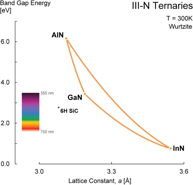
Bandgap energy against lattice parameter for III-nitrides at 300 K (Ref. 8)
The bandgaps attainable through alloying are represented by the solid lines connecting the end members. The direct bandgap of III-nitrides is a vital property in their application in photonic devices as this allows for the efficient absorption and emission of photons without the need for phonon interactions. There is considerable interest in the use of III-nitride materials for optoelectronic applications, as they can, in theory, be designed to emit and absorb light across the entire visible, infrared and ultraviolet ranges.
III-Nitrides are most commonly grown by metal–organic vapour phase epitaxy (MOVPE) 5 but are also grown using halide vapour phase epitaxy (HVPE), molecular beam epitaxy and reactive sputtering. 9 Most III-nitride films are grown on foreign substrates (heteroepitaxially) due to the high production cost of bulk GaN substrates. 4 Silicon, silicon carbide and sapphire are all used as substrates for the growth of III-nitrides, although all exhibit a lattice mismatch with III-nitrides, resulting in issues with crystal quality. 4
Polarisation fields in III-nitrides
III-Nitride materials in wurtzite form are known as polar materials, which means that they exhibit spontaneous polarisation without the presence of an external electric field.
10
The orientation of the spontaneous polarisation is along the  direction and thus can only be manipulated by changing the polarity (Ga/N polar) of the GaN. The origin of this spontaneous polarisation is the deviation from an ideal tetrahedral coordination along the (0001) axis for the III-nitride wurtzite crystal and the ionicity of the crystal (the difference in respective electronegativities of the two elements forming a bond).
11
As a result of these conditions, each unit cell exhibits a non-zero dipole moment in the
direction and thus can only be manipulated by changing the polarity (Ga/N polar) of the GaN. The origin of this spontaneous polarisation is the deviation from an ideal tetrahedral coordination along the (0001) axis for the III-nitride wurtzite crystal and the ionicity of the crystal (the difference in respective electronegativities of the two elements forming a bond).
11
As a result of these conditions, each unit cell exhibits a non-zero dipole moment in the  direction, as shown schematically in Fig. 2.
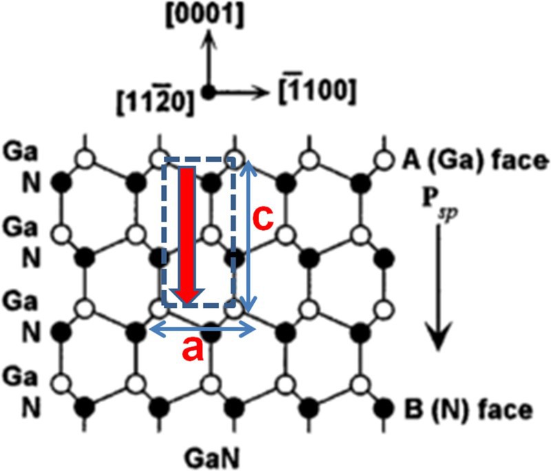
Crystal structure for GaN, with unit cell (dashed line), dipole moment (arrow) and lattice parameters a and c 12
This effect is particularly pronounced for III-nitrides compared to other III–V semiconductors as nitrogen is the most electronegative and smallest group V element, resulting in a metal–nitrogen bond with far greater ionicity than other III–V bonds. 13
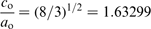
For an ideal hexagonal closed packed crystal with zero spontaneous polarisation, the ratio of the lattice parameters c0 and a0, if all nearest neighbour bond lengths are equal as denoted in Fig. 2, is given by
Bulk c/a ratios for AlN, GaN and In
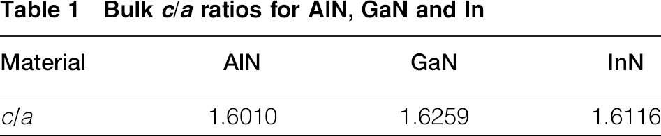
As the c/a ratio decreases, the angle between the three bonds at the base of the tetrahedral bonding structure increases, resulting in a lower compensation polarisation along the c-axis and an enhanced spontaneous polarisation. 13 As shown in Table 1, the strongest spontaneous polarisation is observed in AlN and the weakest in GaN.
Materials that exhibit spontaneous polarisation also exhibit a piezoelectric polarisation. 10 Any strain experienced by the crystal will distort the crystal lattice, in some cases further exacerbating the deviation from an ideal c/a ratio and resulting in the presence of an additional polarisation.
The piezoelectric polarisation is an important consideration when evaluating polarisation fields in III-nitrides as most films are grown heteroepitaxially and devices are typically heterostructures: in-plane lattice constant mismatches with the underlying layer result in the expansion or contraction of the III-nitride film. Biaxial compressive stress results in a decrease of the in-plane lattice parameter a and an increase in the vertical lattice parameter c, returning the c/a ratio towards its ideal value and thus resulting in a piezoelectric polarisation that opposes the spontaneous polarisation. On the other hand, if tensile stress is applied in the c direction, the c/a ratio is lowered, and the overall polarisation is increased as the spontaneous and piezoelectric components now act in the same direction. 13 This interestingly results in two different polarisation configurations for the two common ternary alloys of GaN (AlGaN and InGaN) when coherently strained to GaN. In the case of InGaN, the piezoelectric field actually acts against the spontaneous field, whereas with AlGaN the piezoelectric field acts in the same direction.
Light emitting diodes: Basics and operation
Light emitting diode structures for visible light application typically use InGaN/GaN quantum wells (QWs) for the active region. A general LED structure is shown in Fig. 3.
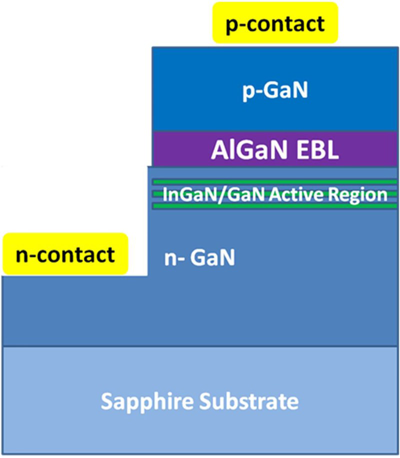
Visible light LED structure on a sapphire substrate. A forward bias applied to the structure through the metallic contacts at the p and n regions causes electrons from the n-GaN and holes from the p-GaN to flow towards the active region, these carriers then recombine to generate light. The AlGaN electron blocking layer (EBL) serves to stop electrons from entering into the p-type region
The structure typically contains a magnesium doped p type region containing free positive carriers and a silicon doped n type region containing free electrons. In order to avoid the leakage of electrons into the p-GaN region, AlGaN (a material with a higher bandgap than GaN) is used as an electron blocking layer.
The active region, composed of QWs formed by alternating InGaN and GaN layers, captures the carriers that recombine to emit photons. Carriers can also combine non-radiatively through the emission of a phonon rather than a photon. Phonons are essentially quantised lattice vibrations, or heat, and negatively affect the performance of the LED in addition to quenching light emission. Owing to their nature as charged particles, electrons and holes in the QWs can be bound by Coulombic attraction to form charge neutral quasi-particles known as excitons. These excitons can decay to emit light, albeit at an energy slightly lower than for free carriers due to their original binding energy.
Light emitting diode active regions: QWs
The first successful III-nitride LED consisted, in its entirety, of a p–n junction of a single material, known as a ‘homojunction’. 14 However, LED structure designs have since moved on and are now primarily composed of heterostructures known as QWs.
Quantum wells are composed of a thin layer of low bandgap material, typically on the order of several nanometres, in between two high bandgap quantum barriers (QBs). This results in the confinement of carriers in the low bandgap region in one direction, hence the term ‘quantum well’. This quantum confinement leads to the discretisation of carrier wave functions within the well.
Two effects arise from this confinement with regard to optoelectronic devices: the carrier recombination probabilities and thus the efficiency of the device is enhanced and the emission wavelength of the structure is blue shifted relative to the emission of the bulk material due to the introduction of bound states. 14
In a typical LED structure, the QW is positioned between the p and n doped regions of the device, allowing it to capture carriers flowing from one side to another under the application of a forward bias.
For III-nitride LEDs emitting in the blue region of the visible spectrum, GaN is typically alloyed with In at mole fractions of around 10–20 to achieve an appropriate bandgap for the QW region, with the QBs consisting of GaN. 15 While QWs are typically schematically illustrated as having abrupt interfaces, it should be noted that typical compositional profiles are not square,16–19 and hence, deviations from the potential profile illustrated in Fig. 4 occur. Equally, the challenges of growing these very thin layers may mean that in a multiple QW structure, while the intended structures have constant composition and thickness, variations throughout the QW stack may occur. 17
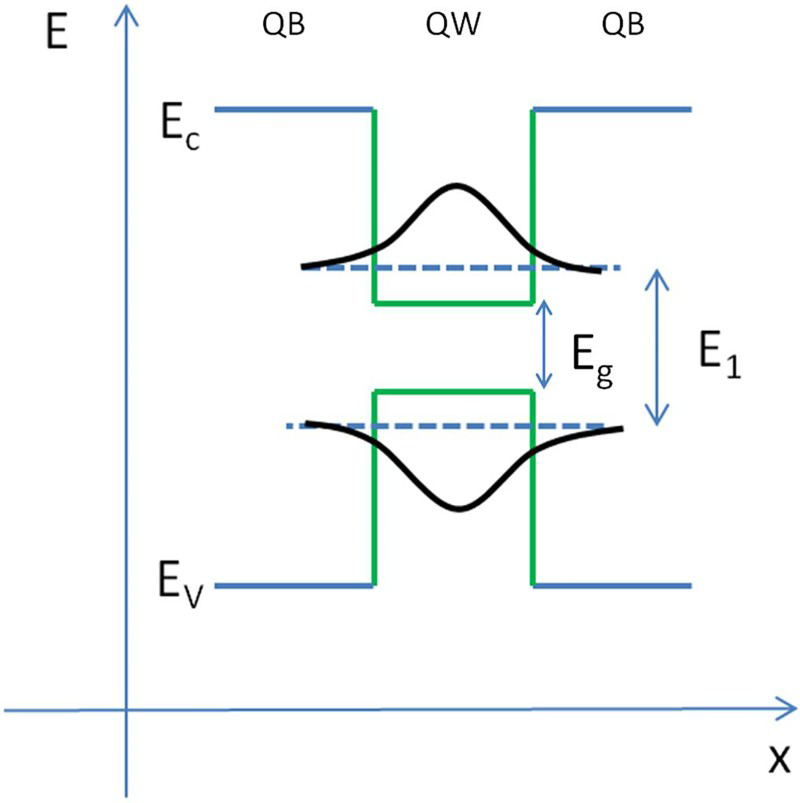
Energy-band diagram of a quantum well. The conduction and valence band edges are denoted Ec and Ev respectively. The bandgap of the well material is denoted Eg and the energy of the ground state transition is denoted E1
Quantum confined stark effect in III-nitrides
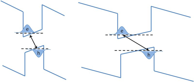
The origin of the quantum confined stark effect (QCSE) was first reported by Miller et al. for aluminium gallium arsenide (AlGaAs) QWs based on the observation that electric fields applied perpendicular to the QW layers resulted in large red shifts in absorption. 20 The mechanism behind this shift is illustrated in Fig. 5.
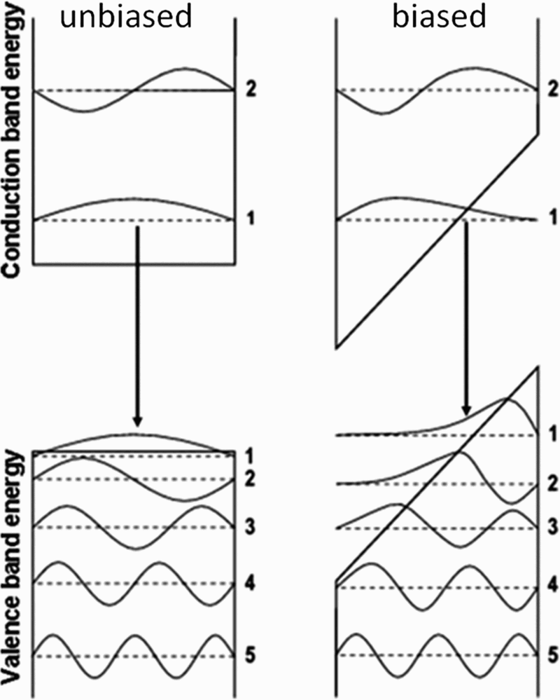
Quantum well energy levels for unbiased and biased structure with carrier wave functions for different energy levels; 21 applied bias reduces overlap between carrier wave functions
The applied potential changes the QW from a rectangular to a ‘sawtooth’ shaped well, resulting in the reduced overlap of the electron and hole wave functions as they are pushed in opposite directions.
In the context of III-nitride LEDs, it is important to consider the spontaneous and piezoelectric contributions to the overall QSCE. In the case of InGaN/GaN heterostructures for visible light LEDs, the QSCE is dominated by the piezoelectric contribution 22 to polarisation fields due to the large lattice mismatch between GaN and InN (∼11). 23 The compressive strain experienced by a 3 nm InGaN QW between two 15 nm GaN QBs and the consequent piezoelectric polarisations are illustrated in Fig. 6.
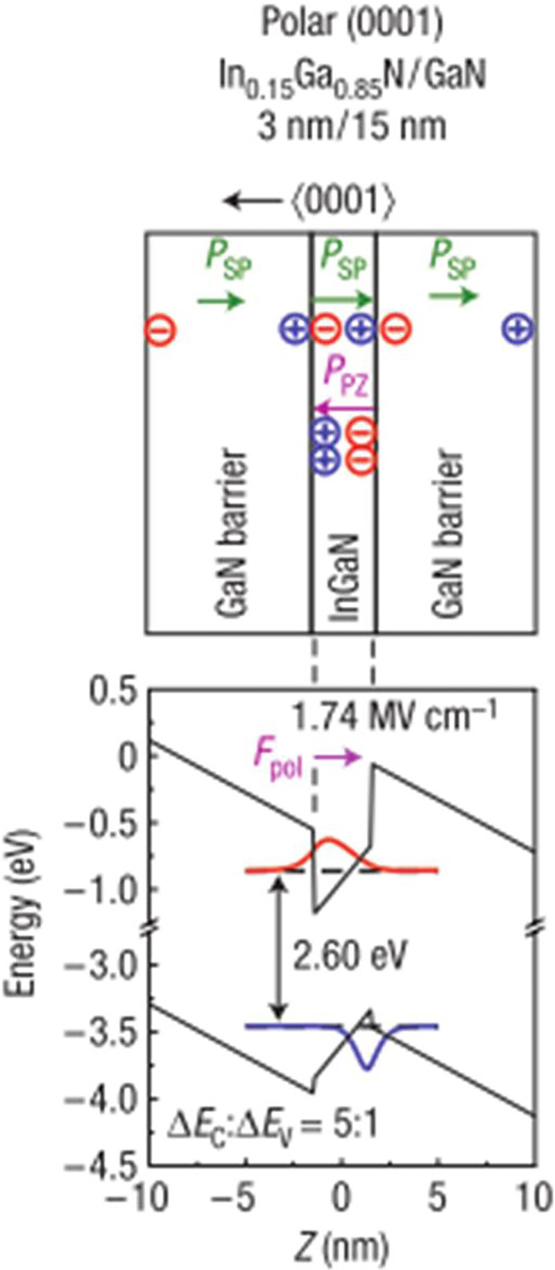
Illustration of polarisation fields and band profile for In0.15Ga0.85N/GaN QW; note tilted bands of both QW and QBs due to polarisation fields; polarisation charges appear at interfaces due to spontaneous polarisation Psp and piezoelectric polarisation Ppz (Ref. 14)
Polarisation effects in LED devices
The following sections will focus on the characterisation of polarisation induced effects on the optoelectronic properties of III-nitride heterostructures rather than their direct measurement through methods such as electron holography, which have previously been demonstrated for various structures such as InGaN QWs,24,25 AlGaN/GaN/InGaN diodes 26 and at dislocation cores.27,28
Bandgap narrowing and power dependent emission blue shift
The spatial separation of the carriers in a triangular QW has several consequences on the emission properties of the LED. In this section, we will discuss how the rhombic or ‘sawtooth’ shape of the QW results in the energy of the optical transition being reduced, which is known as bandgap narrowing that causes a red shifted emission wavelength.
The majority of early experiments reporting the effects of bandgap narrowing in III-nitrides consisted of photoluminescence (PL) experiments, whereby carriers are generated using incident illumination and recombine to emit light. As the bandgap narrowing effect is due to the polarisation fields present in nitrides, it stands that the presence of carriers effectively nullifies this effect by screening the culpable electric fields. The effects of the QCSE in III-nitride QWs were first reported by Takeuchi et al. 29 The authors compared the PL spectra of a structure containing multiple InGaN QWs with those of another structure consisting of a single bulk InGaN layer with increasing illumination power. The results are shown in Fig. 7.
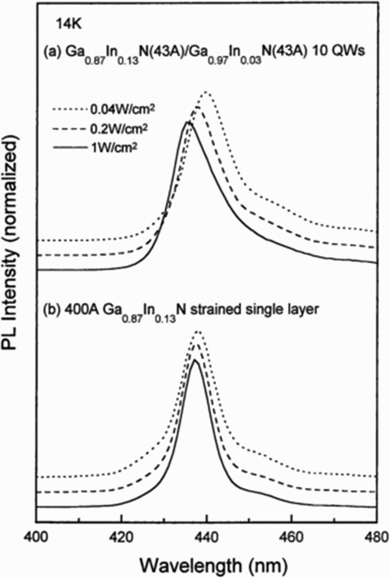
Photoluminescence spectra of a multiple QW structure and b single InGaN layer with increasing excitation power; spectra for QW structure exhibit blue shift in peak emission wavelength with increasing excitation power, while bulk layer spectra remained largely unchanged 29
The blue shift experienced by the QW structure indicates the screening of the polarisation fields by carriers generated by the incident light. 30 The original peak emission wavelength of the QW structure is initially red shifted relative to the bulk InGaN epilayer due to the tilting of the QW energy bands, which results in bandgap narrowing due to the piezoelectric field 29 as shown in Fig. 7.
Although power dependent measurements are an effective way of probing the effects of bandgap narrowing, an equally useful way is to examine the time dependence of the effects of carrier screening. Kim et al. used this approach by employing time resolved PL spectroscopy to study the QCSE and the effect of carrier screening in GaN–AlGaN QWs. By taking PL spectra at different delay times after an initial picosecond excitation pulse, the authors observed a substantial red shift in peak emission wavelength with increasing delay, indicating a ‘recovery’ of the original QCSE in the QWs after initial screening by photoexcited carriers as shown in Fig. 8. 31
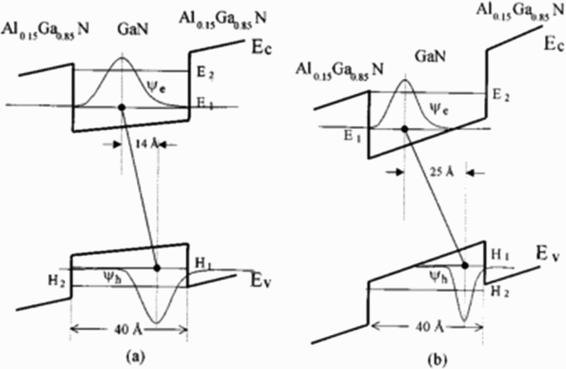
Energy band diagrams of GaN–AlxGa1 − xN QW a under influence of screening by photogenerated carriers at time td = 0 and b after long delay time, returning to original piezoelectric field that causes increased tilting of QW bands and increased spatial separation of carrier wavefunctions 31
As an alternative to carrier bandgap screening through power or time dependent PL experiments, it has been shown that electrically contacting and biasing III-nitride LED structures is perhaps a more direct method of evaluating the effect of the piezoelectric fields on bandgap narrowing as it no longer relies on the injection of carriers for field screening but instead directly affects the tilting of the band structure. Takeuchi et al. used this approach and examined electrically contacted p–i–n InGaN–GaN QW structures. Photoluminescence spectra at increasing reverse bias were examined with an enhanced blue shift observed. 32 The results are shown in Fig. 9.
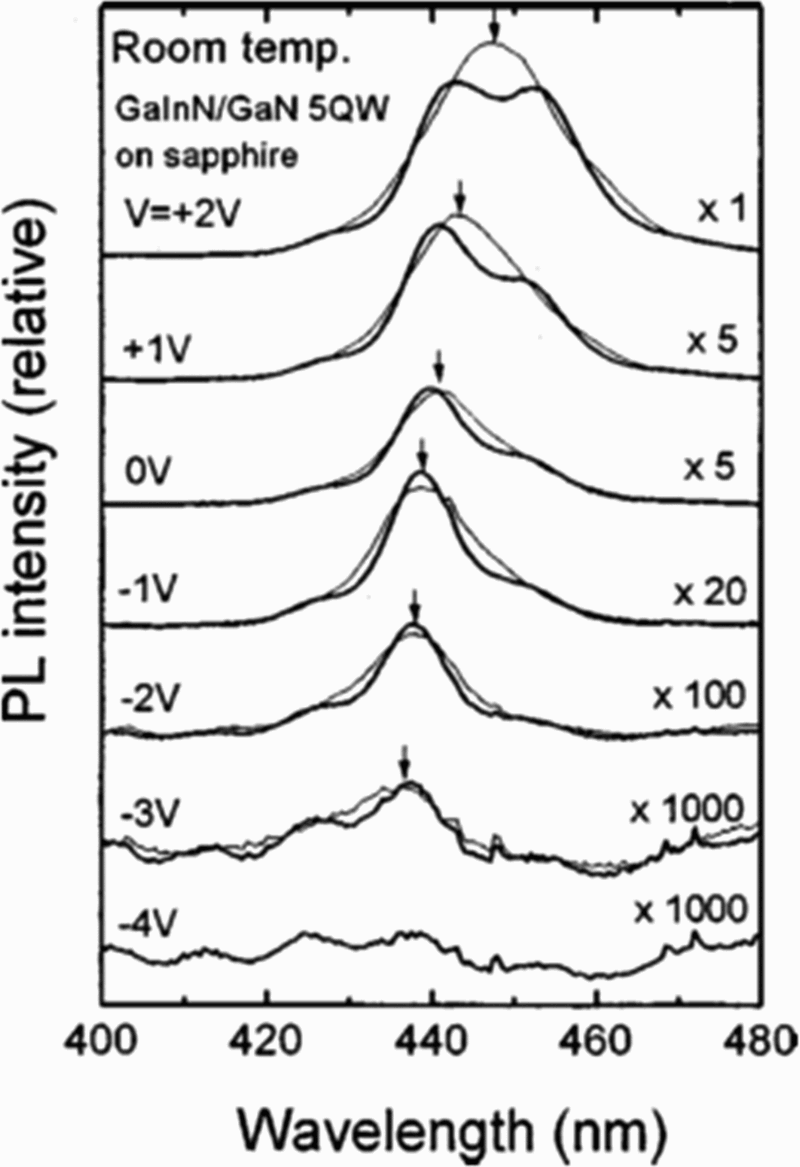
Photoluminescence spectra of In0.16Ga0.86N/GaN p–i–n structure with increasing reverse bias; thin lines represented data fitted to remove interference fringes, and raw data are denoted by thick lines; under reverse bias, p–i–n structure is more likely to generate photocurrent upon illumination rather than subsequent PL, hence dramatic reduction in PL intensity; peak positions of spectra are shown by arrows 32
The observed relationship between peak emission blue shift and increasing reverse bias can be interpreted by considering the effect of the reverse bias on the energy bands of the QW. A reverse bias actually serves to tilt the energy bands of the QW towards the so called ‘flatband condition, where the influence of the piezoelectric effect has been nullified. 32 As a result, the reverse bias causes blue shift in the QW emission energy.
Given the aim of LEDs is to produce light under electrical bias, or electroluminescence (EL), it is important to consider the effect of electrical injection on the polarisation fields. Epitaxial structures for III-nitride based LEDs are typically grown with the p type layer last due to well documented difficulties with p type doping33–36 and thus function under forward bias conditions. Interestingly, the application of a forward bias should have the opposite effect on the QW energy bands to the one observed by Takeuchi et al. 32 if one ignores the effects of carrier screening. On the contrary, increasing the forward bias on a p–i–n InGaN–GaN QW LED structure results in a blue shift in the peak EL spectrum for III-nitride layers grown along the [0001] direction. 37 This blue shift is attributed to the same effect observed for PL under increasing excitation power: 29 increasing bias allows for the injection of a greater number of free carriers into the QW, which in turn result in the partial screening of the QCSE inducing a blue shift in peak emission wavelength. 21
Reduction in oscillator strength and efficiency
The spatial separation of carriers due to the polarisation fields in III-nitride heterostructures results in a decreased probability for radiative recombination or a reduction in oscillator strength. The concept of oscillator strength expresses the probability of interaction between the energy levels of a system and electromagnetic radiation. In essence, the oscillator strengths for a QW determine its emission and absorption properties: 38 the stronger the oscillator for a particular transition, the more likely it is to occur. 39 The oscillator strength of a system can be experimentally inferred as it is directly related to the rate of luminescence decay: a strongly emitting oscillator results in fast decay of the luminescence due to the high transition probability.
As we have noted in the previous section, the effect of the QCSE from the polarisation fields in III-nitride QWs is to transform the QW into a triangular potential and thus spatially separate the electron and hole wave functions. This is exacerbated for thicker wells, as demonstrated in Fig. 10.
Thicker QWs in III-nitrides result in larger spatial separations of electrons and holes and reduced oscillator strength
This effect was used by Im et al. to examine the reduction of oscillator strength in AlGaN/GaN. 40 Thicker wells were first observed to have higher peak emission wavelength relative to the GaN bandgap, an indication of the bandgap narrowing effect previously discussed. The luminescence lifetime of the red shifted emission from the thickest well (10 nm) was observed to be 3 μs, a factor of 104 longer than the decay times for the thinner wells.
Chichibu et al. reported similar effects for InGaN–GaN QWs of varying thickness, noting that the decay times for PL were strongly QW thickness dependent 41 as shown in Fig. 11.
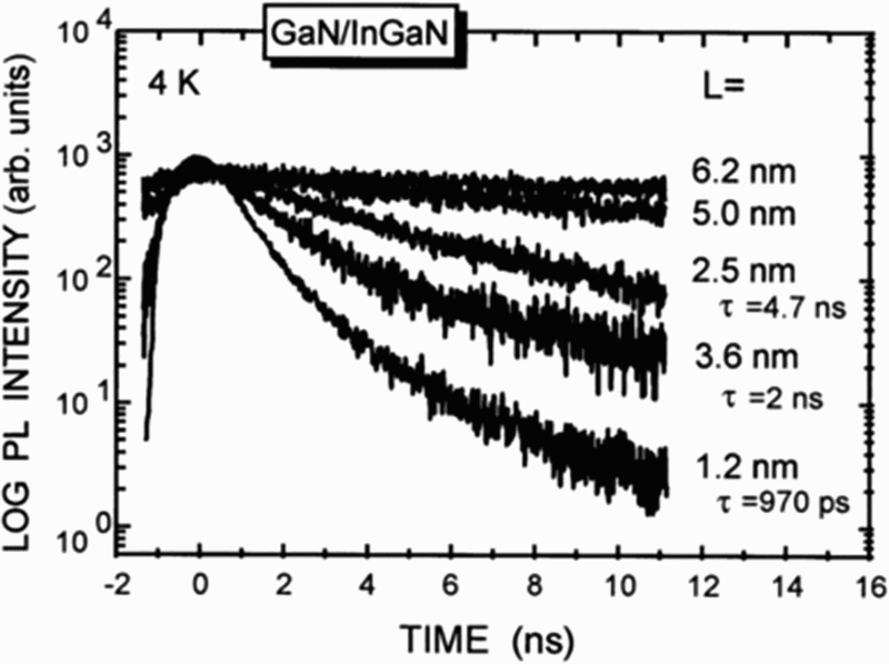
Time resolved PL decay curves for varying well thickness; 5.0 and 6.2 nm thick QWs showed decay lifetimes far beyond range of x-axis; 41 it is clear that thinnest well exhibits fastest decay time and thus highest oscillator strength
The reduction in oscillator strength has significant consequences in terms of LED device efficiency. Radiative and non-radiative processes are in competition; thus, if the radiative lifetime is increased, free carriers are far more likely to recombine non-radiatively at defects. 42 This severely hinders LED device efficiency, particularly in the long wavelength spectral ranges as will be discussed later.
The issue of efficiency ‘droop’ or the fall-off of III-nitride LED efficiency can also be related to this reduction in oscillator strength. Although the origin of efficiency droop is disputed,43–45 it is clear that it occurs for increasing injection carrier density. As such, it would be desirable to grow LED devices with wider QWs in order to reduce carrier density in the wells during operation and thus alleviate the efficiency droop. 46 However, the presence of thicker wells would cause even further separation between carriers in the case of polar LEDs, reducing the radiative recombination probability and thus device efficiency even further.
Mitigating the QCSE
Alternative growth planes
One method to circumvent the deleterious effects of internal fields in III-nitride heterostructures is to redirect the biaxial stress (which is responsible for the piezoelectric polarisation field) along another crystal plane.
47
The electric field vanishes entirely for facets perpendicular to the {0001} plane (c plane) such as the  or
or  planes (a and m planes respectively).
The relationship between crystal angle relative to the c plane, piezoelectric polarisation and carrier wave function overlap for a 3 nm thick In0.25Ga0.75N QW pseudomorphically strained to the GaN QBs is illustrated in Fig. 12.
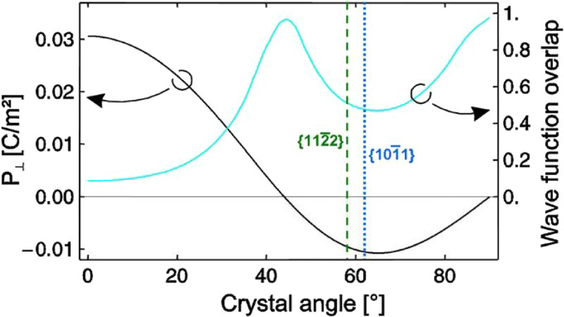
Piezoelectric polarisation (right axis/black curve) and relative carrier wavefunction overlap (left axis/black curve) for 3 nm thick InGaN QW with respect to crystal angle relative to c plane; semipolar planes are shown by dashed line at angle of ∼60° (Ref. 4)
The a and m planes are thus denoted as ‘non-polar’ due to the vanishing polarisation fields along the growth direction. Alternative GaN growth orientations are shown schematically in terms of a GaN unit cell in Fig. 13.
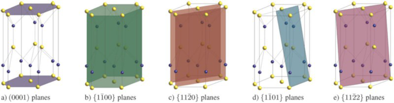
GaN surface orientations: a c plane, b m plane, c a plane, d and e semipolar planes; gallium atoms in yellow/light and nitrogen in blue/dark 48
a plane growth
a plane GaN is almost exclusively grown by MOVPE. The most commonly used substrate is r plane sapphire due to its readily available nature and its well established epitaxial relationship with GaN. 4 The low crystal quality of a plane GaN grown by MOVPE remains one of the primary obstacles to establishing a plane GaN as a viable non-polar alternative to c plane GaN for LED devices. 49 Typical values of stacking fault densities and dislocation densities are in the range of 5 × 105 cm− 1 and 109 cm− 2 respectively. On the other hand, dislocation densities on the order of 108 cm− 2 are easily achievable for c plane GaN, with even lower values achievable using defect reduction techniques.5,50 Stacking faults are less of an issue in c plane GaN as they lie perpendicular to the growth direction and can be overgrown by fault free material. 4 Techniques such as the use of low temperature GaN 51 and high temperature AlN nucleation layers52–54 have shown fruitful results in the case of improving polar III-nitride growth. Similar approaches have also resulted in some limited improvements to a plane GaN layer qualities. 55 However, the technique yielding the greatest improvement in material quality is epitaxial lateral overgrowth (ELOG), as shown schematically in Fig. 14.
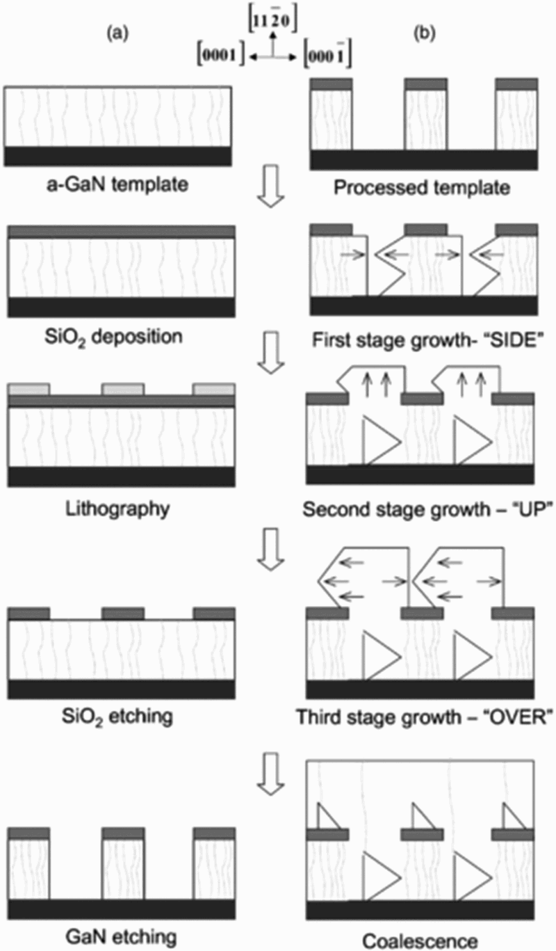
a template lithography and b sidegrowth and overgrowth for the sidewall epitaxial overgrowth (SLEO) process for a plane GaN 56
In the SLEO process, a GaN buffer layer is first grown and covered with a dielectric mask, which is then patterned using optical lithography. As the epitaxial growth is continued, the GaN grows laterally (along the [0001] direction) out of the defined openings and coalesces. This method results in a considerable reduction in defect densities in the epitaxial film.
Early attempts at growing a plane LED devices were plagued by the effects of large defect and stacking fault densities. Chitnis et al. reported a slow turn-on for an a plane GaN–InGaN QW LED structure, most likely due to the presence of dislocations and stacking faults as leakage conduction pathways. 57 Using an ELOG approach and low defect density HVPE grown templates, Chakraborty et al. produced a plane LED structures with improved current–voltage characteristics, with relatively intense emission at a peak wavelength of 413 nm independent of drive current, as expected of non-polar LED structures. 58
Rather ironically, a plane LED devices for emission at longer wavelengths are particularly afflicted by material quality issues as reduction of the bandgap narrowing effect requires the incorporation of higher indium compositions within the QWs to achieve longer wavelength emission. 4 This is even further exacerbated by the apparent inefficient incorporation of indium into a plane GaN relative to the c plane layers 59 and semipolar facets in surface pits. 39 As such, a plane growth is considered suboptimal for the development of high performance LEDs despite its nature as a non-polar solution. 49
m plane growth
In terms of III-nitride, crystal quality growth along the m plane is considered far more promising than that along the a plane. 4 Waltereit et al. reported the first instance of an m plane AlGaN/GaN LED structure grown by rf plasma assisted molecular beam epitaxy on a tetragonal LiAlO2 (LAO) substrate, demonstrating both a decreased luminescence decay lifetime and a luminescence blue shift relative to a c plane QW structure of the same well width as shown in Fig. 15 (Ref. 14).
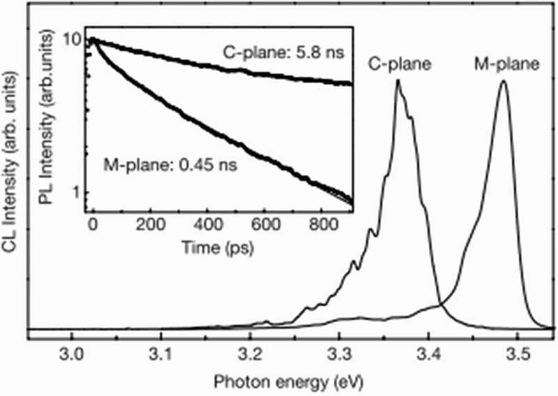
Cathodoluminescence spectra of c plane and m plane QW structures; inset shows luminescence decay curves; m plane QW structure is both blue shifted and exhibits stronger oscillator strength and thus faster luminescence decay, as expected for non-polar structures 14
LAO has been considered a favourable candidate for the growth of non-polar III-nitrides due to its small lattice mismatch with m plane GaN (0.3–1.7 depending on the direction). 61 Mauder et al. also reported promising results in the form of extremely low stacking fault densities for MOVPE grown m plane GaN on LAO; 61 however, it has been observed that the high growth temperatures and ambient hydrogen characteristic of MOVPE growth induce damage to the LAO substrate, resulting in large background carrier concentrations, rough surfaces and broad PL emission spectra, 61 all undesirable features for LED growth. It has been hypothesised that substrate damage is the direct cause for the poor performance of m plane LED structures grown by MOVPE on LAO. 62
As an alternative, m plane silicon carbide (SiC) has also been considered as a substrate for m plane growth of GaN. However, as is typical of the heteroepitaxial growth of non-polar GaN, large stacking fault densities (∼106 cm− 2) have been reported for the growth of m plane GaN on SiC, thus requiring the need for techniques such as graded AlGaN layers 63 or SLEO to reduce defect densities. 64 It should be noted that lateral epitaxial overgrowth techniques are considered effective in reducing threading dislocation density but are far less effective for stacking faults for non-polar growth of GaN.65,66
The introduction of bulk GaN crystals grown by HVPE for non-polar growth marks a turning point in the development of non-polar LEDs. III-Nitride QW structures grown on foreign substrates had until then demonstrated large defect densities, even with the use of ELOG techniques, resulting in particularly poor LED device performance with output powers an order of magnitude (below 1 mW at 20 mA drive current) weaker than high performance c plane devices. 49 Okamoto et al. demonstrated the first milliwatt level blue m plane LEDs by growing the structures on HVPE GaN substrates cut towards the m direction. 67 Shortly thereafter, non-polar growth on cut free standing bulk GaN substrates was used to produce m plane LEDs emitting at 407 nm with an output power of 23.7 mW at 20 mA. 68
Despite the reduction of extended defects in m plane GaN through the use of free standing HVPE bulk substrates for growth, device performance beyond the emission wavelength of 500 nm remains hindered by issues with indium incorporation. 49 Detchprohm et al. reported a difference in output power close to two orders of magnitude between m plane LED structures emitting at 490 and 510 nm. 69
The origin of the dramatic drop in output power with increasing peak emission wavelength has been attributed to the presence of basal plane stacking faults (BSFs) bounded by partial dislocations known as type I1 BSFs by Wu et al. 70 These partial dislocations act as non-radiative recombination centres, hindering light emission from the LED structure. Transmission electron microscopy (TEM) images were taken for two QW widths (2.5 and 4 nm) for which the corresponding LEDs showed an order of magnitude difference in light output power at 20 mA injection current 71 and demonstrated a clear difference in dislocation and stacking fault densities as shown in Fig. 16.
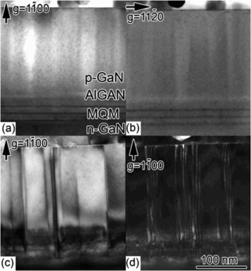
Cross-sectional TEM images along two diffraction conditions for 2.5 nm thick QW LED structure (a and b), c bright field TEM image, and d dark field image for 4 nm thick QW; stacking faults and dislocations can easily be observed for 4 nm thick QW sample 70
Furthermore, Wu et al. demonstrated that the BSFs and partial dislocations originated from the InGaN QWs in the structure and not from the substrate, where the dislocation density was far lower than the density calculated from the TEM images. 70
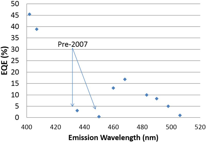
As such, while m plane growth remains far more promising than a plane in terms of non-polar LED structures, material issues such as the generation of BSFs and partial dislocations tend to persist when longer emission wavelengths are targeted. Figure 17 demonstrates that the highest EQEs have been achieved for m plane devices in the blue spectral range. Although it is unlikely that m plane will compete directly with c plane LEDs in this range, 75 reports of reduced efficiency droop at large injection current for m plane LEDs relative to c plane devices indicate that m plane devices may be successful as high efficiency devices at high drive currents. 76 However, the requirement for expensive bulk cut HVPE grown GaN templates for acceptable crystal quality remains a hindrance in terms of the commercial and industrial viability of non-polar LED growth.
Semipolar growth
Interest in semipolar growth orientations has stemmed from the apparent ∼500 nm emission wavelength limitation for m plane devices. Semipolar III-nitride heterostructures have also been shown to exhibit reduced internal fields relative to c plane heterostructures 77 and hence represent a compromise between the deleterious effects of polarisation fields in polar heterostructures and BSF formation in long wavelength non-polar devices. 49
Initial efforts for growth of GaN on m plane sapphire resulted in twinned growth along the  direction.
78
It was subsequently found that sapphire nitridation
79
and optimisation of temperature and pressure during growth
80
are crucial to suppress twinned
direction.
78
It was subsequently found that sapphire nitridation
79
and optimisation of temperature and pressure during growth
80
are crucial to suppress twinned  growth and favour
  GaN growth, resulting in smoother surfaces.
80
Johnston et al. demonstrated the use of a scandium nitride (ScN) layer in improving
GaN growth, resulting in smoother surfaces.
80
Johnston et al. demonstrated the use of a scandium nitride (ScN) layer in improving  GaN crystal quality by reducing dislocation and BSF densities,
81
a technique already known for c plane growth on r plane sapphire.
82
In the case of
GaN crystal quality by reducing dislocation and BSF densities,
81
a technique already known for c plane growth on r plane sapphire.
82
In the case of  GaN, lateral overgrowth techniques have also been shown to improve crystal quality by reducing stacking fault density.
83
GaN, lateral overgrowth techniques have also been shown to improve crystal quality by reducing stacking fault density.
83
The first demonstration of a semipolar InGaN/GaN LED was reported by Kamiyama et al., with a reduced blue shift in peak emission wavelength with increasing injection current relative to a reference c plane LED structure observed.
84
Following this, Chakraborty et al. produced the first semipolar LEDs on free standing  and
and  HVPE GaN templates that exhibited drive current independent peak emission wavelength at 439 nm (blue).
85
As was the case with non-polar LED structures, the performance of semipolar LEDs was greatly enhanced through the use of substrates cut from bulk c plane GaN grown through HVPE.86–90
HVPE GaN templates that exhibited drive current independent peak emission wavelength at 439 nm (blue).
85
As was the case with non-polar LED structures, the performance of semipolar LEDs was greatly enhanced through the use of substrates cut from bulk c plane GaN grown through HVPE.86–90
The apparent higher indium incorporation of the  plane relative to the m plane has enabled the growth of LED structures in the green (516 nm)
91
and yellow (562.7 nm)
92
spectral ranges, a feat unattainable using m plane growth due to the formation of BSFs. The origin of the higher indium incorporation has been reported to be the reduced strain–repulsive interactions of indium atoms in GaN on the
plane relative to the m plane has enabled the growth of LED structures in the green (516 nm)
91
and yellow (562.7 nm)
92
spectral ranges, a feat unattainable using m plane growth due to the formation of BSFs. The origin of the higher indium incorporation has been reported to be the reduced strain–repulsive interactions of indium atoms in GaN on the  plane relative to the m plane.
93
plane relative to the m plane.
93
Presently, semipolar growth along the  and
and  planes has yielded the most promising results in terms of long wavelength device performance.
49
It has been demonstrated that indium incorporation along the
planes has yielded the most promising results in terms of long wavelength device performance.
49
It has been demonstrated that indium incorporation along the  plane is particularly efficient relative to other non-polar and semipolar facets; furthermore for
  p–n structures, the built-in field and polarisation induced field are subtractive, resulting in a more rectangular and thus desirable QW potential profile compared to
  QW structures.
 plane multiple QW LED structures have also been shown to exhibit improved hole transport relative to
  plane MQW LEDs.
95
It has also been reported that the
plane MQW LEDs.
95
It has also been reported that the  plane exhibits a higher optical polarisation ratio relative to the
  plane.
96
plane.
96
There have been several reports of  LEDs grown cut substrates with favourable performance in the green (∼515 nm) and yellow green spectral range (∼550 nm).97–99 It has been suggested that the more uniform indium incorporation along these planes for InGaN QW growth results in low spectral blue shift with increasing injection (due to localisation related effects) and a narrow spectral linewidth relative to other growth planes, both desirable properties for LEDs.
The EQEs reported in Ref. 97, 20 at 516 nm and 12.6 at 552 nm for drive currents of 20 mA, compare very well with efficiencies reported in the literature for c plane devices emitting at similar wavelengths where sub-10 EQEs have been reported although no corresponding drive current has been given for these EQEs.100,101 While it is important to note that it is very difficult to directly compare EQE values given without a corresponding drive current and that EQE can be dependent on light extraction from the LED and other factors outside the internal quantum efficiency, the given values for semipolar LEDs emitting in the green and green yellow spectral ranges seem very encouraging.
Semipolar LEDs may be useful for operation in the blue spectral range where c plane devices exhibit extremely high EQEs (∼84) 75 but also severe efficiency droop. 44 The ability to grow larger QWs relative to polar LEDs allows for the reduction in carrier density and thus efficiency droop and has been reported to consequently allow for reduced droop at high drive currents 102 as shown in Fig. 18, as well as a reduction in thermal droop. 103 One could thus foresee an application for semipolar LEDs in high brightness low area LED applications. 74

Comparison of internal quantum efficiency for a
(Ref. 102), b c plane.
75
and c c plane;
104
all devices emit at ∼450 nm (blue); although c plane devices exhibit higher efficiencies at lower current densities, reduction of efficiency droop allows semipolar LED to exhibit higher efficiencies at large current densities
46
Despite these promising results, issues inherent to the heteroepitaxial growth remain in the implementation of semipolar LED devices. The prohibitive price of bulk GaN substrate cutting remains a key issue to be overcome before semipolar and non-polar LEDs can compete commercially with current c plane LEDs in terms of production costs.
Doping
The intentional incorporation of impurities in III-nitrides has been reported to provide beneficial control of the QCSE. It has been suggested that this is achieved through several mechanisms that shall be discussed in this section.
There is a wealth of evidence suggesting that doping the QBs increases oscillator strength and reduces bandgap narrowing through free carrier screening of the QCSE,105–107 Di Carlo et al. used self-consistent tight binding calculations to demonstrate a blue shift in the optical transition energy for highly doped barriers in AlGaN–GaN QWs that was more prominent at lower injected carrier density, consistent with the idea of dopant screening rather than injected carrier screening. 106 Choi et al. studied a series of InGaN/GaN QW structures with various doping levels to determine that the piezoelectric fields in the QWs were screened from Si donors in the barriers due to a reduction in Stokes shift with increasing doping level. 105 Esmaeili et al. reported the effect of doping on AlGaN/GaN QW structures by establishing that the screening effect of photogenerated carriers in their PL study was minimal in moderately and heavily doped samples, indicating that the carriers originating from the doped barriers dominated the screening effect in these samples rather than injected carriers. 107
Some reports indicate that carrier localisation through QW width fluctuations or indium content fluctuations is also responsible for the perceived blue shift in PL. It has been suggested that the introduction of silicon doping can cause the InGaN QWs in some structures to undergo strain relaxation by decomposing,108,109 thus creating localisation centres and enhancing radiative efficiency. However, it is important to note that these results implying the generation of high indium content clusters were obtained by strain state analysis of TEM images, a technique O'Neil et al. and Smeeton et al. showed to be particularly susceptible to false detection due to strain induced by the imaging method itself,110,111 and indeed, it has been suggested that the optical properties of InGaN QWs may be influenced by ordering rather than clustering. 112 Furthermore, it has been shown that localisation of carriers can be induced by random indium alloy fluctuations as well as monolayer QW thickness fluctuations in undoped QW structures without the presence of gross indium clusters, 113 thus casting some doubt over claims that silicon doping can induce indium clustering and be responsible for higher radiative efficiency.
Despite the numerous PL studies that indicate that doping can help alleviate symptoms of the QCSE, it is also important to consider the effect this can have on the electrical properties of an LED. The excessive silicon doping of QBs can, in fact, exert a ‘hole blocking effect’ on the whole structure, hindering the transport of positive carriers throughout the structure, 114 which can result in a significant decrease in EL intensity. 115
Strain control
The piezoelectric component tends to dominate the internal fields for (0001) InGaN/GaN QWs, and as such, an effective method of reducing the deleterious effects of the QCSE in these structures is to control the strain in the QW layer by manipulating the strain states of adjacent layers. 30
Nanhui et al. investigated the effect of strain relaxation on the optoelectronic properties of InGaN/GaN QW structures through the growth of InGaN underlayers intended to act as strain relief layers. 116 The authors reported a twofold increase in PL intensity for the structure with the underlayer relative to the control structure and a blue shift in peak emission wavelength, attributed to the partial relaxation of strain in the QW layer. Furthermore, the density of V pits, whose formation is commonly attributed to strain relaxation, was reduced from 16–18 × 108 to 6–7 × 108 cm− 2. A further study by the authors revealed a decrease in the maximum blue shift between low and high current densities for the strain relaxed samples grown on InGaN/GaN superlattices relative to the standard QW structure. 117
While the addition of an underlayer can help manage strain, it is also possible to change the layers grown above the active region to engineer strain. Ryou et al. reported a reduced blue shift with increasing injection current in a structure with a p-InGaN layer relative to a structure with a p-GaN layer. 21 The authors also reported considerably higher peak EL intensity for the p-InGaN structure. Both the reduced blue shift and the increased EL intensity were attributed to the reduction of compressive strain on the InGaN QW by employing a p layer with lower lattice mismatch to the QWs.
More recently, van den Broeck et al. reported strain balancing through the use of a thick InyGa1 − yN template for the growth of InxGa1 − xN/GaN QWs, where x>y. 118 The template used was grown far beyond the critical layer thickness to ensure full relaxation. As such, the active region of QWs grown on this relaxed layer was strained to the lattice constant of the template rather than of the GaN substrate, as shown in Fig. 19.
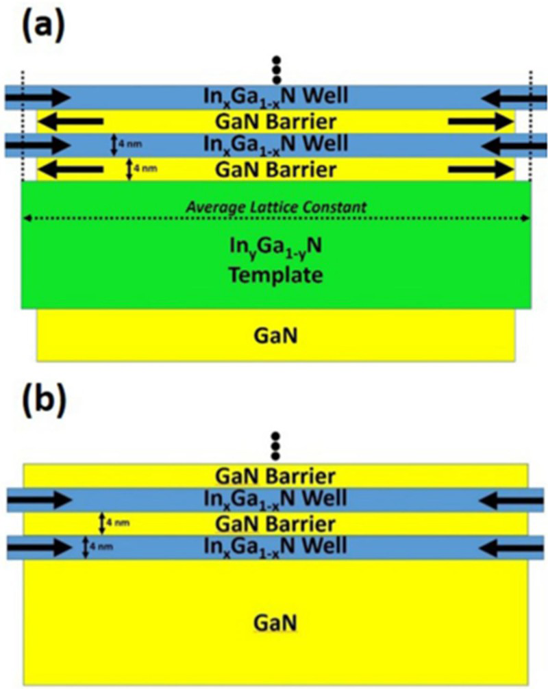
a strain balanced InGaN/GaN structure grown on lower indium content InGaN template and b conventional QW structure on GaN 118
This approach leads to compressive strain on the InGaN wells and tensile strain for the GaN barriers. By optimising the indium content of the QWs and the strain balancing template, the authors reported fully strain balanced structures, with no strain relaxation effects observed for increasing number of QWs grown on the balanced templates. Furthermore, the strain balanced structures exhibited higher emission intensity, indicative of a reduction in the strain induced piezoelectric field.
It is also important to note the effect of strain on indium incorporation for III-nitride structures when considering strain as a method of controlling the QCSE. Pereira et al. used depth resolved cathodoluminescence, Rutherford backscattering spectrometry 119 and X-ray reciprocal space mapping 120 to demonstrate that the strain can obstruct the incorporation of indium atoms in an InGaN lattice. As such, the design of devices emitting at longer wavelengths requires careful consideration if strain relaxation techniques are used to control the QCSE as the interplay between strain, indium incorporation and emission wavelength must be taken into account.
Cubic III-nitrides
Zinc blende (cubic) III-nitrides offer an alternative way of eliminating polarisation fields inherent to their wurtzite counterparts. Recently, interest in cubic III-nitride growth can be attributed to several factors: cleaving (001) oriented zinc blende GaN along the vertical {110} plane, 121 enhanced p type carrier mobility 122 and of course the removal of polarisation fields. Cubic InGaN/GaN QW structures are also expected to have the additional advantage of an inherently lower bandgap, thus requiring a lower indium composition for long wavelength devices. 123
Cubic III-nitride growth has been demonstrated on (0 0 1) GaAs, 124 (0 0 1) Si, 125 sapphire and (1 1 1) GaAs. Li et al. demonstrated room temperature green light emission from LED cubic InGaN/GaN QWs grown on 3C–SiC substrates and reported increasing PL intensity for larger well widths, indicating the absence of polarisation fields. 126 More recently, Stark et al. demonstrated EL from cubic InGaN/GaN LED structures grown on structured V grooves in Si (1 0 0) substrates and reported injection current independent emission wavelength, with few line defects or wurtzite inclusions within the cubic GaN. 127 Despite this, the difficulty of growing cubic GaN can be seen from the rough and discontinuous surface shown in Fig. 20.
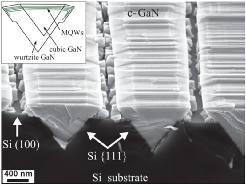
Scanning electron microscopy image of cross-section of cubic InGaN/GaN QWs grown on patterned Si (1 0 0) substrate; ‘V’ shaped boundary between wurtzite and cubic GaN can be seen from image contrast 127
While the development of cubic GaN does have many potential advantages for LED structures, the necessity for additional processing steps due to the higher thermodynamic stability of wurtzite GaN and the lack of material yield and quality renders this method of mitigating polarisation fields less attractive from an industrial and commercial point of view.
Conclusions
III-Nitride LEDs have already revolutionised the lighting industry, allowing for unprecedented energy savings on a global scale. However, in order to further improve their performance, the impact of the polarisation fields inherent to these materials must be controlled. This review has outlined the deleterious effects of polarisation fields on the emission properties of III-nitride QWs and several methods of controlling these detrimental effects.
In many cases, advances in device development have been swift, but a full understanding of the unique material challenges in controlling the polarisation fields for LEDs has been slower to materialise. Particularly in the case of alternative growth planes, considered the most promising method of mitigating the QCSE, the reduction of BSFs and high quality heteroepitaxial growth remain a priority and are the main obstacles preventing non-/semipolar LEDs from being commercially viable.
At present, it seems that semipolar growth for the mitigation of polarisation fields seems to be the most successful approach, particularly for long wavelength LEDs. These have demonstrated high efficiencies and low efficiency droop, although the efficiencies demonstrated in the blue spectral wavelength still lag behind those of c plane LEDs at lower injection currents. However, there is a distinct lack of comparison between efficiencies reported in the literature for LEDs grown on alternative growth planes, using strain or doping engineering, and normal c plane. A consistent method of comparison, whether it be for the same target emission wavelength, indium compositions or drive current, is required in order to truly assess the success of polarisation field mitigation techniques.
The strong impact III-nitride LED research continues to have commercially and industrially is perhaps best highlighted by this: although high performance devices may be achieved using various methods discussed throughout this review, a key consideration remains the feasibility of commercialisation, without which the development of a device cannot be considered a complete success.
Footnotes
Acknowledgements
Many thanks to Dr. Rachel Oliver for her supervision and valuable advice. I would also like to thank James Griffiths, Thomas O'Hanlon, Helen Springbett, An Bao, Thomas Choi, Dr. Tim Puchtler, Spark Zhang and Dr. Fabien Massabuau for invaluable discussions and enthusiasm in the office. The EPSRC Cambridge/UCL Photonics CDT and ERC MaCONS grant are gratefully acknowledged for financial support.
References
 InGaN/GaN light-emitting diodes with low efficiency droop at 200 A/cm2’
 bulk GaN substrate’
 bulk GaN substrates’
 surfaces: group-III adlayers and indium incorporation’
 and
and  multiple-quantum-well light-emitting diodes’
 blue-green InGaN/GaN light-emitting diodes’
 GaN substrates’
 InGaN/GaN light emitting diodes with various wavelengths’
 InGaN light-emitting diodes with small wavelength shift and narrow spectral linewidth’
 single-quantum-well blue light-emitting diodes, Appl’
 blue light-emitting diodes’