
Abstract
An orthogonal experiment scheme was employed to study the influences of forming pressure, sintering temperature and holding time and Cu content on microstructure, hardness and electrical resistivity of the Cu/Invar composites prepared by the powder metallurgy (PM) technique. The interdiffusion of the Fe, Ni and Cu atoms of the composites during sintering was also investigated. The results show that the Invar alloy is distributed continuously in the composites, when the Cu content is 30 wt-% and below; when the Cu content is 40 wt-% and above, a continuous net structure of Cu forms. Properties, especially the electrical and thermal conductivities, depend on the relative density and atom interdiffusion of the Cu/Invar composites. Taking the electrical resistivity of the composites as index, the optimum processing parameters are: forming pressure of 600 MPa, sintering temperature of 1000°C, holding time of 60 min and Cu content of 50 wt-%.
Keywords
Introduction
Since the first semiconductor integrated circuit (IC) was developed in 1958, integrated levels of the IC chips have been enlarged several times over till now. It correspondingly makes more and more demands on the electronic packaging materials.1–3 Unfortunately, any single-phase material in the world cannot meet all of the performances of an ideal electronic packaging material, so far. 4 For those commonly-used electronic packaging materials, Cu and Al have high thermal conductivities, low cost and good processabilities, but their thermal expansion coefficients (CTE) are much higher than those of the Si and GaAs chips, which may induce high thermal stress in the IC devices on service state. Invar (Fe–36Ni) alloy and Kovar (Fe–29Ni–17Co) alloy have low CTEs, consistent with those of the Si and GaAs chips, and good weldabilities and processabilities, but their thermal conductivities are very low. W and Mo have high thermal conductivities and CTEs similar to the Si chip, but their wettabilities and weldabilities are poor. Moreover, high densities and cost of W and Mo also inhibit the application of the metals as the electronic packaging materials. Metal matrix composites of Al/SiCp and Al/Sip have excellent comprehensive properties as the electronic packaging materials, such as the tailorable CTEs, high thermal conductivities and low densities, but the high volumes of SiC or Si in the composites inevitably result in poor processabilities and machinabilities of them. The composites are also difficult to be electroplated or welded.5,6
It is well known that Cu has high electrical conductivity and thermal conductivity, but its CTE is too high. On the contrary, the Invar alloy has very low CTE due to its Invar effect in a certain temperature range. 7 The CTE of the Invar alloy can be further decreased through substituting 4 wt-%Ni in the alloy with Co. The super Invar alloy of Fe–32Ni–4Co has much lower CTE of 0.3–0.5×10⁻⁶°C−1 at the temperature range from 20 to 200°C; 8 however, the thermal conductivity of the alloy is very low. In the authors’ opinion, a novel material of the Cu/Invar composites should be designed as an alternative of the traditional electronic packaging materials of Cu/W (Mo), Kovar, stainless steel and etc, combining the excellent electrical conductivity and thermal conductivity of Cu and the low CTE of Invar alloy. Meanwhile, the composites have good processability and machinability, and are easy to be electroplated or soldered.
Many techniques are technologically employed to prepare the Cu/Invar composites, such as multi-layer laminating, extruding, casting, powder metallurgy (PM), and so on.9–12 Microstructures of the Cu/Invar composites prepared by laminating and extruding are anisotropic. The casting temperature of the composites is so high that the reaction between the Invar alloy and Cu is severe. Both of them are believed to have bad influences on the properties and applications of the composites. Powder metallurgy technique is simple and low cost, more importantly, it can be used to fabricate the Cu/Invar composites at rather lower temperature than casting, and the composites also have isotropous microstructure other than the laminating and extruding processes. In this paper, the Cu/Invar composites were prepared by PM, the process was designed in terms of an orthogonal experimental scheme, and the main processing parameters were optimised, taking the hardness and the electrical conductivity of the composites as indexes, respectively.
Experimental methods
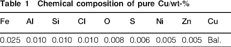
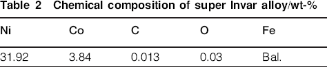
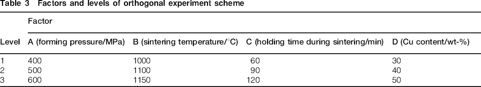
Electrolytic Cu powder with an average particle size below 300 mesh and a purity of 99.9 wt-% was provided by Zhongjinyan New Materials Co. Ltd, Beijing, China. The composition of the Cu powder is shown in Table 1. The Fe–32Ni–4Co Super Invar alloy powder with an average particle size below 200 mesh and a purity of 99.8 wt-% was fabricated in our lab through a gas atomisation technique, its composition is listed in Table 2. The Cu powder and the Invar powder were blended with mass ratios of 30∶70, 40∶60 and 50∶50, in which 0.5 wt-% zinc stearate powder was added as a lubricant agent. After the as blended powder was mixed for 10 h in a plastic container, it was uniaxially compacted with set pressures of 400, 500 and 600 MPa for 2 min, respectively, using a 769YP-40C type powder compressing machine. The composite green bodies were finally sintered at temperatures of 1000, 1100 and 1150°C for holding times of 60, 90 and 120 min, respectively, employing a GSL-1600X type atmosphere protecting furnace. The specimens were heated at a rate of 5°C min−1 and cooled at the same rate to 800°C and then by furnace cooling. The specimens were still protected in the whole sintering period in a H2 atmosphere with a flowing rate of 100 mL min−1. A L9 (3 4 ) orthogonal table (Table 3) was designed to study the effects of Cu/Invar content ratio, forming pressure and sintering temperature and time on microstructures and properties of the Cu/Invar composites in order to optimise the process parameters.
Chemical composition of pure Cu/wt-%
Chemical composition of super Invar alloy/wt-%
Factors and levels of orthogonal experiment scheme
Densities of the sintered Cu/Invar composites were measured, based on the Archimedes principle, and then the relative densities of the composites were deduced. Before the density test, the sintered specimens should be sealed using wax to avoid the effect of the surface pores. Hardness values of the sintered specimens were measured using a HV-10A type Vickers hardness tester with a load of 5 kg and a holding time of 15 s. Electrical resistances of the sintered specimens of 60×8×5 mm in size were examined using an Agilent U3606A type desktop multimeter. Then the electrical resistivities or electrical conductivities of the specimens were determined. Phases of the sintered specimens were analysed using a D/MAX2500V type X-ray diffractometer (XRD). The lattice distortion degrees of the phases in the specimens were confirmed according to the XRD results, and the dissolved amounts of Fe, Ni in Cu and that of Cu in the Invar alloy were calculated, respectively, in terms of the Vegard's law. 13 Microstructures of the sintered specimens were observed using an Olympus optical microscope and a SM6490 type scanning electron microscope (SEM) equipped with an Oxford INCA type energy dispersive spectrometer (EDS).
Results and discussion
Orthogonal experiment
In this work, the performance of the Cu/Invar composites is characterised by taking hardness and electrical resistivity as indexes, respectively. Based on the hardness and electrical resistivity tests, the tensile strength and the electrical and thermal conductivities should be evaluated or calculated in terms of the material science theories and the Wiedermann–Franz formula, 14 respectively.
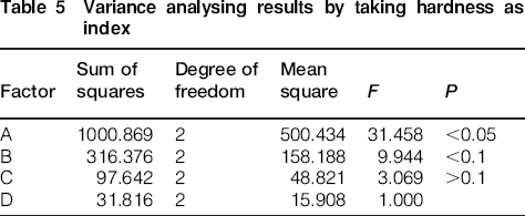
As shown in Table 4, taking the hardness of the composites as index, R values of factor A (forming pressure) are the greatest than all others, indicating that factor A is the dominating one of them. The sequence of these factors is A, B, C and D from high to low with the index of hardness. With the electrical resistivity of the composites as index, the sequence of these factors is changed to be D, A, C and B from high to low. R values of factor D (Cu content) are the largest, suggesting that the Cu content is the main factor. Analyses of variance in Table 5 indicate that F value of factor A is the greatest and that of factor B is the secondary by taking hardness as index; while only factor D has the highest effect by taking the electrical resistivity as index (Table 6).
Results of orthogonal experiment
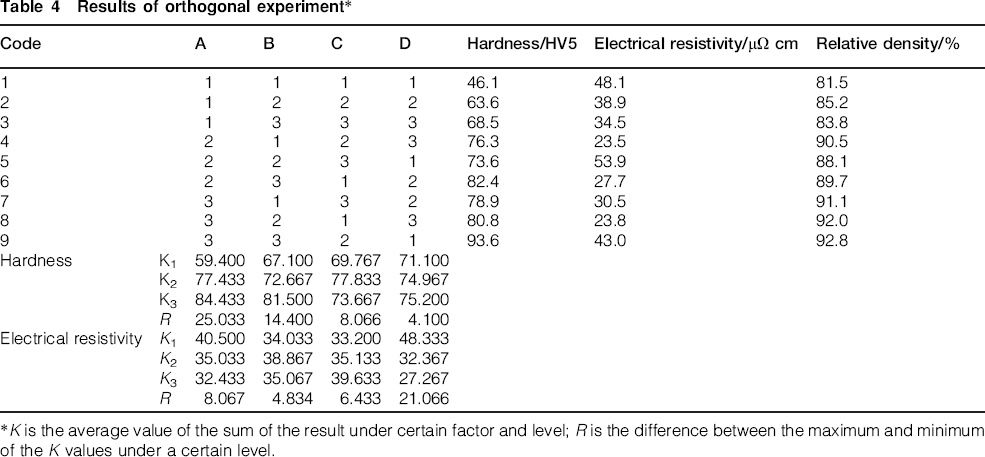
K is the average value of the sum of the result under certain factor and level; R is the difference between the maximum and minimum of the K values under a certain level.
Variance analysing results by taking hardness as index
Variance analysing results by taking electrical resistivity as index
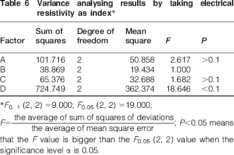
F0. 1 (2, 2) = 9.000; F0.05 (2, 2) = 19.000;
 P<0.05 means that the F value is bigger than the F0.05 (2, 2) value when the significance level α is 0.05.
Certainly, the smaller the electrical resistivity, the better the composites. The best level and factor in the orthogonal experiment is corresponding to the minimum average value of the electrical resistivity. Therefore, the optimal PM process parameters for the Cu/Invar composites are A3B1C1D3, i.e. the forming pressure of 600 MPa, the sintering temperature of 1000°C, the holding time of 60 min and the Cu content of 50 wt-%, respectively. On the other hand, taking hardness as index, the higher the hardness, the better the composites. The optimal PM process parameters of A3B3C2D3 were deduced to be: the forming pressure of 600 MPa, the sintering temperature of 1150°C, the holding time of 90 min and the Cu content of 50 wt-%, respectively, to get the Cu/Invar composites with the excellent mechanical properties.
According to the orthogonal experimental results, the optimal PM process parameters are varied taking different index. Taking hardness as index, the hardness of composites greatly increases with increasing forming pressure. Sample A1B1C1D1 has the lowest hardness of 46.1 HV5, even less than those of pure Cu (58 HV) and Invar (144 HV), due to its lowest relative density. With the increasing forming pressure, the densities and hardness values of the composites increase obviously. In order to decrease the electrical conductivities of the composites, increase in the Cu content and the forming pressure and decrease in the sintering temperature and holding time are recommended.
XRD analyses
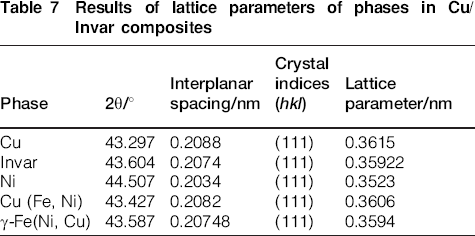
Phase analyses of the as blended Cu/Invar composite powder and the sintered sample A1B1C1D1 are shown in Fig. 1. (111), (200) and (220) peaks of face-centred cubic (fcc) Cu and those of fcc Invar alloy (γ-phase austenite) are marked in Fig. 1a. The Cu (111) peak of the sintered Cu/Invar composite shifts to right (high reflection angle orientation), and the Invar (111) peak moves to left (low reflection angle orientation), respectively, compared with those of the Cu and Invar alloy in the as blended composite powder. In addition, in the reflection angle range between 44 and 45°, the α-Fe (Ni, Co) (110) diffraction peak was detected (Fig. 1b). During sintering the composites, Fe, Ni atoms in the Invar alloy diffuse into Cu and form the Cu (Fe, Ni) solid solution. Because the atomic radii of Fe (0.124 nm) and Ni (0.125 nm) are smaller than that of Cu (0.128 nm), diffusion of the Fe, Ni atoms into Cu leads to the right shift of the Cu peaks. Similarly, the peaks of the γ-phase Invar alloy move a little bit to the left because the larger Cu atoms dissolve into the Invar alloy. Based on the Cu–Fe and Cu–Ni phase diagrams, 15 an infinite solid solution exists in the Cu–Ni binary system, and only definite solid solutions should be formed in the Cu–Fe binary system, the solid solubility of Fe in Cu is only 1.1 wt-% at 850°C. Therefore, during sintering the Cu/Invar composites, the diffusion of the Ni atoms from the Invar alloy into Cu is more significant, leading to the apparent decrease in the Ni content in the Invar alloy. As shown in Fig. 2, start or finish temperatures of the martensite and austenite transformations (Ms, Mf and As, Af, respectively) of the Fe–Ni alloy monotonously increase with the reduction of the Ni content in the alloy, especially, Ms of the Fe–30Ni alloy is approximately 30°C. 16 Therefore, the martensite transformation of the Fe–Ni alloy may take place at the temperature above ambient temperature when the Ni content is reduced from 36 to 30 wt-%. The Fe–Ni alloy of Ni content of 30 wt-% and below may have a body-centred cubic (bcc) structure at ambient temperature, named α-Fe (Ni, Co) in Fig. 1. According to the XRD analysing results (Table 7), the Fe and Ni content in Cu(Ni, Fe) were estimated to be about 9.3 wt-% in terms of the Vegard's law, and that of Cu in the Invar alloy is about 7.8 wt-%. The content of Cu in α-Fe (Ni, Co) at ambient temperature can be neglected, according to the Cu–Fe phase diagram.
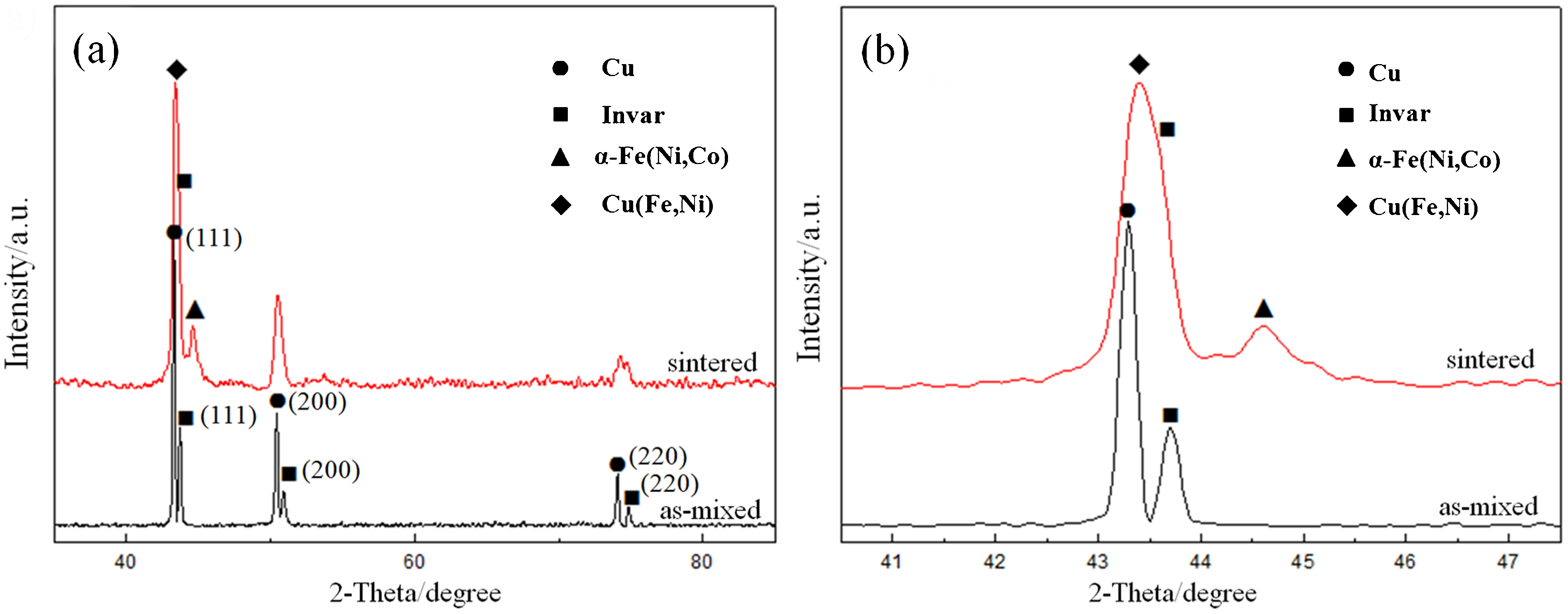
Patterns (XRD) of Cu/Invar composites a after mixed and sintered (sample A1B1C1D1); b magnified region of a close to reflection angle 2
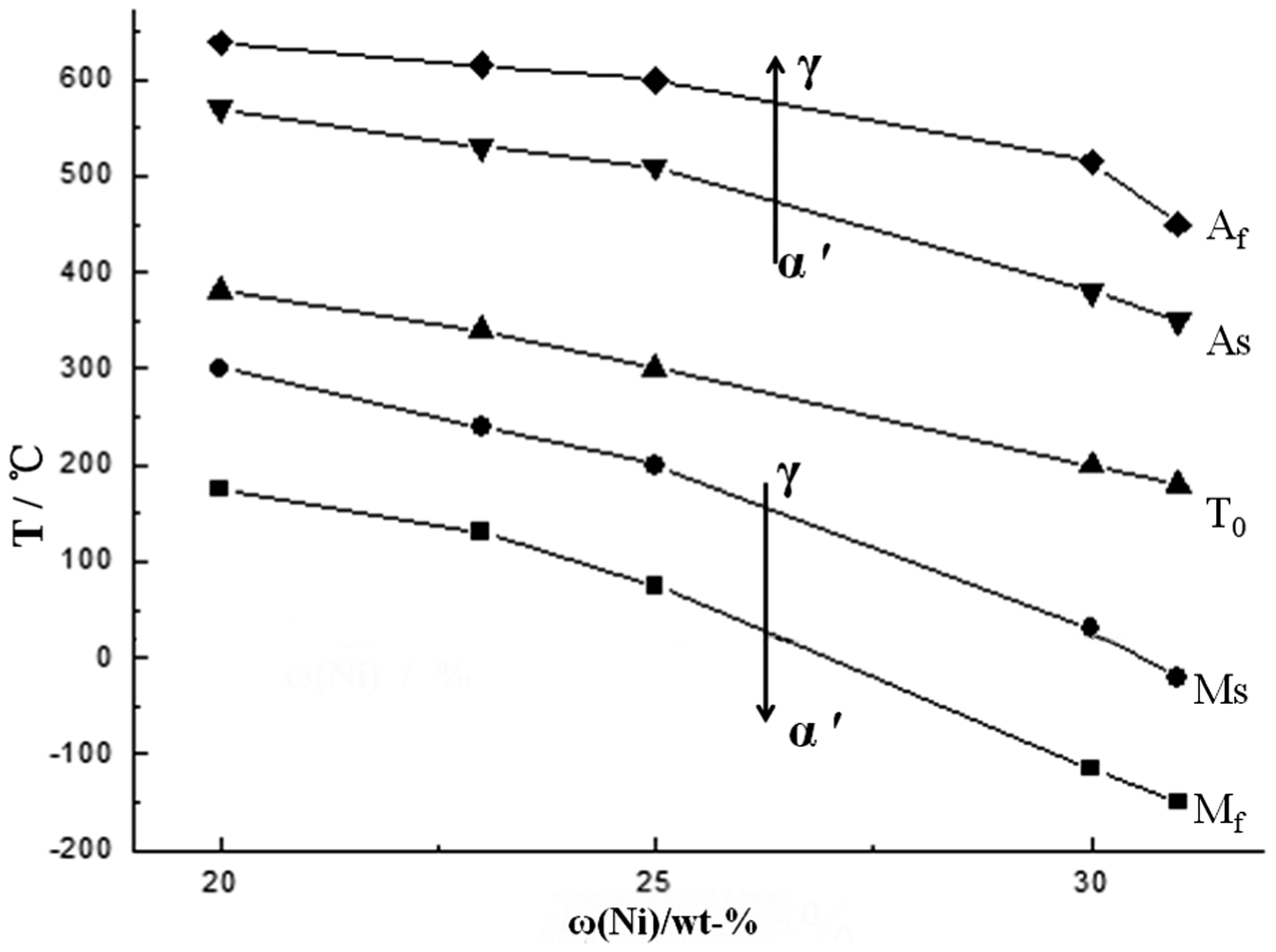
Effects of Ni content on Ms, Mf, As and Af points of the Fe–Ni alloy
Results of lattice parameters of phases in Cu/Invar composites
SEM and EDS analyses
In Fig. 3, two components are distributed uniformly in the composites, the dark region refers to the Invar powder, and the bright region refers to the Cu matrix. Owing to the lower hardness and higher ductility of Cu than the Invar alloy, the Cu particles are easily deformed and filled into the interspaces of the Invar particles in the forming process, which is beneficial to densification of the Cu/Invar composites. Cu distributes discontinuously in the Cu/Invar composites of 30 wt-%Cu. The Cu component is isolated by the continuously-distributed Invar component (Fig. 3a). As for the Cu/Invar composites of 40 wt-%Cu and above, the Cu component constructs a continuous net structure, meanwhile, the Invar particles distributes discontinuously in the Cu matrix (Fig. 3b and c). Moreover, several holes existed and preferentially distributed in the Invar particles. It is because that the sintering temperature of the composites (near 1100°C) is not high enough to make the Invar alloy powder densify fully, owing to the higher melting point of the Invar alloy (about 1450°C).
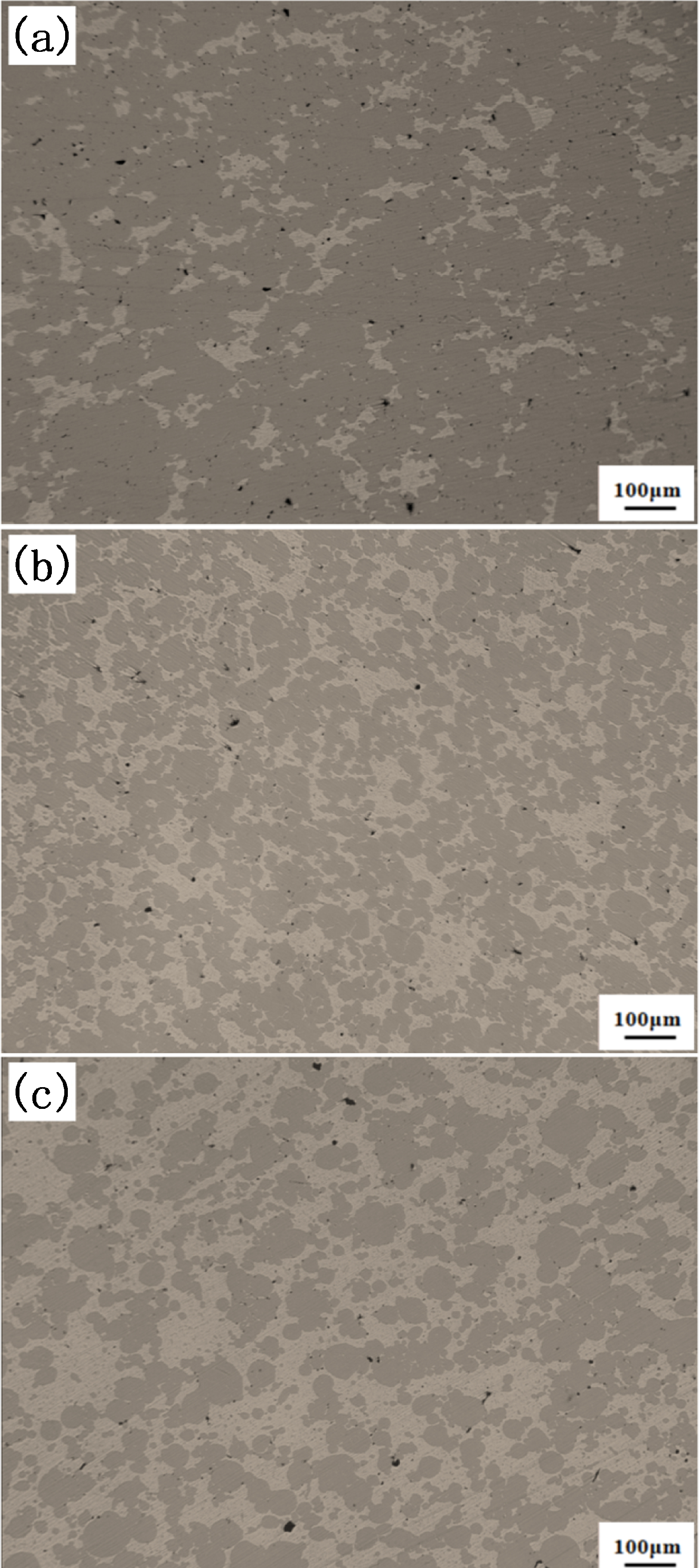
a A2B2C3D1; b A2B3C1D2; c A3B2C1D3
Microstructures, especially the distribution of Cu in the Cu/Invar composites, have great effects on the electrical and thermal conductivities of the composites. As mentioned above, when the Cu content in the composites is more than 40 wt-%, a continuous Cu net structure forms. Because the electrical resistivity of Cu is as low as 1.7 μΩ cm, 6 free electrons can migrate fluently through the continuous Cu conductor net in the process of the electrical resistivity test of the Cu/Invar composites. On the contrary, When the Cu content is lower than 30 wt-%, the Invar component is continuous, and Cu isolates in the Invar matrix. The Invar alloy has a much higher electrical resistivity of 83.3 μΩ cm, 17 free electrons have to transmit across the high-resistivity Invar component in the process of the electrical resistivity test of the Cu/Invar composites. That is the reason why the electrical and thermal conductivities of the composites are sensitive to the Cu content of the Cu/Invar composites.
Besides the microstructures, the compositions also have great influences on the electrical conductivities of the Cu/Invar composites. Based on the EDS analysing results (Fig. 4b–e), the Cu/Invar interface is located at 50 μm away from the O point in Fig. 4a, the left region is the Invar alloy and the right region is Cu. The Cu atoms almost diffuse throughout the whole Invar region, and the Cu content along the Invar grain boundaries is higher (Fig. 4b). Similarly, the Fe and Ni atoms also significantly diffuse into the Cu region (Fig. 4c and d). The intensities of the Fe and Ni element spectra in Cu are nearly equal to each other, but much higher than that of the Co element spectrum. Therefore, the diffusion of Fe, Ni results in the decrease in the Fe, Ni contents, especially the Ni content in the Invar alloy, and the formation of α-Fe (Ni, Co). In Fig. 4a, the composition of the Invar alloy (point A) and that of Cu (point B) across the Cu/Invar interface were measured. The Cu content in the Invar alloy (point A) is 10.84 wt-%, and the Fe, Ni contents in Cu (point B) are 7.14 and 6.82 wt-%, respectively. The Fe content in Cu has an abominably effect on the conductivity of Cu. When the Fe content in Cu is 5 wt-%, the electrical resistivity increases more than 5 times from 1.7 μΩ cm of pure Cu to 10 μΩ cm of the Cu–Fe alloy. 18 Correspondingly, the thermal conductivity of Cu also sharply decreases, due to the dissolution of Fe in Cu. As shown in Fig. 1, the decrease in the Ni content in the Invar alloy causes the change of the crystal structure of the alloy, and thus the CTE of the Invar alloy increases. In summary, in order to obtain high-quality Cu/Invar composites with high mechanical properties, electrical and thermal conductivities and low CTE, the atom diffusion inhibition of the Cu/Invar composites during sintering is necessary. In the subsequent research, the authors plan to solve the problem via the innovative methods, e.g. installation of a diffusion barrier at the Cu/Invar interface and alloying of Cu.
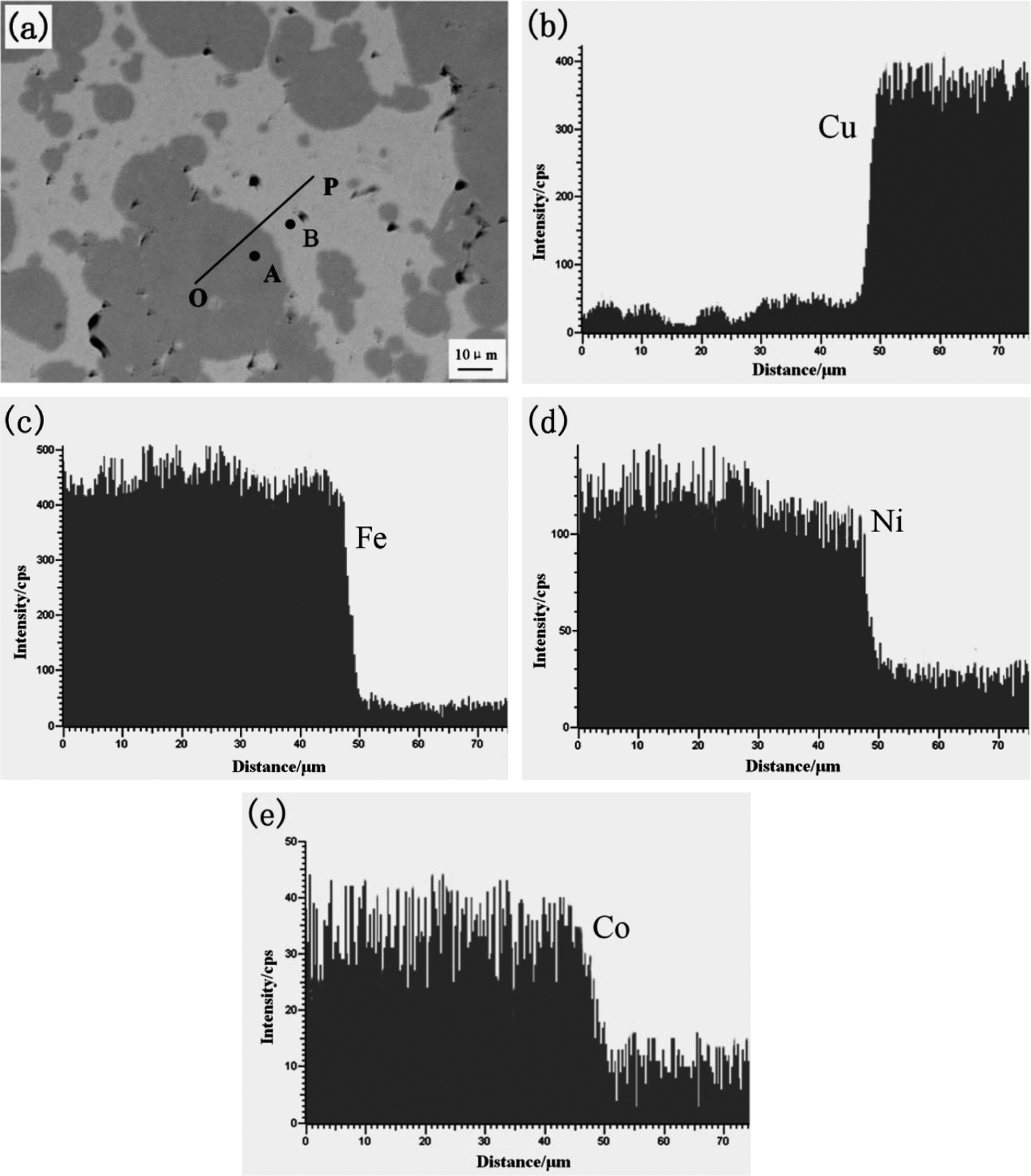
a SEM image; b–e linear scanning spectra of Cu, Fe, Ni and Co elements along OP line in a
Conclusions
The optimal PM processing parameters of the Cu/Invar composites were obtained, taking hardness and electrical resistivity as indexes, respectively. Taking the hardness as index, the optimal processing parameters are: forming pressure of 600 MPa, sintering temperature of 1150°C, holding time of 90 min and Cu content of 50 wt-%. Taking the electrical resistivity as index, the optimum processing parameters are: forming pressure of 600 MPa, sintering temperature of 1000°C, holding time of 60 min and Cu content of 50 wt-%.
During sintering the Cu/Invar composites, the Fe, Ni atoms in the Invar alloy diffuse into Cu to form the Cu (Fe, Ni) solid solution. Meanwhile, the Invar alloy partly transforms from γ-Fe (Ni, Co) phase of the fcc structure to α-Fe (Ni, Co) of the bcc structure due to that the Ni content reduces to 30 wt-% and below in the Invar alloy.
Microstructures of the sintered Cu/Invar composites vary with the compositions of the composites. When the Cu content of the composites is 30 wt-% and below, the Invar alloy is the continuous matrix in which Cu distributes discontinuously. When the Cu content is 40 wt-% and above, a net structure of Cu constructs in which the Invar alloy particles distributes discontinuously. Low density and the atom interdiffusion in the Cu/Invar composites are two key issues that have great effects on the properties, especially the electrical and thermal conductivities of the composites.