
Abstract
A bias voltage apparatus is attached to the filtered cathode vacuum arc system for coating a diamond-like film containing Ti on WC substrate. Ti, which acts as the cathode target, is sputtered by plasma, and reacts with C2H2 gas, then deposits on the WC under working conditions of 60 A current and voltage between −50 and −275 V. Such processed diamond-like film containing Ti(Ti–C:H) is analysed by glow discharge spectroscopy, X-ray diffraction, X-ray photoelectron spectroscopy and nanoindentation for determining Ti concentration, crystallographic structure, bonding mode and mechanical properties. Characteristic parameters are determined to obtain suitable properties, and the underlying reasons are also addressed.
Introduction
Diamond-like carbon (DLC) films have attracted considerable attention for their properties of hardness, optical transparency, low coefficient of friction, chemical inertness and high electrical resistivity. These properties are useful for a wide range of applications, including low friction and wear resistant coatings, protective optical and biomedical coatings, electroluminescent materials and field emission devices.1 – 5 High residual stresses in films result in poor adhesion of the growing DLC film, and this constrains the film thickness and limits the potential scope of application.6 Recently, researchers have reported reduction in internal stresses by doping the films with additional elements, such as Ti, Cr, Zr, W, Al, Cu and Fe.7 – 10 Methods for incorporating these metals into the DLC matrix include sputter deposition,11,12 plasma enhanced chemical vapour deposition13,14 and ion beam assisted deposition.15,16 Among the methods for the preparation of metal containing DLC films, the filtered cathode vacuum arc (FCVA) process is particularly useful for industrial application, because it provides fully ionised plasma of energetic ions for the bombardment on the substrate, which in turn, improves adhesion between adjacent films and substrates. Filtered cathode vacuum arc system can effectively filter out undesired particles by controlling the magnetic field in the plasma transportation duct to overcome the drawbacks of cathodic arc evaporation deposited DLC films.17 The kinetic energy of these ions which through the plasma transportation duct can be precisely controlled by adjusting the bias voltage applied to the substrate, so the influence of kinetic energy of ions on the structure of Ti doped DLC films. No literature on investigations into surface roughness, or other properties of Ti–C:H films fabricated using FCVA can be found. We used DLC film fabricated using the FCVA method, as a catalyst for Ti plasma, to synthesise Ti–C:H films using FCVA deposition with a negative bias voltage, in the presence of ethylene and argon gas. The FCVA technique, which is free of macroparticle contamination, is an effective method for depositing high quality nanocomposite films. The current study investigates the effects of a negative bias voltage on the nanostructural and mechanical characteristics of Ti–C:H films.
Experimental
Ti–C:H film was deposited onto a tungsten carbide (WC–Co) and SUS304 substrate using filtered cathodic arc deposition in a single step (Fig. 1). The carbon and titanium plasmas were produced in vacuum from an arc spot on a cathode target of 50 mm diameter. Carbon and titanium plasmas were produced under vacuum from an arc spot on a cathode target, 40 mm in diameter. The titanium target had a purity of 99·8%. The deposition system base pressure was 8·5×10−6 Pa. A curvilinear axial magnetic field was introduced to the system via an off-plane, 90° bend curved toroidal duct. The plasma was steered by the field through a duct into the deposition chamber. The plasma ions were deposited on the substrate without macroparticle or neutral atom contamination. The dimension of the substrate wafer was 10×10×3 mm and surface roughness was 0·05 Ra. All samples were cleaned ultrasonically in an acetone bath for 20 min, dried in a stream of nitrogen gas, and loaded into a substrate holder. Before deposition, the chamber was evacuated to 8·5×10−6 Pa. The substrate samples were subjected to glow cleaning for 30 min with addition of Ar at a pulse bias of −600 V and a pressure of 3·5×10−3 Pa. After substrate cleaning was finished, the deposition process commenced. Argon gas was supplied at a flowrate of 13 sccm, and a steady arc was maintained at a current of 60 A and under a deposition pressure of 1·0×10−4 Pa. Substrate, pulsed biasing was performed at 350 kHz pulse frequency, at a negative voltage with a duty cycle of 60%. The deposition procedure involved three steps. First, the substrate surface was bombarded with Ti cation for 1 min at 600 V negative bias. Second, pure 0·2 μm thick Ti film was deposited onto the substrate at −100 V for 5 min. Finally, for the formation of Ti–C:H films, acetylene (C2H2) was gradually introduced into the chamber using a mass flow controller. The Ti–C:H films were deposited with varying substrate bias voltage ranging from −50 to −275 V for 50 min. Table 1 lists the deposition process parameters. The DLC films containing Ti were characterised using an X-ray diffractometer (XRD; BRUKER D8A, Germany, Cu Kα radiation, 20–80°), a glow discharge spectrometer (GDS; LECO GDS-750QDP) and an X-ray photoelectron spectrometer (XPS; Thermo VG-Scientific, England). The hardness and Young's modulus of the films were investigated using nanoindentation techniques (MTS Nanoindenter XP).18 The indenter was operated in a constant displacement rate mode, and three indents were made per film.
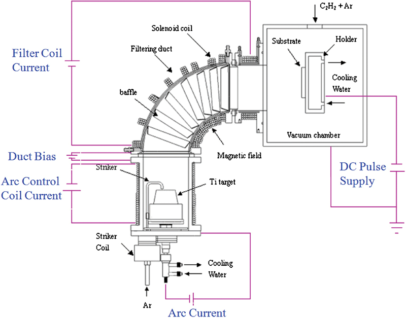
Schematic of apparatus for measuring FCVA systems
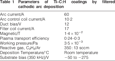
Parameters of Ti–C:H coatings by filtered cathodic arc deposition
Results and discussion
Film layer analysis by GDS and XRD
Figure 2 shows the DLC film (Ti–C:H) containing Ti formed with a target current of 60 A and voltage bias of −150 V. The percentage and depth of the C, Ti and W atoms were analysed using GDS. The film deposition structure, or matrix, consisted of a Ti interface layer, a TiC gradient layer and a Ti–C:H layer. The purpose of the Ti interface was to improve adhesion between the substrate and DLC film. Ti atoms in the gradient layer gradually decreased in concentration with proximity to the gradient layer and Ti–C:H layer boundary, to that of the Ti–C:H film. Figure 2 shows that the Ti interface layer was ∼0·1 μm thick, while the gradient layer and Ti–C:H layer were about 0·1 and 1·5 μm thick respectively. From the figure, the percentage of titanium atoms in the Ti–C:H layer was ∼11%. Figure 3 shows the X-ray diffraction curves of three sample test pieces which were SUS304 substrate, the Ti substrate, the Ti interface layer, and the Ti–C:H layer, from the bottom to the top. The Ti interface layer exhibited Ti (100) crystal peaks at 35° diffraction angle. This occurred because titanium cations migrated from the bombarded surface under the negative voltage bias. The kinetic energy of the ions converted to heat energy upon impact with the surface, and Ti crystallisation occurred on cooling as the material migrated away from the impact site. The amorphous structure seen at the surface of the Ti–C:H layer in Fig. 3, supports this migration crystallisation mechanism.
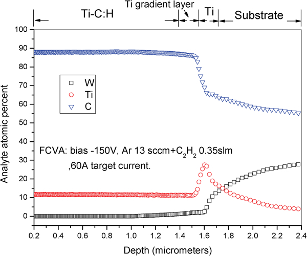
Quantitative GDS depth profile of efficient Ti–C:H coating
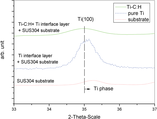
Ti–C:H film X-ray diffraction patterns
Titanium content and deposition rate
Figure 4 shows how the titanium content increases, following an S pattern as voltage bias increases. Ti content increases from 11% at −50 V to 12·94% at −270 V. This occurs because ion kinetic energy during bombardment increases with voltage bias, and Ti–C forms at higher bonding energies. The titanium atoms have larger mass than carbon atoms, so when Ti ions bombard the substrate surface, the smaller carbon atoms sputter more easily than titanium, or titanium carbide. Thus, the titanium content in the film increases with voltage bias. Figure 4 shows a relational curve describing that the deposition rate changes with the voltage bias; the deposition rate increases from 1·80 nm s−1 at a voltage bias of −50 V to a maximum of 1·93 nm s−1 at a voltage bias of −100 V. The deposition rate was reduced to 1·74 nm s−1 at a voltage bias of −150 V, and maintained at this level during further increases in the voltage bias. At higher voltages bias, the film was subjected to higher energy bombardment, and as the energy grew, anti-sputtering, or deposition atoms, migrated to the cathodic dark space. Consequently, the deposition rate is decreased as voltage bias increased, and the curve of the deposition rate was flat between −150 and −275 V.
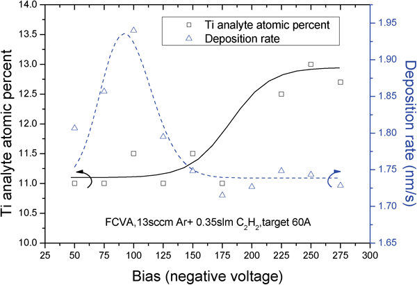
Relation of titanium content, deposition rate and voltage bias
XPS
Figure 5 shows the XPS C1s energy spectrum of a test sample of the titanium-containing DLC film formed with the voltage bias of −125 V. Before measuring, the sample was etched for 20 min to remove the oxide layer formed on exposure to air. The C1s energy spectrum is an asymmetrical curve. We resolved the energy spectrum through Gaussian shape to reveal combinational waveforms of sp3 and sp2 bonding, and peaks appear at 285·4 and 284·5 eV respectively.19 The sp3 hybridisation describes tetrahedral, diamond type bonding, and sp2 represents planar graphite structural bonding. The area below the waveform curve represents the relative contents of the sp3 and sp2 bonding modes present in the carbon film. Figure 6 represents the change in the sp3/sp2 hybridisation ratio with increasing voltage bias. The single-crested curve peaks at a ratio of 0·52, at a voltage bias of −100 V, in agreement with previous reports.20 Carbon ion sp3 bonding requires an ionic energy of 100 eV. If an ion energy greater than 100 eV bombards the surface, it penetrates into the sublevel and produces heat. Heat in turn provides extra energy and the sp3 bonding mode converts to sp2 hybridisation. Thus, the sp3 content is a key factor in the hardness, elasticity modulus, wear, surface roughness, and other physical properties of the carbon film, and is an index type parameter. In Fig. 6, the amount of sp3 bonding was at a maximum when the voltage bias was −100 V. The sp3/sp2 ratio decreased as voltage bias increased further. Therefore, titanium-containing DLC film becomes more graphite-like at voltage bias values greater than −100 V. In Fig. 7, the Ti2p1 and Ti2p3/2 peaks appear at 461·2 and 455 eV respectively, and represent Ti–C carbide bonding.20 We used FCVA titanium plasma-source ionised C–H reaction gas for the deposition of the Ti–C:H film. The titanium transferred from the target formed Ti–C carbide material, which deposited onto the film surface.
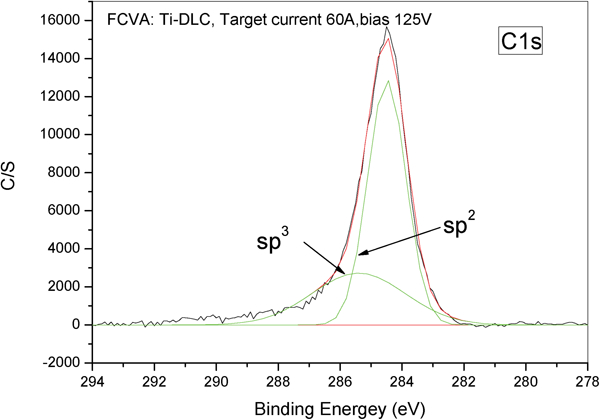
C1s energy spectrum of test piece of titanium containing DLC film for voltage bias of −125 V, as measured by XPS
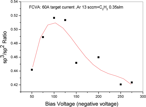
Relation between voltage bias (−50 to −275 V) and sp3/sp2 ratio
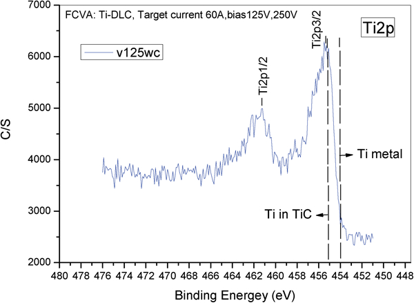
Ti2p energy spectrum
Nanoindenter
Figure 8 shows the variation in hardness and depth with voltage bias. The hardness and Young's coefficient of the film samples were determined by a Berkovich three-sided taper diamond probe of the nanoindenter. The data presented for each curve in Fig. 8 are the average of 16 separate measurements. Hardness and Young's coefficient were measured at 1/10 of the film thickness. Figure 9 shows a single-crested hardness curve for voltage bias varying from −50 to −275 V. Hardness varies from 12 GPa to a maximum of 18·3 GPa. The maximum hardness value occurred for a voltage bias of −175 V. As bombardment energy increased with the voltage bias, the deposited atoms acquired sufficient kinetic energy to migrate penetrated to vacant sites. Therefore, more efficient packing increased film density, hardness, Young's modulus and residual stress.16 The hydrogen atoms in the C–H gas were added to the structure during deposition of the carbon film. Although the hydrogen atoms stabilised sp3 bonding in the structure, they decreased the carbon film stability. When the voltage bias increased, the increase in bombardment energy provided sufficient kinetic energy for incoming ions to break the C–H bonds. The Ti ions displaced the hydrogen atoms, and formed bonds with the carbon atoms to form stable Ti–C carbide bonds. Moreover, under high energy bombardment, degree of cross-linking within the film increased, making the film structure denser and improving hardness. Titanium added substrate altered the carbon film structure. Consequently, the maximum hardness seen in the plot of Young's modulus versus voltage bias (Fig. 9) occurred at a voltage bias of −175 V, instead of the value of −100 V, which produced the greatest sp3 content. When voltage bias exceeded −175 V, ion kinetic energy converted to heat energy. As the temperature increased, conversion of sp3 bonding into sp2 bonds resulted in a decrease in hardness. The addition of titanium stabilised sp3 bonding, though some C ions formed into sp2 bonding at lower free energy levels. This is why the hardness curve in Fig. 9 indicates that the hardness decreased when the voltage bias exceeded −175 V. In Fig. 9, Young's modulus lies between 120 and 180 GPa. Young's modulus was greatest (180 GPa), at a voltage bias of −175 V and lowest (120 GPa) at a voltage bias of −50 V. Young's modulus relates to material stress, strain and chemical composition. A high value for Young's modulus implies higher bonding energy between atoms, a longer bonding distance between atoms, and higher ionic content and metallic bonding.
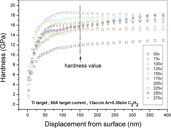
Relation between hardness and depth under different voltage bias
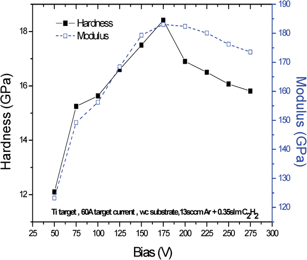
Relation of hardness, Young's modulus, and voltage bias parameter
Conclusion
Applying bias voltage in FCVA process for coating diamond-like film containing Ti on WC substrate is effective in modifying properties of hardness and Young's modulus. Two characteristic bias voltage, −100 and −175 V, are determined which can yield optimal properties. For the −100 V, film deposition thickness reaches a maximum of 1·93 mm s−1, while the highest hardness and Young's modulus are obtained at −175 V. This can be attributed to the fact that Ti–C forms and steadily deposits on the substrate. Hence, coating with a film of diamond like structure can give tribological advantage, as it lowers friction coefficient, reduces wearing rate and resists corrosion.