
Abstract
This study mainly aims to evaluate the intermixing between layers during the deposition of dielectric/metal/dielectric nanoscale multilayer coatings. TiO2 and WO3 films as dielectric materials are developed using radio frequency reactive magnetron sputtering on unheated soda lime glass substrates. Ag films are grown using radio frequency argon sputtering. Auger electron spectroscopy and ultraviolet–visible–near infrared spectrometry are employed to estimate the degree of layer intermixing in TiO2/Ag, WO3/Ag, TiO2/Ag/TiO2 and WO3/Ag/WO3 films. The morphological properties are also investigated under a field emission scanning electron microscope and an atomic force microscope. The transmittance curves for bilayer films exhibited heat mirror effects significantly. However, multilayer films showed a little amount of heat mirror effects. Auger electron spectroscopy depth profiles confirmed a minor diffusion of Ag at the TiO2/Ag interface. However, significant interactions of WO3 with Ag were observed for the WO3/Ag film. Besides, severe intermixing and oxidation of Ag films were observed for the multilayer films.
Introduction
TiO2 is a very popular material for many optical applications because of its high refractive index, transparency in the visible region, high stability against adverse environment and mechanical hardness. The demand for optical coatings on a large area has been increasing, e.g. the heat cutting window coatings such as low emissivity coatings and the antireflective coatings for architectural and automobile windows.1 – 4 WO3 is one of the most widely studied electrochromic materials used as films.5 A promising application for these coatings is a switchable glazing for a smart window, which can save energy for air conditioning. Recently, WO3 films have been considered for use as dielectric layers in dielectric/metal/dielectric (DMD) multilayer heat mirror coatings on building and automotive glasses. 1 4 1,4,6 Dielectric/metal/dielectric transparent electrodes based on WO3/Ag/WO3 have applications as cathodes for displays based on organic light emitting diodes.7 Most of the applications using DMD multilayer structures are transparent heat mirror coatings for economical and ecological windows. The optical requirements of the heat mirror are a high transmittance in visible light and a high reflectance in infrared light.
It is commonly known that sputtering is the most suitable means for these kinds of large area coatings because it gives a high uniformity of thickness and film quality. The sputter deposition technique is also popular to produce adherent film over wide areas with better stoichiometric control. Therefore, sputtering is becoming the mainstream in large area optical coating methods.
In multilayer coatings, the properties of the interface and the extent of the components at the interface are important questions both for the applications and from fundamental point of views. Most of the works 1 2 4 6 1,2,4,6,7 deposited dielectric layers using either thermal evaporation or electron beam evaporation for the development of DMD structures. In those works, very little intermixing of layers was reported. Tachibana et al.3 also reported dc sputtered TiO2/Ag/TiO2 films without any intermixing. In that work, TiO2 was deposited using the ceramic targets, and oxygen deficient TiO2−x and the mixed gases of a few per cent of O2 diluted with Ar were used as sputter gas. Yamamoto et al.8 reported the chemical state of the ZnO/Ag film interface using secondary ion mass spectrometry. In that work, ZnO/Ag/ZnO multilayer samples were deposited on soda lime glass substrates by dc sputtering. During the reactive sputtering of the top layer ZnO film, they observed oxidation of the Ag film with some intermixing.
In the present work, dielectric layers of DMD multilayer structures were deposited by radio frequency (rf) reactive magnetron sputtering of metallic targets (titanium and tungsten). The interface properties of DMD structures have been investigated using Auger electron spectrometry (AES) and ultraviolet–visible–near infrared spectroscopy. The morphological properties of different films are also investigated under a field emission scanning electron microscope (FESEM).
Experimental
Single, bilayer and multilayer films of TiO2, WO3 and Ag were deposited on microscope glass slides at room temperature using a dual target dc/rf magnetron sputtering system with a rotatable substrate holder. The oxide films were prepared by rf reactive sputtering from metallic targets, and the Ag films were deposited using rf around plasma only. The summarised values of the different deposition parameters are given in Table 1. Before the deposition of single or first layer, the respective target was presputtered for 10 min in an argon atmosphere to remove the oxide layers. The sputtering chamber was evacuated down to 5×10⁻⁴ Pa by a turbomolecular pump. Before the deposition, the glass slides were sequentially cleaned in an ultrasonic bath with acetone and ethanol. Finally, they were rinsed with deionised water and dried with the blow of dry nitrogen (99·999% purity). During the deposition of multilayer thin films, the substrate temperature rises slightly from 20 to 35°C.
Summary of parameters for TiO2, WO3 and Ag films deposited on microscope glass slides at room temperature
The phases present in the single layer films were analysed by an X-ray diffractometer (model D5000, Siemens) using Cu Kα radiations (λ = 0·15406 nm) and operating at an accelerating voltage of 40 kV and an emission current of 40 mA. The transmission spectra of different films were measured using a Jasco V-570 (USA) double beam spectrophotometer. The transmission measurements were performed at room temperature and normal incidence in the wavelength region of 250–2500 nm at a bandwidth of 2 nm.
The surface morphology of the different films was characterised using FESEM (FEI Quanta 200 FEG-SEM). The thicknesses of single layer films were measured under SEM as well. Auger electron spectroscopy depth profiling of different bilayers and multilayers was performed using a JEOL JAMP 9500F field emission scanning Auger microprobe. The depth profiling for different samples was performed with the electron gun set at 2 keV at an incidence angle of 30° with respect to the surface normal. For surface morphology, atomic force microscopy (AFM) images were recorded using a Nanoscope IIIa scanning probe in tapping mode. The cantilever oscillates at a frequency of ∼285·0 kHz and operates at a scan rate of 1 Hz in the atmospheric conditions. The surface morphology and the root mean square (RMS) surface roughness values were obtained from regions of 500×500 nm for titanium oxide films.
Results and discussion
Structural and optical properties
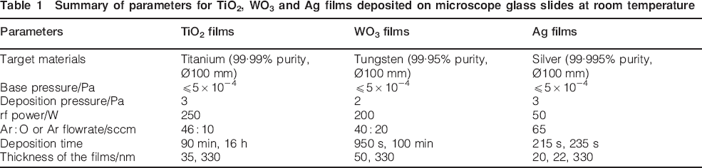
To evaluate structures using the X-ray diffraction method, single layer TiO2, WO3 and Ag films of similar thicknesses (∼330 nm) were used. The diffraction patterns of the different single layer films are shown in Fig. 1. The as deposited TiO2 film at room temperature was found to be crystalline and possessed an anatase structure as it shows few strong peaks of anatase (101), (200) and (211) planes. On the other hand, the WO3 film deposited at room temperature was observed to be amorphous. Furthermore, the single layer Ag film was found to be polycrystalline, having a cubic structure in the present work. It was observed from the literature that a wide variety of structures can be obtained in sputter deposited TiO2 films depending on the deposition conditions. On unheated substrates, amorphous, 9 9,10 anatase, 11 11,12 rutile13 and a mixture of anatase/brookite14 titanium oxide films were obtained by different researchers. Liu et al.11 and Sung and Kim12 observed anatase phase in their sputtered TiO2 films deposited at a pressure of 1 Pa or above. At high pressure, the depositing species have lower energy; there are suggestions that high density negative oxygen ions have high mobility at high pressure, which impart high energy to the growing film.10 This may be the reason for the growth of the crystalline anatase phase in the present study at low temperature and high deposition pressure (3 Pa). However, the tungsten oxide films were found to be amorphous deposited at different pressures from 1·5 to 5·2 Pa using dc reactive magnetron sputtering.15 It may be attributed to the lower energy of the heavier tungsten oxide species deposited at higher pressures. For a high Ar pressure of 5 Pa, the polycrystallinity observed for Ag films prepared by rf magnetron sputtering at room temperature is comparable to that of the present study.16
X-ray diffraction spectra of WO3, TiO2 and Ag films of similar thickness (∼330 nm) deposited on microscope slides
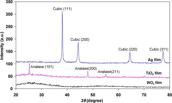
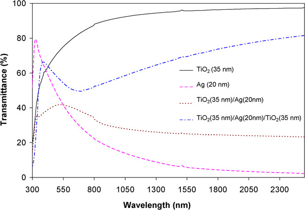
Considering Ag film of 20 nm thickness, TiO2/Ag/TiO2 and TiO2/Ag were developed and are shown in Fig. 2. The figure also shows the transmittance curves of thin titanium oxide (35 nm) and silver film (20 nm). It is observed that the thin titanium oxide film shows high transmission of light in the visible and infrared regions. The Ag film shows very low transmittance in the infrared region. The TiO2/Ag film is seen to have visible transmittance of ∼40% and low infrared transmittance (∼25% at 2500 nm) compared to the triple layer structure. However, the triple layer film of TiO2/Ag/TiO2 exhibits high transmittance at both visible and infrared regions. Figure 3 shows the variation of transmittance curves for thin WO3 film (50 nm thick), WO3 (50 nm)/Ag (22 nm) film and WO3 (50 nm)/Ag (22 nm)/WO3 (50 nm). The double layer film (WO3/Ag) distinctly shows low transmittance to infrared light and comparatively higher transmittance of visible light (∼40%). The low infrared transmittance of the TiO2/Ag film indicates a limited heat mirror effect. On the other hand, TiO2/Ag/TiO2 film having high infrared transmittance is considered as a DMD film without any heat mirror effects. From the literature, several reports are found to investigate the optical behaviour of TiO2/Ag/TiO2 films deposited on glass substrates at a comparable thickness to the present work. A summary of previous works is given in Table 2. Several works 1 2 1,2,4 developed inner and outer TiO2 layers using ceramic targets of TiO2 by electron beam evaporation. The middle Ag films were prepared by thermal evaporation. All those works reported high visible and very low transmittances at infrared range. Tachibana et al.3 observed moderate visible transmittance (68%) for the five-layer stacks of TiO2 and Ag. In that work, the TiO2 films were deposited by dc magnetron sputtering of ceramic target (TiO2−x) at an argon and oxygen atmosphere, where the oxygen content is only 3% of the total mixture. In the present work, titanium oxide films were deposited by rf reactive magnetron sputtering of titanium target using a higher content of oxygen.
Transmittance curves of single and multilayer films of TiO2 and Ag
Transmittance curves of different single and multilayer films of WO3 and Ag
Results of previous works for TiO2 based multilayer films*
TVis: average visible transmittance; TIR: transmittance at 2500 nm wavelength.
On the other hand, the behaviour of single and multilayer films of WO3 and Ag is observed to be nearly comparable to that of TiO2 and Ag films, as discussed earlier. In both cases, the DMD multilayer structures did not fulfil the optical requirements of transparent heat mirror coatings. Very few works 1 4 1,4,7 are found to investigate WO3/Ag/WO3 films for window glazings. In those works, WO3 films at a thickness of 35–40 nm by thermal evaporation exhibited low transmittance at infrared range for the multilayer stacks. Bertran et al.17 prepared DMD multilayer structures by rf magnetron sputtering of dielectric targets [indium tin oxide (ITO)]. In that work, ITO and Ag were deposited on glass at a thickness of 50–100 and 3–10 nm respectively. Most of the ITO/Ag/ITO films did not show heat mirror effects having a high infrared transmittance. In that work, the lower thickness of Ag might be the reason for this. Therefore, it can be thought that the high transmittance of infrared light of the studied triple layer structures may be ascribed to the reactive magnetron sputtering at higher oxygen content and other deposition parameters used.
Auger electron spectroscopy analysis
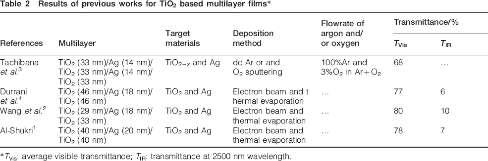
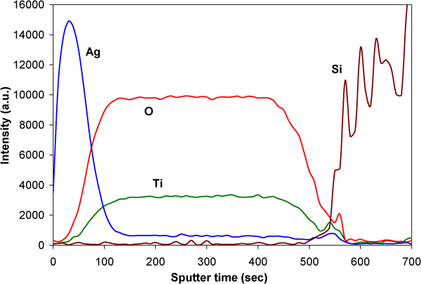
Auger electron spectroscopy depth profiles of TiO2/Ag film, as shown in Fig. 4, exhibit the quality of interface between silver and titanium oxide films. It is observed that two layers of Ag and TiO2 are easily distinguishable. Some intermixing of different elements in the narrow region of the interface might have happened. However, the two layers of Ag and TiO2 films are easily distinguishable. This supports the lower transmittance obtained in the infrared region of light, which indicates better heat mirror effects of the TiO2/Ag film (Fig. 2). The AES depth profiles for the TiO2/Ag/TiO2 film were also investigated to see the elemental distribution of the multilayer (Fig. 5). From Fig. 5, it is observed that there is a strong intermixing of the different elements, which practically results in a single layer structure having titanium and oxygen at a uniform proportion. Ag is observed to be diffused into both inner and outer TiO2 films. It is thought to be a joining of the inner and outer TiO2 films and the diffusion of Ag film into these films. As a result, the transmittance curve of the TiO2/Ag/TiO2 film behaves like a single layer film that shows a single interference fringe in the spectrum (Fig. 2).
Auger electron spectroscopy depth profile of TiO2/Ag film deposited on glass substrate
Auger electron spectroscopy depth profile of TiO2/Ag/TiO2 film deposited on glass substrate
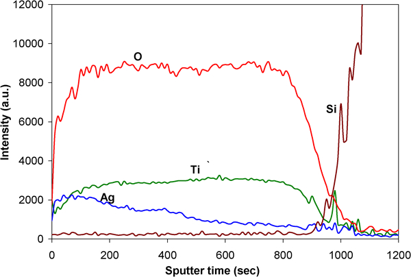
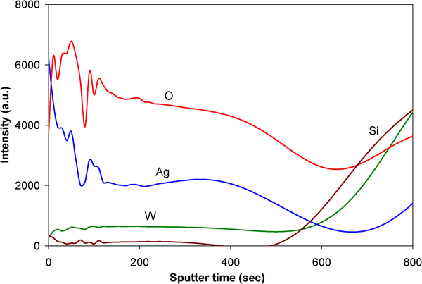
Figure 6 shows the depth profiles for WO3/Ag film. From the depth profiles of different elements, it is observed that the outer film of silver is partly intact. For the distinct formation of WO3, it is necessary to find the O and W peaks together. In this case, the O peak moves towards the Ag peak, which indicates higher interactions among the Ag and O species. It also seems that the oxygen species diffused into the Ag film to produce silver oxide with some intermixing of Ag and WO3 films in the interfacial region. From Fig. 6, it is observed that the oxygen peak overlaps with the silver peak, and the tungsten peak does not coincide with the oxygen peak. It may be thought that tungsten oxide decomposes partially into understoichiometric tungsten oxide and silver oxide forms in the interface. Pergament and Stefanovich18 reported that standard Gibbs free energy of formation for TiO2 and WO3 are 889 and 764 kJ mol−1 respectively. Therefore, the lower value of Gibbs free energy of formation for WO3 makes it more unstable than TiO2. The reaction of reduction proceeds preferentially, which causes more oxygen–silver interactions. The depth profiles of different elements for the WO3/Ag/WO3 films using AES are shown in Fig. 7. Elemental distribution, as shown in the figure, matches with the similar trend observed for the TiO2/Ag/TiO2 film. From Fig. 7, a strong intermixing of the different elements is observed, which results in a single layer structure having tungsten and oxygen at a uniform proportion. Silver is also observed to be diffused into both inner and outer WO3 films. However, it is found to migrate more into the outer layer of tungsten oxide.
Auger electron spectroscopy depth profiles of different elements in WO3/Ag film deposited on glass substrate
Auger electron spectroscopy depth profiles of different elements in WO3/Ag/WO3 film deposited on glass substrate
For both DMD structures using TiO2 and WO3, triple layer systems exhibit higher visible transmittance than bilayer systems, as mentioned earlier. From the AES results, it may be attributed to the formation of a single composite layer of titania–silver–silver oxide instead of the triple layer structures. It was reported by Al-Kuhaili et al.6 that the depth profiles of different elements showed different distinct layers with a slight intermixing for WO3/Ag/WO3 films prepared by thermal evaporation, and their films exhibited heat mirror effects with moderate visible transmittance and infrared reflectance. Tachibana et al.19 reported the preparation of Ag/TiO2 multilayer films on glass substrates using reactive sputtering of TiO2−x target. They observed a damage of oxygen on silver layers. The O species are implanted into the Ag film. The possible O species making damage on the Ag films are the backscattered O species originating from the positive ions sputtering the target and the O− ions generated and accelerated around the sheath nearby the target. From a comparison between the backscattering probability of O species and the number population of O− ions, it can be thought that O− ions mainly cause the Ag damage. In the present work, the findings confirm the severe oxidation of Ag and merging of three different layers. It is also suggested that in the overlapping zone of O and Ag at the interface, Ag2O can be thought to form.7 As a result, the observed higher values of transmittance at infrared range ( Figure 2 Figs. 2 and 3) are due to the reactive sputtering of metallic targets, which cause oxygen damage for silver films.
Morphological properties
The morphological properties of different layer stacks have been investigated using FESEM. Figure 8 shows the surface morphology of thin TiO2, TiO2/Ag and TiO2/Ag/TiO2 films at low and high magnification under FESEM. At low magnification (×1000), the TiO2 and TiO2/Ag films are found to be flat with homogeneous morphology. However, the triple layer film (Fig. 8c) shows different surface areas (dark and bright). It indicates an inhomogeneous film formation for the TiO2/Ag/TiO2 film. The film growth of TiO2 on glass substrate and of Ag on TiO2 coated glass substrate is found to be uniform and free from any defects. Besides, the SEM images at high magnification for TiO2 and TiO2/Ag are found to be flat and homogeneous. The dark and bright areas of the TiO2/Ag/TiO2 film at high magnification show a completely different morphology. The dark area shows film growth defects having non-uniform and agglomeration of materials. The bright area shows agglomeration of particles with a large number of holes around the surface. Images (SEM) at high magnification indicate higher surface roughness for the TiO2/Ag/TiO2 film. The findings of AES analysis can also be supported by the morphology of the films. In the bilayer TiO2/Ag film, the morphology is quite flat, indicating insignificant intermixing, and micrographs of TiO2/Ag/TiO2 films also support higher intermixing of different layers.
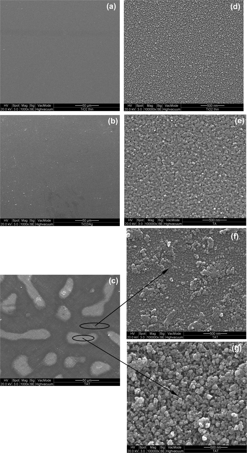
Images (FESEM) of a TiO2, b TiO2/Ag, c TiO2/Ag/TiO2 films at low magnification (×1000), d TiO2, e TiO2/Ag and f, g TiO2/Ag/TiO2 films at high magnification (×100 000)
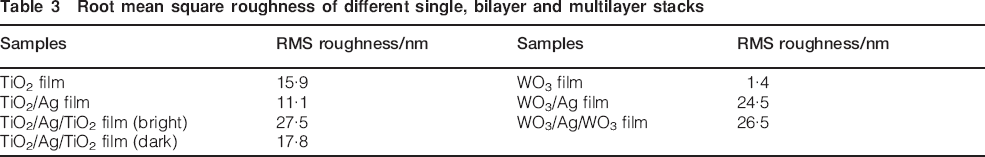
Figure 9 shows the different single, bilayer and multilayer thin films for tungsten oxide based coatings. From the figure, it is observed that the surfaces of the single and bilayer films are smoother than that of the multilayer structures. The surface roughness was assessed by AFM. Table 3 shows the RMS surface roughness of different samples. The surface roughness was almost unaffected by the formation of bilayer films for titanium oxide based multilayers. Al-Kuhaili et al.6 reported an RMS roughness of 1·66 nm for thin WO3 film (35 nm) prepared by thermal evaporation. In the present work, the RMS roughness for WO3 film (50 nm) is found to be 1·4 nm. TiO2/Ag/TiO2 and WO3/Ag/WO3 films being formed by densely narrow needles show a higher surface roughness. Therefore, it can be thought that the severe intermixing causes a high surface roughness. The AFM images (Fig. 9) confirm the intermixing and diffusion of different elements for both titanium and tungsten oxide based coatings. The higher surface roughness for triple layer structures is supposed to cause more scattering of light and consequently lower visible transmittance. Instead, the bilayer systems show lower visible transmittance because of the highly reflective upper silver film.
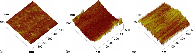
Images (AFM) of a WO3 film, b WO3/Ag film and c WO3/Ag/WO3 film
Root mean square roughness of different single, bilayer and multilayer stacks
Conclusion
Intermixing at the multilayer interfaces along with the morphological properties has been investigated for rf sputtered TiO2 and WO3 based coatings. Both TiO2/Ag and WO3/Ag films exhibit some heat mirror effects, but neither of the multilayer films exhibits low infrared transmittance. Auger electron spectroscopy depth profiles for TiO2/Ag show that two layers coexist with some intermixing at the interface. In WO3/Ag films, O and Ag intermixes significantly, but two layers are still distinguishable. Auger electron spectroscopy results also reveal that there is a strong intermixing of the different elements in triple layer structures of TiO2/Ag/TiO2 and WO3/Ag/WO3 films. Scanning electron micrographs show flat and homogeneous surface for TiO2 and TiO2/Ag films. However, TiO2/Ag/TiO2 film exhibits agglomeration of particles and sporadic scales of materials on the surface, which supports the intermixing. Images (AFM) reveal that the surfaces of the single and bilayer films are smoother than that of the multilayer structures. Both TiO2/Ag/TiO2 and WO3/Ag/WO3 films being formed by densely narrow needles show the highest surface roughness.
Footnotes
Acknowledgements
The authors gratefully acknowledge the financial support given for this work by the Ministry of Science, Technology and Innovation Malaysia (MOSTI) under the ScienceFund by grant no. 13-02-03-3033 and the Institute of Research Management and Consultancy, University of Malaya (UM) by PPP fund project no. PS 380/2008C. The authors also pay thanks to Professor Dr M. Hamdi, Department of Engineering Design and Manufacturing, UM, for allowing the authors to use his vital research facilities.