
Abstract
ZrTiN hard coatings were deposited on WC/TiC/Co cemented carbide substrate by multi arc ion plating. During the depositing, the four most important parameters are target current, nitrogen flowrate, deposition temperature and negative substrate bias voltage. This paper presented a detailed analysis of the effect of these four depositing parameters on the microstructures and properties of ZrTiN thin films respectively. In addition, we also systematically investigated the microstructure, elemental composition, crystal orientation, lattice parameter, grain size, adhesive strength and microhardness of the films. X-ray diffraction analysis indicated that only the face centred cubic phase was formed in the films, but the crystal orientation varied with different deposition conditions. Microhardness and adhesive strength of the coatings were associated with elemental composition, crystal orientation and microstructures. The optimum films obtained possessed comprehensive mechanical properties with an adhesive strength of 84·1 N and a microhardness of 30·4 GPa and exhibited the strongest (111) preferred orientation.
Introduction
Along with the rapid development of high speed machining technology in the past decades, the cutting environments become more and more extreme. Better performances of cutting tools, such as high hardness, wear resistance, strength, toughness and heat resistance, are demanded. At the present time, the cutting tool materials used in high speed machining are mainly diamond, cubic boron nitride, ceramic, cermets, coated carbide, etc.1 Surface coating is an effective way to improve the durability of the tools. Chemical vapour deposition (CVD) and physical vapour deposition (PVD) techniques have made it possible to deposit thin films (a few micrometres) on the surface in a wide range of deposition conditions. 2 2,3 Originally, due to their excellent properties,4 NaCl type transition metal nitride hard coatings were widely used to increase the working life and productivity of cutting tools, such as TiN, CrN and ZrN.5 – 8
Recently, more and more complicated materials are being studied and used, such as multilayer coatings and ternary materials, including TiCN, TiAlN, TiZrN and TiCrN, which have higher hardness and better wear resistance than TiN and ZrN coatings9 – 11 because of the solid solution strengthening. It has been reported that TiZrN and TiAlN coatings have better wear resistance because of the oxide layers generated on the surface of the coatings.12 – 14 The radiuses of Ti and Zr atoms are 0·132 and 0·145 nm, with a discrepancy of 9·85%. In the periodic table of elements, Ti and Zr belong to the same IVB family, and they have the same crystal structure as hexagonal close packed lattice. In addition, TiN and ZrN are both face centred cubic lattice. Accordingly, the substitutional solid solution ZrTiN was stable. Although some research has been carried out on ZrTiN coatings,15 – 17 discussion on phase composition, microstructure and property changes with depositing parameters is limited and unilateral.
In the present study, multi arc ion plating PVD ZrTiN coatings are deposited on WC/TiC/Co (WC+15%TiC+6%Co) cemented carbide substrates using a multiple use ion plating equipment. Phase structure, surface and cross-section morphology, lattice parameter and mechanical properties are systematically investigated. There are several parameters that affect the properties of the coatings, such as target current, nitrogen flowrate, deposition temperature and negative substrate bias voltage. Respectively, we investigate the effect of each parameter on the properties of ZrTiN coatings with the other parameters fixed. The aim of this work is to systematically investigate the changing trend of phase composition, microstructures and mechanical properties of multicomponent ZrTiN coatings with depositing parameters. We will obtain applicable depositing parameters for ZrTiN coatings and then provide theoretical and practical basis for further industrial production.
Experimental
The substrate material employed for this study was WC/TiC/Co cemented carbide, and the dimension of the substrate was 16×16×4 mm. The properties of the substrate material are listed in Table 1. The surface of the substrate was mirror polished and then cleaned ultrasonically in ethanol and acetone progressively, each for 15 min. Before depositing, the substrate was dried for 15 min in a prevacuum dryer.
Properties of WC/TiC/Co cemented carbide
The deposition was carried out using a multiple use ion plating equipment. The ZrTiN coatings were produced by multi arc ion plating with two symmetrically arranged Ti and Zr targets (of 99·9% purity) in Ar+N2 at a pressure of 0·45 Pa. The plasma incidence was vertical on the substrate. The distance between the targets was ∼600 mm. The substrate was fixed on the sample holder, and the sample holder was between two targets. The sample holder revolved both around the vacuum chamber axis and its own. The revolution and rotation of the sample holder at the same time made the film composition relatively uniform.
While depositing, the mass flow controllers were used to regulate the gas flow. The reactive gas partial pressure was decided by adjusting the nitrogen gas flow before the Zr target poisoning. Before the deposition, the coating chamber was evacuated down to 7·0×10−3 Pa and heated up to a certain temperature. Then, the substrate was cleaned and heated by ion bombardment during 2 min with a negative bias voltage of 800 V. In order to improve the adhesive strength, it was common to incorporate a metal interlayer between the film and the substrate. Before the reactive deposition, a metal interlayer Ti was deposited for 1 min and then TiZr for 2 min. The basic depositing parameters are listed in Table 2.
Basic depositing parameters
The microstructures of the surface and cross-section were observed by a scanning electron microscope. The elemental composition of the film was obtained from an energy dispersive X-ray detector. The preferred orientations of ZrTiN coatings were studied by X-ray diffraction (XRD) using a D8 ADVANCE (Bruker AXS) diffractometer with Cu Kα radiation. The lattice parameters of the films were also calculated from the XRD patterns. The grain sizes were estimated using the Debye–Scherrer formula18 D = Kλ/(Bcos θ), in which λ is the wavelength of the incident X-rays, K is the Scherrer constant for which the value here was 0·89, θ is the diffraction angle (Bragg angle) and B is the full wave at half maximum. The Scherrer formula was an evaluation method, with an error of about 0·5–1 nm.19
The adhesive strength of the coating–substrate system was obtained using scratch test on the surface property tester MFT-3000 by moving a diamond penetrator along the specimen's surface with a gradually increasing load. The tests were taken with the following parameters: ending load of 100 N, load increase rate of 100 N min−1 and penetrator's travel length of 4 mm. Microhardness measurements were taken on an MH-6 microhardness tester at 0·25 N loads, with eliminating influence of the substrate.
Results and discussion
Effect of target current
The total target current is equal to 180 A, and the Zr current varies from 80 to 120 A with each increase of 10 A. The other parameters are as follows: nitrogen flowrate of 100 sccm, negative bias voltage of 150 V and deposition temperature of 200°C.
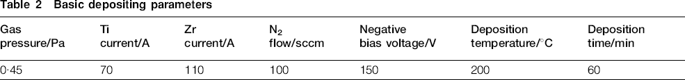
Microstructures of ZrTiN films
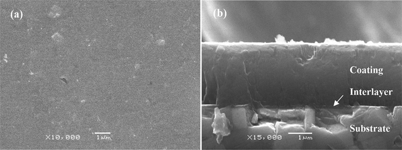
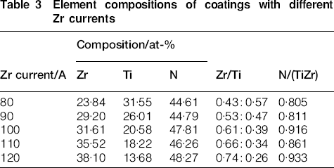
Figure 1 shows the surface and cross-section morphology of the sample at Zr current of 110 A. It can be seen that the film exhibits a dense and fine grained structure with no obviously columnar growth structure, and the combination of film and substrate is compact. It also shows that the thickness of the coating is ∼2·5 μm. The distribution of N, Ti and Zr elements on the surface (Fig. 1a) of the coating is denoted in Fig. 2. It indicates that the N, Ti and Zr elements exist in the coating surface, and they are quite evenly distributed throughout the microstructure. Element compositions of the coatings with different Zr currents are also analysed by map scanning, as shown in Table 3. The ratios of Zr/Ti and N/(TiZr) are approximately crescent along with the increase in Zr current.
a surface and b cross-section morphology of ZrTiN film at Zr current of 110 A
Distribution of a N, b Ti and c Zr elements on surface of film
Element compositions of coatings with different Zr currents
It is known that (111) is the hardest orientation in transition metal nitride due to the fact that the Schmid factor is zero on all slip systems.15 However, the crystal direction is not the only factor that affects the microhardness. Figure 3 denotes the XRD patterns of ZrTiN coatings deposited with different Zr currents. The film is thin, and diffraction peaks of WC, TiC and Co contained in the substrate also exist. Diffraction patterns of ZrTiN coatings indicate that only the face centred cubic phase exists. The diffraction peak of (111) direction is the strongest among the observed diffraction peaks of (111), (200) and (311) crystal direction. There is a diffraction peak of ZrTi at 2θ of ∼33° when the Zr current is 100 A, and this may result from the metal droplet while depositing. As the Zr current increases, the diffraction angle of each diffraction peak decreases between the standard diffraction of TiN and ZrN. The lattice parameters of TiN and ZrN are 0·4242 and 0·4578 nm, as reported. The formation of substitutional solid solution results in a variation in lattice parameters of ZrTiN films compared with pure TiN and ZrN. If the coating is described as ZrxTi1−xN, x changes from 0·43 to 0·74 as the Zr current increases from 80 to 120 A. The lattice parameters of ZrTiN films are calculated and plotted in Fig. 4 as functions of x in ZrxTi1−xN. It can be seen that the lattice parameter changes approximately linearly in keeping with Vegard's law. The lattice parameters calculated from the (111) direction are distinctly larger than that from (200). At the same time, the lattice parameters counted in this study are a little larger. This is perhaps because of the internal stress and interior defects or void of the crystal. All the grain sizes of the films are ∼9 nm as estimated using the Debye–Scherrer formula.
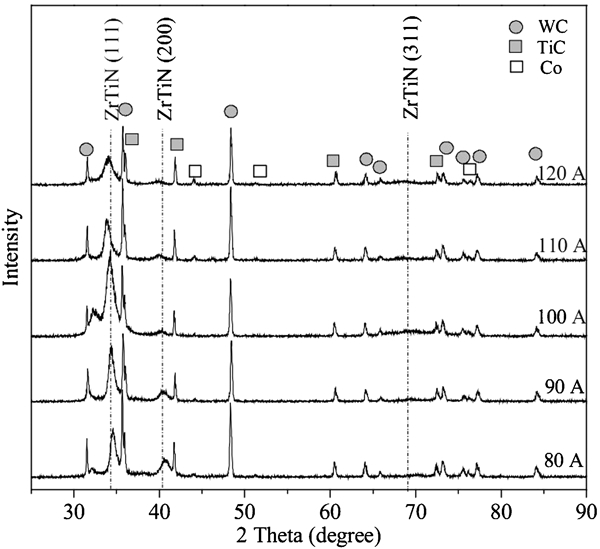
Patterns (XRD) of ZrTiN coatings deposited under various Zr currents
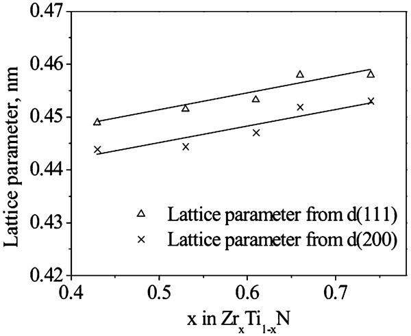
Lattice parameters for ZrxTi1−xN films deposited under various Zr currents
Properties of ZrTiN films
Component differences induce the distinct properties of ZrTiN coatings. Microhardness and adhesive strength with different Zr currents are summarised in Fig. 5. The results indicate that ZrTiN coatings exist at higher microhardness value than their binary counterparts TiN and ZrN (∼23 GPa) measured in the same conditions. High microhardness is on account of the solid solution strengthening,20 which has distortion of the periodic lattice. The variation in microhardness of ZrTiN coatings with respect to Zr current is inconspicuous. The highest microhardness value (29·2 GPa) is observed at Zr current of 100 A. Some literatures show that nanograin size plays an important role in the hardness of the material,21 but the hardness of ZrTiN coatings is mainly decided by many other factors, such as preferred orientation, crystal quality, composition of ZrxTiyNz, etc. Commonly, the poor adhesive strength is consistent with the high microhardness because of the high residual stress engendered by solid solution strengthening. As shown in Fig. 5, the adhesive strength increases with Zr current increasing. The film deposited at the Zr current of 110 A possesses both high adhesive strength and microhardness.
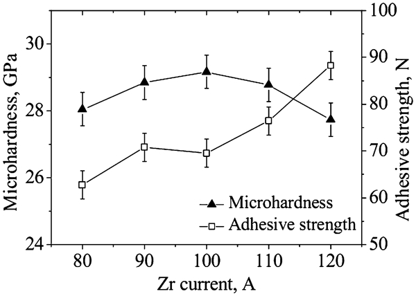
Microhardness and adhesive strength with respect to Zr currents
Effect of nitrogen flowrate
The nitrogen flowrate varies from 80 to 160 sccm with each increase of 20 sccm, and the other parameters are as follows: Zr current of 110 A, Ti current of 70 A, negative bias voltage of 150 V and deposition temperature of 200°C.
Microstructures of ZrTiN films
The element compositions of coatings with different nitrogen flowrates are denoted in Table 4. The ratio of Zr/Ti is not constant, although the Ti and Zr currents are fixed. The minimum Zr/Ti ratio appears at 120 sccm. The variation in N/(TiZr) ratio is on the contrary of Zr/Ti ratio, and the maximum N/(TiZr) ratio also appears at 120 sccm. This tendency is receivable because the different nitrogen flowrates will alter the partial pressure of argon, which is used to sputter the targets or to aid arc ignition.
Element compositions of coatings with different nitrogen flowrates
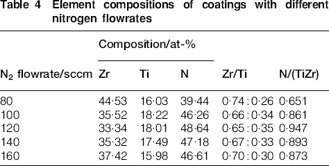
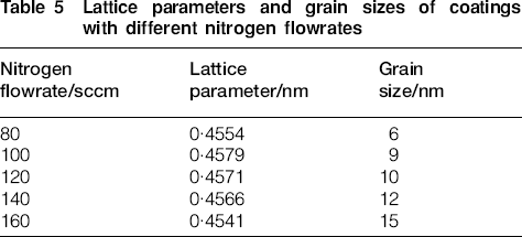
Figure 6 shows the XRD patterns of ZrTiN coatings deposited with different nitrogen flowrates. The diffraction peak of (111) direction is the strongest among the observed diffraction peaks of (111), (200) and (311) crystal direction for the coatings, except for nitrogen flowrate of 160 sccm with (200) direction. The diffraction peak of (111) direction is the strongest when the nitrogen flowrate is 100 sccm. As the nitrogen flowrate increases, the diffraction peak of (200) increases, and diffraction peak of (311) direction changes a little. In conclusion, the preferred orientation changes from (111) to (200) with increases in nitrogen flowrate from 80 to 160 sccm. Table 5 shows the lattice parameters and grain sizes of coatings obtained from XRD analysis. It can be seen that the lattice parameters change inconspicuously compared with that of Zr current. The grain size of the film increases from 6 to 15 nm when the nitrogen flowrate increases. This is because the crystallisation condition improves with the increase in nitrogen partial pressure, and this will cause the increase in average grain size.
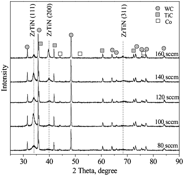
Patterns (XRD) of ZrTiN coatings deposited under various nitrogen flowrates
Lattice parameters and grain sizes of coatings with different nitrogen flowrates
Properties of ZrTiN films
The increase in nitrogen flowrate will decrease the partial pressure of argon, which is used to sputter the targets or to aid arc ignition; if the nitrogen flowrate unceasingly increases to 160 sccm, then the average grain size increases and the microstructure of the coatings become not so compact. This will lead to the declines in hardness and adhesive strength, as given in Fig. 7. The variation in microhardness of ZrTiN coatings with respect to nitrogen flowrates is conspicuous. The highest microhardness value (29·5 GPa) is observed at the nitrogen flowrate of 120 sccm. The coating deposited at the nitrogen flowrate of 140 sccm possesses the highest adhesive strength of ∼86·2 N, with a microhardness of 28·5 GPa.
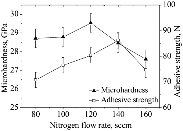
Microhardness and adhesive strength with respect to nitrogen flowrates
Effect of deposition temperature
The deposition temperatures chosen in this study are 100, 150, 200 and 250°C respectively. The other parameters are as follows: nitrogen flowrate of 140 sccm, Zr current of 110 A, Ti current of 70 A and negative bias voltage of 150 V.
Microstructures of ZrTiN films
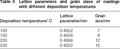
The preferred orientation of the ZrTiN coating is evidently affected by the deposition temperature, as illustrated in Fig. 8. Except for the deposition temperature 250°C with (200) direction, the diffraction peak of (111) direction is the strongest among the (111), (200) and (311) crystal directions. The diffraction peak of (111) direction is the strongest when the deposition temperature is 200°C. As the deposition temperature rises, the diffraction peak of (111) increases first and then decreased, while that of (200) increases. In conclusion, the preferred orientation changes from (111) to (200) while raising the deposition temperature. The lattice parameters and grain sizes of coatings obtained from XRD analysis deposited at different deposition temperatures are demonstrated in Table 6. The lattice parameters change inconspicuously compared with that of Zr current. The grain size of the films increases from 7 to 15 nm when the deposition temperature rises from 100 to 250°C. For most polycrystalline materials, the average grain size increases with elevating temperature. A high deposition temperature will also result in the coarsening of the crystallisation performance of ZrTiN while depositing.
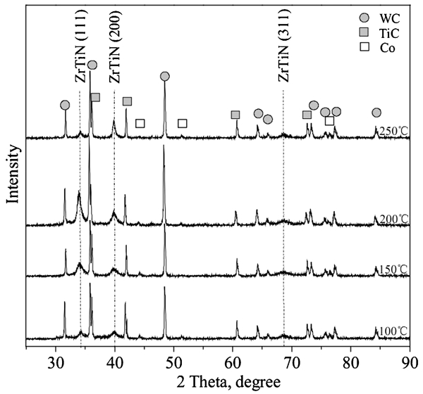
Patterns (XRD) of ZrTiN coatings deposited under various deposition temperatures
Lattice parameters and grain sizes of coatings with different deposition temperatures
Properties of ZrTiN films
Microhardness and adhesive strength with different deposition temperatures are exhibited in Fig. 9. As the temperature rises, the energy and activity of ion that deposited on the substrate increase. Some particles that have been deposited on the substrate will detach again from the surface if the energy is high enough. If the temperature is low, then the energy and activity of the ion are small, and the coating is incompact. This leads to poor microhardness and adhesive strength. As the deposition temperature rises, the energy and activity of the ion increase, and the properties of the coatings improve. Whereas when the deposition temperature rises too high, the energy of the ion is too great to form a stable film. This will also cause the deterioration of the properties. The preferable comprehensive mechanical properties of the coating appear at the deposition temperature of 200°C with a microhardness of 28·5 GPa and an adhesive strength of 86·2 N.
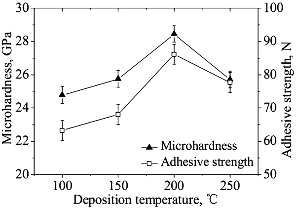
Microhardness and adhesive strength with respect to deposition temperature
Effect of negative bias voltage
We investigate the microstructures and properties of coatings under negative bias voltages between 50 and 550 V with each increase of 100 V while keeping the other parameters constant as follows: nitrogen flowrate of 140 sccm, Zr current of 110 A, Ti current of 70 A and deposition temperature of 200°C.
Microstructures of ZrTiN films
It can be obviously seen from Fig. 10 that the surface morphology of the film is also dependent on the negative bias voltage. As the negative bias voltage increases, the surface quality of the coatings debases, and dents or even large concaves come into being if the negative bias voltage is high enough, as shown in Fig. 10d–f. This is because of the tremendous ion bombardment effect on the coating surface while depositing if the negative bias voltage is too high.
Surface micrographs of films deposited under various substrate bias voltages: a 50 V; b 150 V; c 250 V; d 350 V; e 450 V; f 550 V
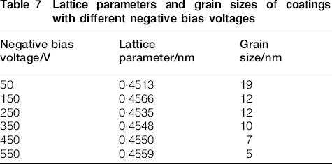
The preferred orientation of the ZrTiN film is evidently affected by the negative bias voltage, as revealed in Fig. 11. If the negative bias voltage is higher than 250 V, then a new crystal orientation (220) is detected compared with other parameters. If the negative bias voltage is 550 V, then all the diffraction peaks become weak, including the (220) orientation. This is because the energy distribution of ion bombarded on the substrate is high, and this may conduce to the amorphisation of ZrTiN while depositing. The preferred orientation changes from (200) to (111) and then (220) direction as the substrate bias voltage increases. The lattice parameters and grain sizes of coatings obtained from XRD analysis are shown in Table 7. It can be seen that the lattice parameter increases while the grain size decreases approximately linearly under different negative bias voltages. The tremendous bombardment effect while depositing at high negative bias voltage will lead to the distortion of crystal lattice and the grain refinement of ZrTiN.
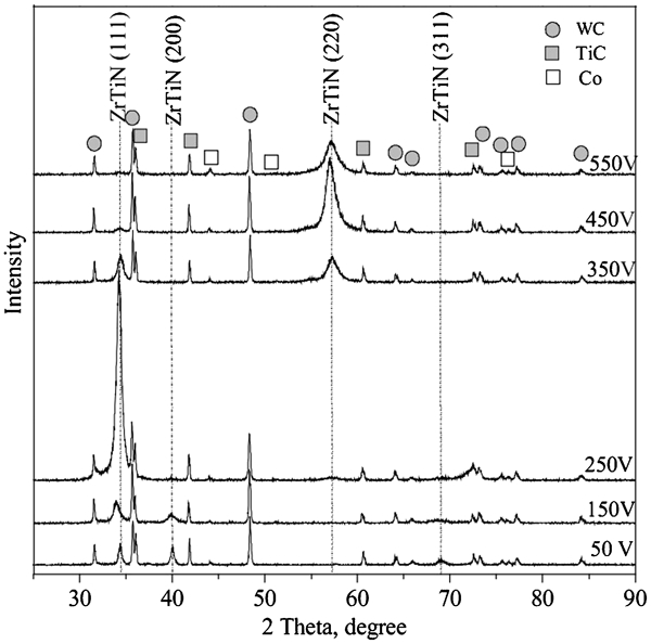
Patterns (XRD) of ZrTiN coatings deposited under various negative bias voltages
Lattice parameters and grain sizes of coatings with different negative bias voltages
Properties of ZrTiN films
The microhardness and adhesive strength of ZrTiN coatings as a function of negative bias voltage are indicated in Fig. 12. Increasing the negative bias voltage from 50 to 250 V leads to the reinforcement of crystal grain and (111) crystal orientation. The highest microhardness (∼30·4 GPa) is observed at the negative bias voltage of 250 V. If the bias voltage exceeds 250 V, then dents or large concaves are engendered in the coatings. Furthermore, (220) orientation forms and substitutes the (111) orientation. This will cause a decrease in microhardness. We should also pay attention to the high temperature annealing effect of high energy ion bombardment22 when the bias voltage is high. Simultaneously, the increase in residual stress and augmentation of dents or concaves will perhaps cause the decrease in adhesive strength. The preferable comprehensive mechanical properties of the films appear at the negative bias voltage of 250 V with a microhardness of 30·4 GPa and an adhesive strength of 84·1 N.
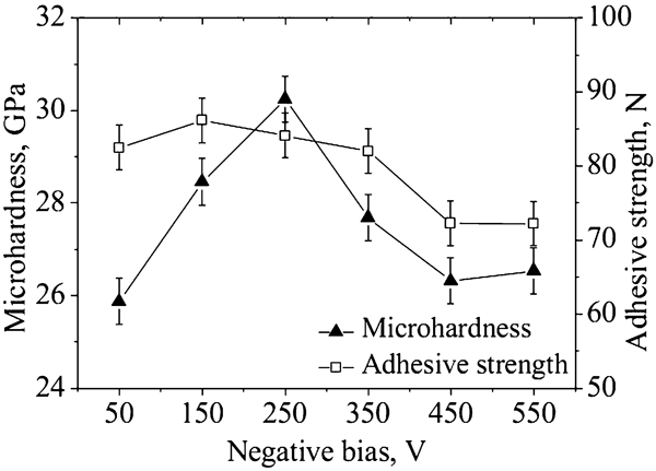
Microhardness and adhesive strength with respect to negative bias voltages
Conclusion
The PVD ZrTiN hard coatings are deposited on WC/TiC/Co cemented carbide substrate by multi arc ion plating. This study presents a detailed analysis of the effect of four parameters on the microstructures and properties of ZrTiN films respectively. The major conclusions can be summarised as follows.
The lattice parameter changes approximately linearly in keeping with Vegard's law under different Zr currents. The diffraction peak of (111) direction is the strongest among the observed diffraction peaks of (111), (200) and (311) crystal direction. The adhesive strength increases as Zr current increases.
As the nitrogen flowrate increases, the preferred orientation changes from (111) to (200). The lattice parameters change inconspicuously while the grain size of the film increases from 6 to 15 nm. The coating deposited at a nitrogen flowrate of 140 sccm possesses both high adhesive strength and microhardness.
The preferred orientation changes from (111) to (200), while the deposition temperature rises from 100 to 250°C. The grain size of the film increases from 7 to 15 nm. Preferable comprehensive mechanical properties of the coatings appear at the deposition temperature of 200°C with a microhardness of 28·5 GPa and an adhesive strength of 86·2 N.
As the negative bias voltage increases, the surface quality of ZrTiN coatings debases. A new crystal orientation (220) is detected, and the preferred orientation changes from (200) to (111) and then (220). The lattice parameter increases while the grain size decreases approximately linearly. The coating deposited at the negative bias voltage of 250 V possesses the highest microhardness of 30·4 GPa and an eximious adhesive strength of 84·1 N.
Footnotes
Acknowledgements
This work was supported by ‘the National Natural Science Foundation of China (grant no. 51075237)’, ‘the Taishan Scholar Program Foundation of Shandong’, ‘the Outstanding Young Scholar Science Foundation of Shandong (grant no. JQ200917)’ and ‘the National Basic Research Program of China (grant no. 2009CB724402)’.