
Abstract
In this study, ultrahigh vacuum chemical vapour deposition was employed to deposit multilayered silicon–germanium (SiGe) films. Subsequently, we take those samples for ex situ thermal treatments in the furnace system (400 and 500°C). The periodic multilayer SiGe with different annealing conditions measured by a commercial nanoindenter observed the slight increase in hardness. The cross-section profile and the microstructure of SiGe multilayer films were characterised by means of atomic force microscopy and transmission electron microscopy. The effect of the thermodynamics of the thin film/substrate system is evidenced by annealing treatment. It is demonstrated that the SiGe multilayer films are more susceptible to plastic deformation while annealing treatments are carried out. The misfit dislocations in the critical pile-up event were observed in the periodical SiGe multilayer that can be relaxed at thermal annealing, thus providing the nanomechanical performance.
Introduction
Silicon–germanium (SiGe) has been paid much attention due to the adjustable bandgaps, enhanced carrier mobility and higher dopant solubility than that of pure Si. In fact, SiGe alloy is competitive with III–V alloy, which makes it compatible with Si processing and low cost to integrate with high speed Si based technology applications.1 – 3 Si1−xGex alloys not only are promising materials for progressive components but also play an important role in the microelectronic device, like heterojunction bipolar transistors and hetero field effect transistors. In addition, the mechanical loads of mobile systems can arise from shock loading during fabrication and handling processes, leading to mechanical damage of their desired characteristics. The advent of nanoindentation instruments has led to a greater understanding of the underlying principles that affect contact loading and related phenomena. Nanometre scale nanoindentation has been used widely to investigate the deformation mechanisms of various semiconductors.
Herein, SiGe alloy is usually limited or compromised in application by the fact that for a given lattice mismatch strain in the heterostructure, a critical thickness exists above which it is energetically favourable for the lattice mismatch strain to be accommodated by an interfacial misfit dislocation.4,5 The implication of the degree of Si/Ge interdiffusion in the microstructure is difficult to decide because it was caused by several factors, including Ge content, temperature, etc.6,7 As noted above, the lattice mismatch between SiGe and Si substrate can serve as crystal defects, such as misfit dislocations and threading dislocations in the microstructure, which can result in the degradation of device qualities, i.e. it is suggested that the main misfit dislocations may exist at several interfaces and thread through the layers. In this perspective, the occurrences of misfit dislocations tend to exist on the edge component that results in active areas of the device.8,9 In this case, the quality configuration corresponding to interfacial misfit dislocation on the SiGe epilayer is required, and crystal defects and non-uniform compositions are undesirable.10,11 Accordingly, the model of multilayer became useful systems that can be designed to improve the hardness of the films. It is speculated that the hardness of these multilayer films was significantly improved in comparison with that of one monolayer. Recently, in the field of monolithic integration of Si based micro- and optoelectronic devices, the multilayer SiGe/Si system has attracted wide interest.12 In order to distinguish films from substrates, nanoindentation techniques are important tools for the measurement of mechanical properties, such as elastic modulus E and hardness H.13 – 18 With regard to the restriction of dislocation movement on the inner film, the SiGe multilayer film is desired to make it clearly in the hardness enhancement mechanism. From He et al.,19 high quality relaxed SiGe films are introduced to compare single and multilayers grown epitaxially by ultrahigh vacuum chemical vapour deposition (UHV/CVD) methods. We also study the issue of high annealing temperature (800–1000°C) treatment. The multilayer films relax to reduce the strain energy; the restricted dislocation movement serves an active role at the interfaces.20 Truly, the Si can acquire the larger atomic spacing of the underlying SiGe and become strained; therefore, it is important to find the interface science of epitaxial SiGe films. That is to say, it is an attractive approach by means of direct observation and measurement on the contact area during indentation during complex elastic and plastic deformation processes. In this study, it is important to note the stress and deformation fields in the vicinity of the contact; nevertheless, it is not an easy task to obtain due to the non-uniformity of SiGe/Si films. Furthermore, the annealing treated SiGe film is still not fully understood yet in the periodical structure to undergo from the indentation process. From the annealing treatment, it has potential to estimate the reliability character of periodical SiGe multilayered structure by means of the quantitative method. The purpose of this work is to present the recent study on the multilayer structure by nanoindentation technique and its applications.
The aim of this study is to investigate the nanomechanical properties of SiGe multilayer films deposited by UHV/CVD system and annealing treated at various temperatures. Additionally, a discussion of the indentation mechanisms on a nanometre scale and the influence of steep doping of stable Ge profiles are presented.
Experimental
SiGe multilayer films with varying degrees of initial strain relaxation were grown by UHV/CVD system; the deposition process was described as follows. First, the p type Si(1 0 0) wafers were prepared by a standard Radio Corporation of American clean and an HF/H2O (1∶50) bath for 15 s. The samples were simultaneously introduced into the load lock chamber of the UHV/CVD system. Afterwards, a 120 nm thick Si0·8Ge0·2 layer was deposited at 500°C for ∼43 min from pure SiH4 (85 sccm) and GeH4 (15 sccm) mixing (Ge concentration x = 20), the rate of deposition is 2·8 nm min−1 and the vacuum is achieved at 10−7 mbar. Second, A 10 nm thick Si buffer layer was deposited on the Si substrate at 500°C for 100 min from pure SiH4 ( sccm) gas, the rate of deposition is 0·1 nm min−1 and the vacuum is achieved at 10−7 mbar. Meanwhile, the SiGe and Si buffer layers were deposited following four period cycles, and the structures were terminated by a 10 nm thick Si cap layer (∼530 nm in the total thickness). Third, in the annealing treatment, the SiGe multilayer films were ex situ endured thermal treatments in furnace on N2 gas for 10 min (400 and 500°C).
From the atomic force microscope (AFM) analysis, we mainly investigated three-dimensional pattern images and section analysis while the nanoindenter is made. In addition, transmission electron microscopy (TEM) samples were prepared within mechanical polishing down to 20–30 μm, followed by Ar ion milling to electron transparency.21 The observations were made at 200 kV. Subsequent hardness and elastic modulus of the SiGe multilayer films were studied using a nanoindenter XP instrument (MTS Cooperation, Nano Instruments Innovation Center, Oak Ridge, TN, USA). The continuous contact stiffness measurement (CSM) mode, which is executed by superimposing small oscillations on the force signal to measure displacement responses, offers a direct measure of dynamic contact stiffness during the loading process in the indentation test and is insensitive to thermal drift.
Results and discussion
To investigate the nanomechanical properties by nanoindentation methods, it requires a detailed understanding of the information contained in the indentation loading and unloading curves. As usual, the intermixing alters the interfacial properties of the SiGe multilayer films and then degrades the film performance. The strain relaxed performance from annealing treatment can thus be provided. In Fig. 1, the same displacements of loading–unloading curves of the non-annealed (a) and annealed (b and c) SiGe multilayer films are illustrated. The discrepancy in the penetration depths of the samples is revealed obviously. Afterward, one can see that the non-annealed SiGe multilayer film is softer than that of the annealed ones due to the maximum penetration depth. It is observed that the H of the annealed SiGe multilayer films is higher than that of the non-annealed one because of less penetration depth. The nanoindentation is a useful technique in probing the characteristics of the films; we thus employ the CSM mode to discover the penetration depth dependence of E and H in SiGe multilayer films. Figure 2 shows the typical CSM results of SiGe multilayer films for non-annealed and annealed ones on Si substrate. In Fig. 2a, the effect of the substrate is evident from the contact depth dependence of H. For indentation depths up to ∼10 nm, the H increased as the indentation depth became deeper, which is usually attributed to the transition between purely elastic to elastoplastic contact, while H is actually the contact pressure. For indentation depths over 25 nm, the H of SiGe films remains constant. The E also followed a trend similar to that of the H, which is conformed at an indentation depth smaller than that for H (Fig. 2b). H and E were therefore concluded by averaging measurements at indentation depths from 100 to 200 nm, serving an adequate depth to indicate a fully developed plastic zone and meanwhile to avoid more substrate effects.22 It is suggested that the influence of the substrate is expected due to the experiments under a 10 mN peak load presented here (the penetration depth is ∼200 nm); the values do not exceed half of the film thickness (530 nm) since this substrate probably affects the values of the elastoplasticity coefficients.23 The measured H with SiGe multilayer films for non-annealed and annealed ones on the Si substrate were 12·9±0·3, 13·3±0·3 and 13·5±0·4 respectively; the measured E were 200±5·2, 198±4·2 and 195±4·0 GPa respectively. It is interesting to note that the H of the annealing SiGe multilayer films is slightly higher than non-annealing; otherwise, the E also slightly decreases under annealing treatment because it is in proportion to stiffness. It is suggested that the discrepancies within the SiGe multilayer films are owing to the enhanced activation energy, which is dependent of the kink model24 for dislocation glide.25,26
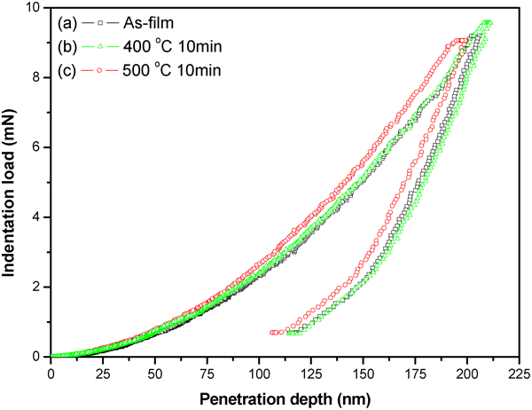
Load on sample plotted with respect to displacement into surface for SiGe multilayer films at various annealing treatments:
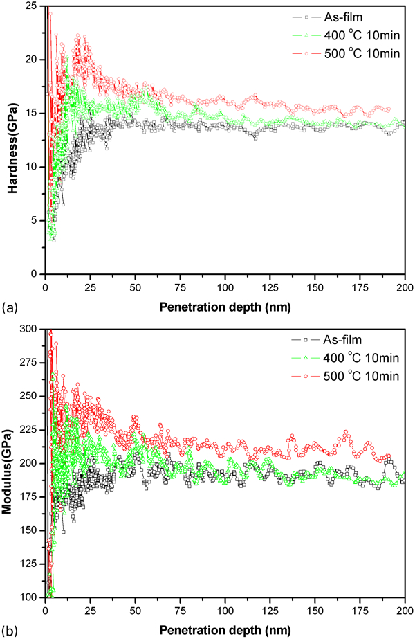
a elastic moduli and b hardness of SiGe thin film samples plotted with respect to indentation depth (those conditions are RT, 400°C and 500°C)
The AFM system was employed to investigate the annealing process of the SiGe multilayer films. It can be observed that the depth profiles are 746, 700 and 686 nm (Tg = RT, 400 and 500°C) from the cross-section analysis of the indenter region images (insert in Fig. 3), which implies that the Si1−xGex layers at increased annealing temperature have a stronger adhesion at the interface. It is evident that the epilayer–substrate combination corresponds to a softer epilayer (SiGe) on a harder Si substrate. The harder substrate, relatively difficult to indent, may support a severe resistance to plastic deformation of the films, which could change their response. Hence, we observe the nanoindentation deformation at 500°C within the shallow section profile, which may be due to the effect of the annealed treatment. From Tételin et al.,27 they suggest that the waved surfaces observed in multilayer films may be due to the two-dimensional germanium segregation on the surface during the growing or annealing process at the temperature of <600°C. He et al.19 have discovered that SiGe multilayer films are subjected to the compression of shear stress emerging at the SiGe multilayer film interface, and the annealing samples under the influence of internal mechanical properties were demonstrated. The observation of dislocation glides for the undergone dislocation nucleation is evidenced. This phenomenon concentration at the interface and the films tend to leading dislocation in order to release the inner stress of the SiGe multilayer films. Herein, the varying microstructures of SiGe films before and after annealing treatments are estimated by cross-sectional TEM examination. From previous studies,19,20 the same sample of non-annealed SiGe multilayer films was used here. In Fig. 4a, the profile of non-annealed SiGe films displayed that virtually no misfit dislocations and native dislocations have been observed. Figure 4a also reveals the high resolution image of pure interface of non-annealed SiGe films. Figure 4b reveals the unstable interface of SiGe multilayer films while the sample endured annealing treatment at 400°C. A low density of short misfit segments is found based on the interdiffusion from the misfit dislocations. Thus, we observe that the amorphous Si buffer layer/SiGe layers are embedded with each other and mainly crystalline. In Fig. 4c, one can compare that the dislocation event is clearly at the SiGe multilayer films while the annealing temperature is up to 500°C. It is suggested that both the misfit segments and the activated nuclei occur during the increase in annealed temperature.19 Herein, the work demonstrates that the nucleation events and misfit segments are independent while in thermally activated condition in the SiGe multilayer films. In the results of the TEM profile, one can observe that the nucleation seed is starting at each interface of the SiGe multilayer films (Fig. 4a) and thus induces a higher density of misfit dislocations (Fig. 4b and c). In our experimental results, however, the high density of misfit dislocations can be aggregated between SiGe multilayer films after annealing. In a recent article,20 the nanotribological behaviour of multilayer SiGe films might be due to the restricted dislocation movement from the active interfaces after annealing. The microstructure of the SiGe films/Si buffer was strongly intermixed during the annealing process, consistent with the results obtained through TEM imaging. It is suggested that the relative defects may induce the change in mechanical properties of the SiGe multilayer films in experimental results. The reproduction of corner dislocations was reported in the SiGe structures grown by UHV/CVD method, which were conducted by a modified Frank–Reed mechanism.4 The result conducted that the restriction of dislocation movement was embedded under SiGe multilayer films, as shown in Fig. 4. In short, those results demonstrate that the SiGe multilayer films are more susceptible to plastic deformation while annealing treatments are carried out; accordingly, multilayer films will relax and reduce the strain energy at the same time.
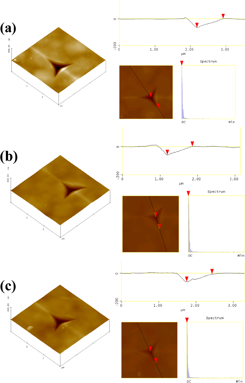
Images (AFM) of indenter region of samples:
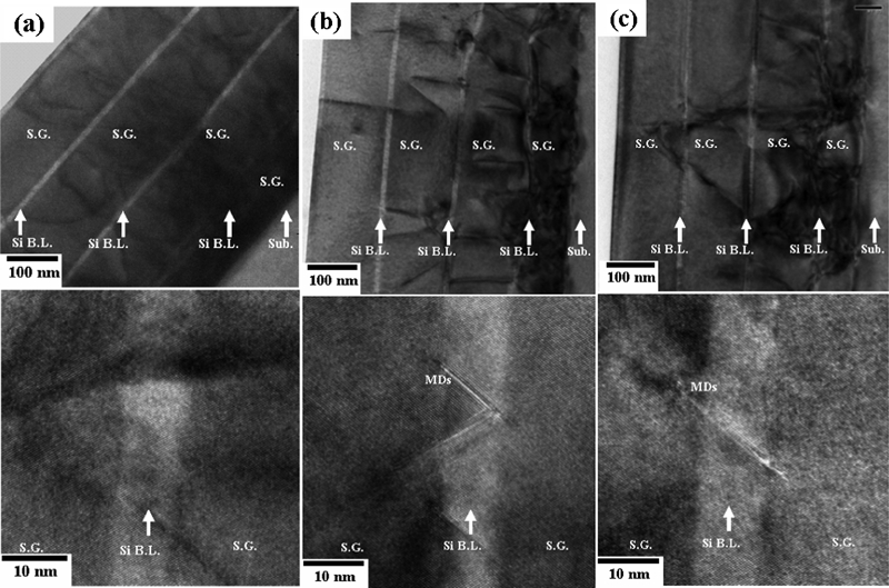
Cross-sectional TEM image of SiGe thin film samples (S.G.: SiGe layer; Si cap: Si capping; Si BL: Si buffer layer; Sub: Si subtract; MDs: misfit dislocations):
Conclusion
In our experiment using the growth of high quality SiGe multilayer structures as a sample, we have presented the effect of restriction of dislocation movement on the nanomechanical properties while the annealing is made. Both the dislocation multiplication and the dislocation nucleation may rise from the annealing treatment, which is observable at cross-sectional TEM analysis. From the nanoindentation tests, the hardness is enhanced from strain relaxation after thermodynamic treatment; the more susceptible plastic deformation is caused by dislocation induced additional strain. We suggest that the effects of the dislocation glide and the dislocation pinning at each interlayer play an important role that serve the hardening mechanisms. It is demonstrated that the quantitative stress was inside the layer; the production of dislocations in the microstructure was evidenced in detail.
Footnotes
Acknowledgements
The authors would like to thank Dr H.-C. Wen and Dr D. Lian for helping with the sample preparation and TEM image support that aided the great technical support and the kind useful discussions of the manuscript. This research was supported in part by the National Nano Device Laboratories under contract nos. NDL-97-C05G-087 and NDL99-C03S-039, and Chin-Yi University of Technology under contract nos. NCUT11-REM-004