
Abstract
This paper describes the mechanisms of Berkovich nanoindentation induced mechanical deformation of GaN films under various loading–reloading cycles, analysed using cathodoluminescence, atomic force microscopy (AFM) and SEM. The AFM and SEM studies revealed that bursts, due to the nucleation of dislocations, occurred after nine loading–reloading cycles; these bursts resulted in incipient slip bands and/or the to and fro motion of mobile dislocations under the stress field. Cathodoluminescence analysis indicated the generation of individual dislocations and residual deformation on the GaN film; the decrease in hardness H can be used to determine the material properties of films undergoing repeated loading–reloading cycles.
Introduction
Epitaxial III-nitride materials (GaN, ZnO and InN) have attracted much attention over the last decade because of their expected high performance.1 – 3 The reliability of a semiconductor device is dependent not only on its surface contacts but also on its degrees of cracking, film delamination and propagation of dislocations. GaN films have been the particular focus of attention because of their potential use in short wavelength optoelectronic devices, optical detectors and semiconductor lasers.4,5
The deformation mechanisms of GaN are, therefore, of significant technological importance, with contact induced damage, cracking and epilayer delamination being of particular interest. Thin films of GaN typically exhibit mismatched lattice constants and thermal expansion coefficients because of high dislocation densities and produce high residual strain during the post-growth process; all of these factors influence the mechanical properties.6 – 12 Discontinuities in the indentation load–penetration curves have been reported for a series of brittle semiconductor materials (Si, Ge, InP and GaAs). The observation of such discontinuities might be an indicator of physical deformation and/or phase transformations.13,14
The successful fabrication of devices incorporating epitaxial GaN films requires a thorough understanding of their mechanical, optical and electrical behaviour; contact loading during processing or packaging can degrade the quality of these devices. Because it is important to solve the problems arising from residual stress–strain introduced by heteroepitaxial films, there is significant interest in developing methods for the mechanical characterisation of GaN films. Several methods are available for growing thick GaN films and then separating them from their substrates.15 – 19 In such cases, determining the precise mechanical properties of GaN films remains a challenging task.
The presence of misfit dislocations at the interfaces of GaN films appears to play a role in determining the carrier mobility and luminescence efficiency.2,20 Nanoindentation is a manipulation process that can be used to analyse the mechanical properties (hardness, elastic modulus, creep resistance, fracture toughness and adhesion) of films.21 – 29 Plots of indentation load versus displacement are typically obtained to understand these miscellaneous properties.27,29 GaN films and bulk single crystals have been investigated to determine the role of the slip band movement and the dislocation nucleation mechanism during pop-in events. Basu et al.16 concluded that basal slips and non-linear elastic kinking are initiated when both the C and A orientations of GaN films are indented; their study provided a detailed understanding of machining damage. Although GaN films have been the subject of pop-in studies,30 the behaviour of recrystallised GaN films on c axis sapphire substrates under cyclic indentation remains poorly understood.
In this study, we employed nanoindentation techniques to discover the response of GaN films under loading–reloading cycles. Cathodoluminescence (CL) measurements allowed us to physically assess the degree of lattice disorder of the samples. We used atomic force microscopy (AFM) to investigate the surface regions of these GaN films.
Experimental
GaN films were grown epitaxially on c axis (0 0 0 1) sapphire plane substrates through metal–organic chemical vapour deposition (MOCVD). To fabricate GaN films, a 10 nm thick AlN buffer layer was first grown on the c axis (0 0 0 1) sapphire substrate and then GaN films (thickness, ∼10 μm) were grown on top of the buffer layer through MOCVD at 1100°C using triethylgallium, trimethylaluminium and ammonia as the gallium, aluminium and nitrogen atom sources respectively.
The mechanical properties of the GaN films were tested using a Nano Indenter XP nanoindentation system (MTS Corporation, Nano Instruments Innovation Center, TN, USA), equipped with a Berkovich indenter tip (radius of curvature, 50 nm), in the load controlled indentation mode with variation of the loading–reloading cycle number; each indentation was separated by 30 μm to avoid possible interference between neighbouring indents. The typical nanoindentation load–displacement conditions for the GaN film were referenced from the literature.20 The testing process followed a trapezoidal loading profile with a typical peak load hold time of 5 s and a loading rate of 10 mN s–1 at a constant load of 50 mN. One cycle penetration depth was performed while varying the number of loading–reloading indentation cycles (1, 3, 6 or 9 times) to characterise the mechanical deformation of GaN crystals. Ten indentations were made on each loading–reloading condition; the results presented herein are averages. The analytical method developed by Oliver and Pharr31 was adopted to determine the hardness H of the GaN films from the load–displacement curves.
The nanoindentation induced crack morphologies of the GaN films were examined through tapping mode AFM using a Veeco D5000 atomic force microscope and field emission SEM using a JEOL JSM-7001F field emission scanning electron microscope.
The nanoindentation induced mechanical deformations of the GaN films were characterised using a CL apparatus (HORIBA). Room temperature CL measurements and CL mapping were also performed using the JEOL JSM-7001F field emission scanning electron microscope. An electron beam energy of 20 keV was selected to excite the GaN surface. The CL light was dispersed using a 2400 nm grating spectrometer and detected by a liquid N2 cooled charge coupled device. The CL spectra were recorded from GaN samples in real time at a fixed electron beam energy of 20 keV. The corresponding CL image from the surface was displayed on video monitors. The CL images were recorded with the total emitted integral (panchromatic) CL as well as with light of a fixed spectral wavelength (550 nm) using a suitable charge coupled device.
Results and discussion
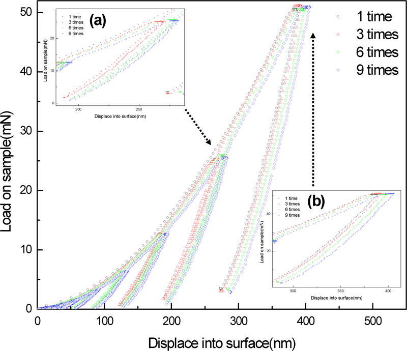
To provide an accurate accounting of the multiple discontinuities indentation of GaN films, we examined the effects of the loading–reloading process. Figure 1 presents the load–displacement P–h curve recorded during the indentation process; it reached a maximum indentation load of 50 mN. We observed that the typical plot of cycle number versus penetration depth of GaN film (Fig. 1, insert) exhibited multiple discontinuities during the indentation process (indicated by the arrows). Multiple pop-in behaviour of hexagonal structures of GaN films has been observed previously,25 suggesting that the indentation induced deformation mechanism of GaN films involves nucleation and propagation of dislocations. Figure 2 displays the typical effects of loading–unloading and unloading–reloading indentation cycles (3, 6 and 9 times); we obtained discordant curves. Irregularities appeared in the course of plastic deformation, characterised by the multiple discontinuities at certain penetration depths, for the unloading–reloading process (indicated by the arrows); the curve implies a trend of gradual elastic deformation. A similar report32 of the cyclic nanoindentation P–h curves of GaN test samples also revealed irregularities, the so called multiple pop in events, during loading in the penetration depth. The local displacement of 200–300 nm (Fig. 2, insert a) reveals a slight hysteresis loop dependence when each nanoindentation process maintained a peak load hold time of 5 s. Wen et al.25 and Jian reported,32 that the cyclic nanoindentation P–h curves of GaN films featured prominent multiple pop-ins, which were attributed to the motion of dislocation nucleation. It is speculated that more deleterious effects arise during multiple unloading–reloading; strain relaxing can also be observed. Hysteresis loops were evidenced due to the higher elastic modulus resulting from the increased number of nanoindentation cycles. We also observed a larger deviation in the P–h curves of the GaN films that had been subjected to unloading–reloading cycles (Fig. 2, insert b).
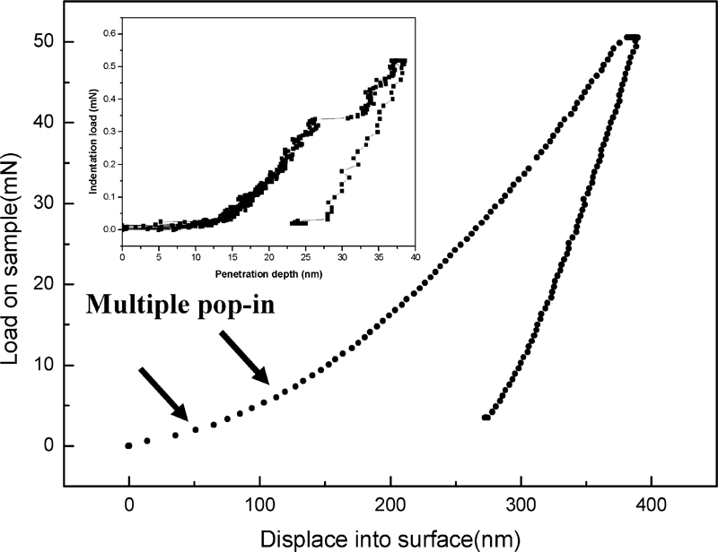
Load–displacement P–h curve recorded during indentation process; it reached maximum indentation load of 50 mN
Plots of load with respect to penetration depth of GaN film
In the P–h curves recorded after 1, 3, 6 and 9 cycles, the values of H of the GaN films on the c axis sapphire substrate were 15·55±0·1, 16·25±0·2, 16·55±0·2 and 16·89±0·2 GPa respectively. The listed values of H are consistent with those reported by Jian et al.33 We found that the strain hardening of GaN, partially induced from the penetration depth, had increased slightly. In addition, we attribute the hysteresis loops as arising from the volume change upon the reverse phase transformation of the GaN films, resulting either in a pop-out (or a kink back) or in a slope change (elbow) of the unloading part of the load–displacement curve. The changing slope of the elastic part of the loading curve during cyclic indentation can be used to confirm the occurrence of a phase transformation during indentation. In previous studies, GaN tended to crystallise into the wurtzite structure; theoretical studies,34 which have been confirmed experimentally,35 have concluded, however, that GaN undergoes a phase transformation into the rock salt structure under hydrostatic pressure (∼50 GPa). We used AFM to examine the residual impressions of the loading–reloading indent marks to check for evidence of slipping, cracking and pile-up/sink in. Figure 3a displays an AFM image of a sample subjected to typical nanoindentation conditions to maintain a maximum load of 50 mN. Slight activation of a pyramidal slip appears near the indent mark in the GaN films. A comparison of the effects of the number of loading–reloading cycles, determined from AFM images, revealed that nine unloading–reloading cycles provided a gradation of the protrusion case and some pyramidal slip nucleation in the cross profile (Fig. 3b). The GaN films/c axis sapphire system can interact with the indenter tip to form a deformed zone; the threading dislocations then enter into the films at certain depths, thereafter causing the pop-in event. We conjecture that the mechanism of the event was caused by slip bands28,30 and/or dislocation nucleation.29 The section profile of the AFM image of the sample after nine loading–reloading cycles also revealed the presence of pyramidal slips and partial cracks from the residual indentation mark, even when the indentation depth was changed. The pop-in bursts appear to be related to the nucleation and movement of the dislocation sources, including lattice atoms and, possibly, the effects of crystallisation. These features contributed to massive material transfer below the indented zone as well as to the sides of the indent. Because soft GaN films grown epitaxially on hard sapphire substrates tend to exhibit differences in lattice parameters and thermal expansion coefficients, misfit strain might be introduced at the interface; this strain can be released by generating threading dislocations in the GaN films.23,24 In the present study, CL mapping observations provided evidence of dislocation activity and crack features at the free surface around the indentation. Figure 3c and d presents CL maps recorded at the free surface around the indentation, acquired at a wavelength of 367 nm, from GaN films indented under the typical conditions and under nine loading–reloading cycles respectively.
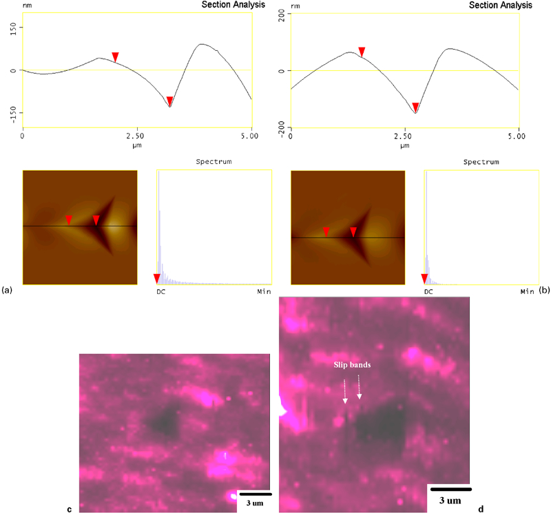
Images (AFM and SEM) of indented sapphire surfaces under a typical conditions and b nine loading–reloading cycles and CL maps acquired at wavelength of 367 nm from GaN films indented under c typical conditions and d nine loading–reloading cycles
We recorded CL spectra of GaN films that had been indented using both the typical conditions and nine reloading–reloading cycles. Figure 4 reveals a long wavelength band centred at 367 nm (∼3·4 eV); this band is usually attributed to the near band edge emission of GaN films. Near the surface, the luminescence–topography plots reveal the distribution of the respective luminescence centres and the edges of the indented area. The residual indentations were directly excited using the CL system. Upon proceeding from the typical conditions to the 9 cycle loadings of the indentation centre, the near band gap CL emission from the GaN films was suppressed dramatically because of induced defects and/or dislocations. Bradby et al.36 explored the extent of radial propagation of contact induced defects in ZnO; they observed dramatic suppression of the near band gap CL emission from the central regions of the residual indent impressions. To this end, dislocations act as non-radiative recombination centres that quench the luminescence locally. The CL spectrum of the indented area of the GaN films below the level of the critical ‘pop-in’ phenomenon revealed a slight reduction in the intensity of the CL emission, particularly for the very broad emission. Fernández et al.37 also noted that irradiation had an effect on the CL spectra, presumably as a result of complex formation or charge transfer processes caused by new point defects (2·0–2·2 eV) as well as higher concentrations of point defects in the deformed samples.
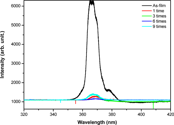
Cathodoluminescence spectra acquired at wavelength of 367 nm from GaN films indented under typical, three, six and nine loading–reloading cycles
These CL images reveal the distribution of indentation induced extended defects. The cube corner indenter form and these stretched defects reveal some radial symmetry of the stress field. Slip enhancement may have contributed to the formation of the observed crack. Bradby et al.36 studied the extent of radial propagation of contact induced defects in ZnO; they observed dramatic suppression of the CL near band gap emission from the central regions of the residual indent impressions. In fact, dislocations act as nonradiative recombination centres that quench the luminescence locally. Interestingly, the indented area below the propagation of dislocations of the GaN films was also observed in the CL image, revealing a detectable reduction in the intensity of the CL emission. Jian et al.38 reported that the primary deformation mechanism for GaN thin films grown on (0 0 0 1) sapphire substrates through MOCVD were dislocation nucleation and propagation along the easy slip systems. In this present study, after nine loading–reloading cycles, in which a large percentage of indentations were plastically deformed (Fig. 2), CL imaging could distinguish between indentations that had undergone several degrees of plastic deformation and indents that were purely in the elastic regime. Subsequently, we detected an observable CL impression only after the pile-up event, providing convincing evidence that the phenomenon involves the nucleation of slip as the deformation mode. Notably, the heavily strained features in the vicinity of the interface might not be just accidental artefacts that resulted from the sample preparation process; because of the excellent interface epitaxy between GaN film and substrate, they might provide evidence for the effects of nanoindentation extending into the sapphire substrate. A comparison of the AFM images and CL mapping analysis reveals a high compressive stress transition around the indentation regions of the GaN films. The initial deformation, elastic deformation and residual deformation of the GaN films were all evidenced after cyclic nanoindentation.
Conclusion
We have used nanoindentation and AFM techniques to analyse the cyclic loading–reloading deformation behaviour of the GaN films on c axis sapphire substrates. We suggest that the deformation of GaN films can be due to pop-in events, especially after nine loading–reloading cycles; thus, we observe deviations in the plots of penetration depth with respect to the number of nanoindentation cycles. In addition, we observed evidence for strain hardening of the GaN films upon increasing the number of nanoindentation cycles. We expect that the impression marks were based on multiple pop-in events revealed during the cyclic nanoindentation process; the transformation of the defects was also evident in the CL studies. Our results revealed that the typical loading–reloading indentation induced deformation mechanism in GaN films involved nucleation and propagation of dislocations, which corresponded to the extent of residual penetration or plastic deformation. Therefore, we make the following conclusions regarding the effect of the number of loading–reloading cycles on the indentation induced deformation mechanism.
Plastic deformation before each loading–reloading cycle is associated with the individual movement of a small number of new nucleation sites; large shear stress is quickly accumulated beneath the indenter tip.
When the local stress beneath the tip reaches a large value after repeated cycles, a burst of collective dislocation movement is activated on the slip system, resulting in a release of local stress.
Extensive interactions between the dislocations slipping along the GaN surface confined the slip bands, resulting in a pop-in event, due to the deformed and strain hardened lattice structure.
Footnotes
Acknowledgements
This research was supported in part by the Chin-Yi University of Technology under contract nos NCUT11-REM-004.