
Abstract
In this study, the influence of incremental rate of anodising current VIR on the crystal structure, surface roughness and corrosion resistance of anodic oxide films on Ti–10V–2Fe–3Al was studied using Raman spectroscopy, atomic force microscopy (AFM), electrochemical impedance spectroscopy (EIS) and potentiodynamic polarisation. The results showed that the surface roughness, crystal structure and electrochemical corrosion behaviour of anodic oxide films were remarkably affected by different VIR with regard to the change in the rate of anodising voltage. In addition, results of EIS and potentiodynamic polarisation revealed that the film that formed at VIR of 0··50 A min−1 had the highest corrosion resistance. Quantitative AFM characterisation showed good correlation between surface roughness and EIS results. Furthermore, results of Raman spectroscopy showed that the relative intensity of anatase and rutile had a tendency to increase with a decrease in VIR before reaching 0··50 A min−1.
Introduction
Titanium alloy Ti–10V–2Fe–3Al has widespread use in aerospace applications because of its excellent mechanical properties combined with satisfactory corrosion resistance behaviour.1 Titanium alloys exhibit a tendency to form a natural oxide layer on their surfaces. This layer protects against the harmful effects of harsh and aggressive environments and is responsible for the good corrosion resistance behaviour of the materials.2 However, there are several weak spots in the natural oxide layer that permit corrosive ions to penetrate the layer and cause material degradation. Anodic oxidation on titanium substrate is an often used surface treatment that increases the thickness and enhances the performance (resistance to wear, adhesion and corrosion) of the oxide film.
The electrochemical parameters of anodic oxidation significantly affect the growth behaviour and properties of the anodic oxide films that form on titanium alloys.3 – 7 Parameters that significantly affect the characteristics of the oxide film include electrolyte solution (concentration of reagents) and temperature as well as electrical parameters. The electrical parameters can alter the process of anion transfer during the process of anodisation. Moreover, electrical parameters determine the thickness, surface morphologies and microstructure of anodic coatings.8 Although several studies have been carried out to evaluate the effect of electrical parameters on the growth of anodic films following pulse anodic oxidation,9, 10 these studies have not paid much attention to the method of imposing the anodic current.
In a previously reported work by these authors, thick, uniform and non-transparent anodic oxide films were fabricated on the titanium alloy Ti–10V–2Fe–3Al using a pulse galvanostatic method.11 The present work aims to investigate the effect of the incremental rate of anodising current VIR on the growth, surface roughness and electrochemical corrosion resistance behaviour of the anodic oxide film that formed on the titanium alloy Ti–10V–2Fe–3Al. Correlations among VIR, film growth, surface roughness, crystal structure and electrochemical corrosion resistance behaviour of anodic oxide film were recognised on the basis of the results.
Experimental
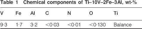
A forged block of titanium alloy Ti–10V–2Fe–3Al was cut into sheets measuring 100×30×3 mm. The nominal composition of the titanium alloy Ti–10V–2Fe–3Al is given in Table 1. Each sample was abraded with silicon carbide paper of successive grades from 300 to 1500 grit, then rinsed with acetone and deionised water and, finally, air dried.
Chemical components of Ti–10V–2Fe–3Al, wt-%
Anodic oxidation was carried out in a cell with a thermostat controlled water bath and a magnetic stirring apparatus. The prepared sample was used as anode, and a 1Cr18Ni9Ti stainless steel plate was used as cathode. An aqueous solution of sodium tartrate, which was prepared using analytical grade chemicals and deionised water, was the electrolyte for the reaction.
A pulse galvanostatic power supply, WMY-IV, was used, and the output mode of the power supply is shown in Fig. 1. The pulse of the power supply was unidirectional and exhibited a square wave. The ultimate value of the anodising current was set at 10 A. TLR denotes the time that the anodic current needs to increase to the specified value and was set at 2, 5, 10, 20 and 30 min; VIR was 5··0, 2··0, 1··0, 0··50 and 0··33 A min−1 and was changed in correlation with the duration of the reaction. Details of the fabrication conditions have been previously published.11
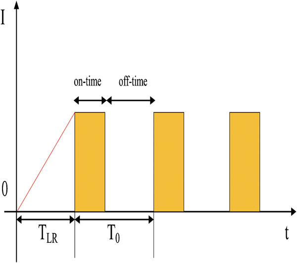
Output mode of power supply: TLR time anodic current needs to increase to specified value; T0 working period
The surface morphologies of the inner and outer anodised layers were evaluated using a scanning electron microscope (SEM, CS3400; Camscan). The surface roughness of the anodic oxide film was observed using a Dimension Icon atomic force microscope (AFM; Veeco, USA). The crystal structure of the anodic oxide film was determined by a Raman spectroscope (Raman; Yvon Jobin Horiba-HR800, using an He–Ne laser without filter at 633 nm).
Electrochemical measurements were carried out using a potentiostat/galvanostat (Parstat 2273; Princeton Applied Research) with a conventional three-electrode electrochemical cell, wherein the samples functioned as working electrode, a platinum plate was used as counter electrode and a saturated calomel electrode (SCE) was used as reference electrode. All experiments were carried out in 0··5 mol L−1 H2SO4 solution at 25±3°C.
The anodised electrodes were immersed in H2SO4 solution in open circuit conditions for 30 min before the electrochemical impedance spectroscopy (EIS) or potentiodynamic polarisation tests were conducted. The alternating current impedance spectra of the samples were obtained at the open circuit potential, with an amplitude of 10 mV and scan frequencies ranging from 100 kHz to 10 mHz (10 points/decade). Nyquist and Bode plots were obtained by curve fitting using a commercial software package called the Electrochemistry Power Suite. The EIS spectra were simulated using the ZSimpWin simulation software. The scanning rate of the potentiodynamic polarisation curve was 2 mV s−1, with a scanning range from −0··7 to 1··2 V(SCE).
Results
Development of film
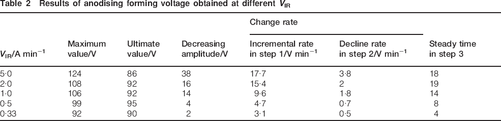
Figure 2 shows the change in anodising voltage as a function of anodising time at different VIR. Details of the results of the anodising voltage obtained at different VIR are shown in Table 2. The anodising process was classified into three steps for all of the samples. In the first step (step 1), the anodising voltage increased linearly with time up to the maximum anodising voltage. The maximum value and incremental rate of anodising voltage decreased when VIR decreased during this stage in the process. In the second step (step 2), the anodising voltage decreased proportionally with time of anodisation. The decreasing amplitude and declining rate of the anodising voltage decreased with the reduction of VIR. In the third step (step 3), the anodising voltage was approximately maintained at a steady value. The ultimate value increased when VIR decreased before reaching 0··50 A min−1. The steady time decreased with a decrease in VIR in step 3. This indicates that the ultimate value was greatest at VIR of 0··50 A min−1.
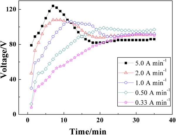
Anodising forming voltage with anodising time relation curves at different VIR
Results of anodising forming voltage obtained at different VIR
Atomic force microscopy characterisation
The AFM three-dimensional topographic representations for the samples at different VIR are depicted in Fig. 3. Figure 4 shows the variation of root mean square roughness Rq and average roughness Ra derived from the AFM analysis of the recorded area (20×20 μm). Values of Rq and Ra decreased with a decrease in VIR. The results indicated that the surface of the anodised samples gradually became smooth as VIR decreased before reaching 0··50 A min−1.

Images (AFM) of three-dimensional anodic oxide films at different VIR: a 5··0 A min−1; b 2··0 A min−1; c 1··0 A min−1; d 0··50 A min−1; e 0··33 A min−1
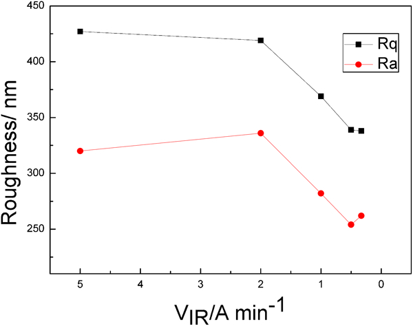
Surface roughness of anodic oxide films at different VIR
Raman spectroscopic characterisation
Figure 5 presents the Raman spectra of anodic oxide films formed on titanium alloy Ti–10V–2Fe–3Al at different VIR. Results showed that the films had the same crystal structure12, 13 (anatase and rutile). The intensity of the peaks increased with a decrease in VIR before the maximum VIR of 0··5 A min−1 was reached. Thereafter, the intensity decreased with a decrease in VIR.
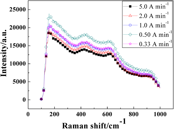
Raman spectra of anodic oxide films on alloy at different VIR
Electrochemical impedance spectroscopy
The Bode plots of samples at different VIR are shown in Fig. 6. The |Z| value, first, increased with decreasing VIR before it reached the maximum at 0··50 A min−1. Thereafter, the |Z| value at VIR = 0··33 A min−1 was approximately the same as that at VIR = 0··5 A min−1 at low frequency. It consisted of two time constants in the selected range of frequency (105–10−2) that were associated with inner and outer layers respectively. The inner layer was compact, and the outer layer was porous, as shown in Fig. 7.
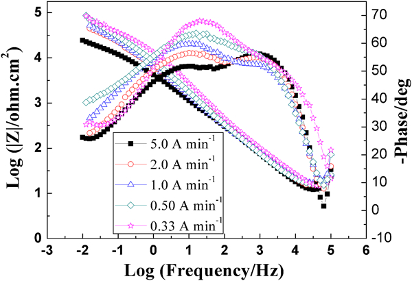
Bode plots of anodic oxide films at different VIR
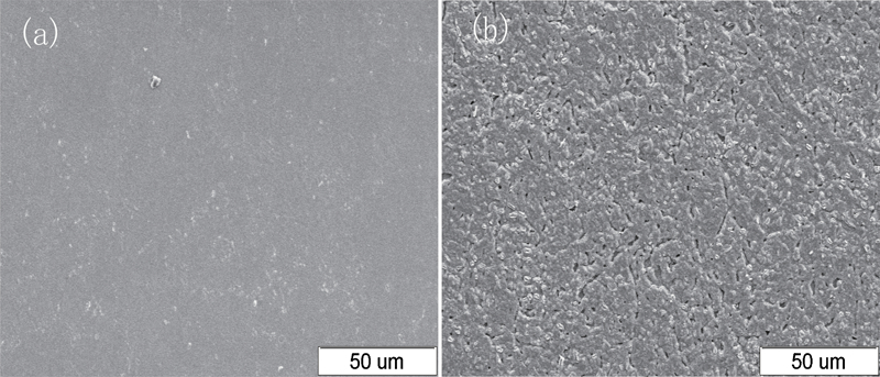
Images (SEM) of a inner and b outer anodised layers
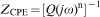
On the basis of these facts, the obtained spectra were interpreted in terms of an ‘equivalent circuit’, as shown in Fig. 8. The depicted model assumes that the oxide film on the titanium alloy comprises a compact inner layer and a porous outer layer (Fig. 7), with RS as the resistance of the solution, RpL as the polarisation resistance of the porous layer, QpL as the capacitance of the porous layer, RbL as the polarisation resistance of the barrier layer, QbL as the capacitance of the barrier layer and W as the warburg impedance. A constant phase element (CPE), representing a shift from the ideal capacitor, was used instead of the capacitance. The impedance of the CPE ZCPE was defined by equation (1) as
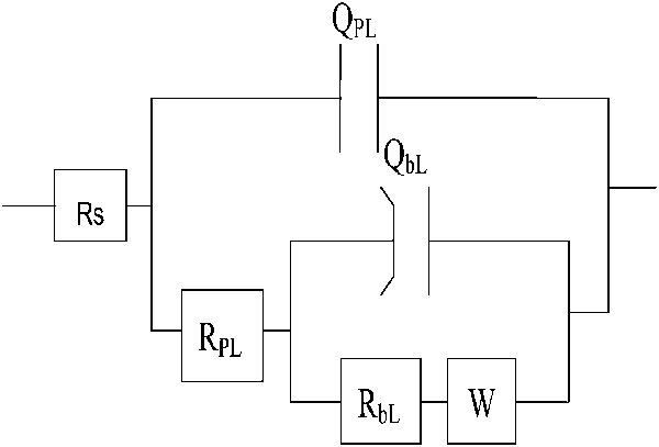
Equivalent circuit diagram for samples at different VIR
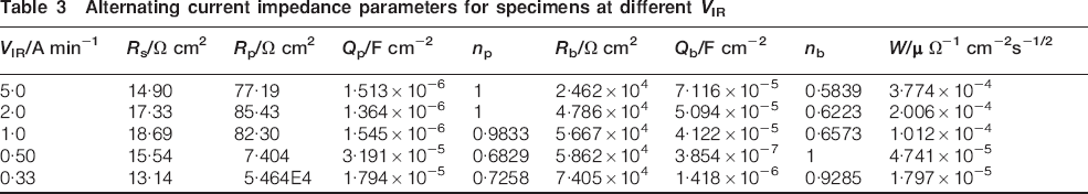
Alternating current impedance parameters for specimens at different VIR
Potentiodynamic polarisation
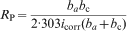
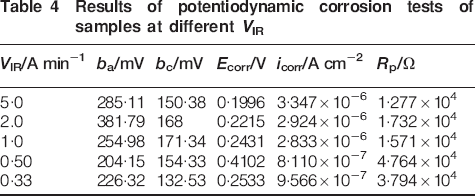
Figure 9 shows the results of experimental potentiodynamic polarisation of samples in a 0··5 mol L−1 H2SO4 solution at different VIR. The corrosion current density icorr, corrosion potential Ecorr and anodic/cathodic Tafel slopes ba and bc were derived from the data obtained. On the basis of the approximate linear polarisation behaviour near the open circuit potential, the polarisation resistance Rp was determined using the Stern–Geary equation14
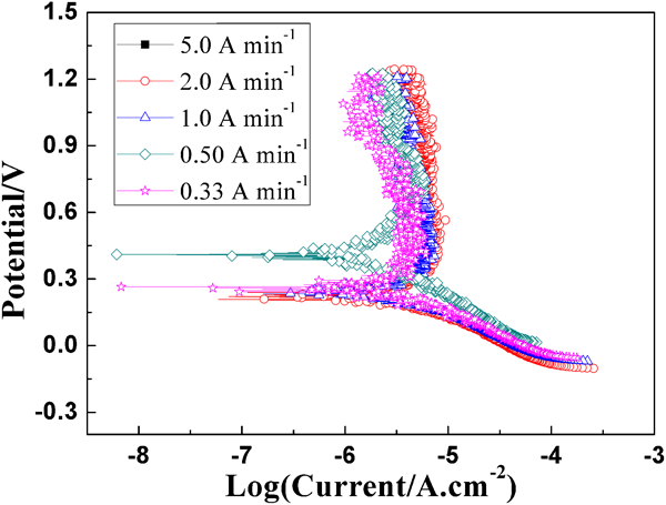
Potentiodynamic polarisation curves of anodic oxide films at different VIR
Results of potentiodynamic corrosion tests of samples at different VIR
Discussion
In general, it is assumed that the behaviour for the growth of anodic oxide film is characterised by the electrochemical dynamics between the ability for the formation of oxide film and the oxide dissolution rate determined by the nature of the electrolyte. The current density increased significantly more rapidly at VIR of 5··0 A min−1 than at 0··33 A min−1. Therefore, when VIR was 5··0 A min−1, the oxide thickness and voltage also increased rapidly. In this situation, the rate of oxide film formation overwhelmingly exceeded the rate of chemical dissolution. As a result, the incremental rate of the voltage in step 1 was much faster at VIR of 5··0 A min−1 (17··7 V min−1) than at VIR of 0··33 A min−1 (3··1 V min−1). This might be associated with the relatively high growth rate that led to the low compactness of the inner layer of oxide film at VIR of 5··0 A min−1 in step 1. In addition, the rate of decline in step 2 was higher at VIR of 5··0 A min−1 (3··8 V min−1) than at VIR of 0··33 A min−1 (0··5 V min−1). The rate of decline in step 2 might be related to the uniformity of the outer layer of the oxide film. In step 3, a dynamic equilibrium between the rate of oxide formation and the rate of chemical dissolution was established. As shown in Table 2, the equilibrium in step 3 was maintained for only 4 min at VIR of 0··33 A min−1 and might be related to the thickness of the outer layer.
The surface roughness, crystal structure and electrochemical impedance of the anodic oxide film were strongly dependent on VIR in terms of the changing rate of the anodising voltage.
The crystal structure of the anodic oxide films can be explained by the ultimate voltage. In general, at low applied voltages, the anodic oxide film is amorphous. With increasing voltages, the structure of the oxide film changes from an amorphous to a crystalline oxide. The ultimate voltage value is maximum at VIR of 0··50 A min−1. The intensity of the peaks corresponds to the ultimate voltage value.
From the EIS results, it can be seen that the solution resistance Rs increased with a decrease in VIR before 1··0 A min−1 and decreased thereafter, which might be associated with the change of the surface state of the anodic oxide films (such as porosity or real surface area). This concurred well with the porosity of the anodic oxide films (Fig. 3). The Rp values are much smaller than the Rb values, indicating that the outer porous layer exhibits a smaller resistance than the inner barrier layer (Table 3); furthermore, the Rb values increase when VIR decreases, indicating that the compact inner layer has a higher ability to protect from corrosion. The lower the incremental rate is in step 1, the higher is the corrosion protection ability of the inner layer before reaching a VIR of 0··50 A min−1.
As VIR decreases, the value of nb increases before VIR = 0··50 A min−1, which indicates that the ‘scattered effect’ of Qbl is weakened and the capacitive interface is strengthened. However, when VIR was 0··33 A min−1, the value of nb decreased, and the capacitive interface was weakened. This was attributed to the fact that the inner layer that formed at VIR of 0··33 A min−1 may be less compact than that formed at VIR of 0··50 A min−1. The compactness of the inner layer increases as VIR decreases before VIR = 0··50 A min−1. This result is consistent with the analysis of the incremental rate in step 1.
In addition, according to Liu,15 the empirical exponent of the CPE is related to the fracture dimension DF of the coarse surface. The change in np is mainly attributable to the roughness of the surface, and DF is a physical variable that corresponds to the roughness. The relation between np and DF is shown in equation (3) as follows16

Furthermore, the electrode is a circle flat with an area of 1 cm2; therefore, there may be a semi-infinite length diffusion step during the process at the electrode. The Warburg impedance decreases when VIR decreases. The diffusing resistance of the reactants is mainly attributed to the inner layer.
Based on the EIS and potentiodynamic polarisation results discussed above, the sample formed at VIR of 0··50 A min−1 has the best corrosion resistance, which could be attributed to the special structure of the inner compact layers and outer porous layers of the anodic oxide films. The special structure of the anodic oxide film could be attributed to the changing rate of anodising voltage at different VIR.
Conclusion
The influence of the incremental rate of anodising current on the structure, surface roughness and electrochemical corrosion of the anodic oxide film on Ti–10V–2Fe–3Al alloy has been investigated in this work, and the following conclusions were obtained.
The relational curves of the anodising voltage and anodising duration at different VIR can be classified into three steps. The surface roughness, crystal structure and behaviour of electrochemical corrosion of the anodic oxide film were remarkably affected by the different VIR with regard to the changing rate of anodising voltage in the three steps of the reaction.
The EIS results and the equivalent circuit analysis have indicated that the base structure of the films consists of a compact inner layer and a porous outer layer, and the structure changed proportionally as VIR decreased. For the inner layer, the lower the incremental rate was in step 1, the higher was the corrosion protection ability maintained in the layer. For the outer layer, the lower the rate of decline in step 2, and the longer the steady time in step 3, the higher the corrosion protection ability maintained.
The uniformity of the surface and the relative intensity of anatase and rutile tended to increase with a decrease in VIR before 0··50 A min−1.
When VIR was 0··50 A min−1, the anodic oxide film was the most uniform, as shown by the least surface roughness, and the amount of crystal phase of the film was the largest. In addition, EIS and potentiodynamic polarisation results have shown that the sample formed at VIR of 0··50 A min−1 had the best corrosion resistance.