
Abstract
In this work, the electrochemical deposition of copper on aligned multi-walled carbon nanotubes (MWCNTs) from an aqueous electrolyte is described. The addition of sodium dodecyl sulphate has been applied to enhance wettability of the hydrophobic MWCNT surface. The transfer of the MWCNT–copper composite film from nickel substrates, as applied for the chemical vapour deposition process for carbon nanotube synthesis, onto adhesive tapes is performed. Moreover, a sandwich layer consisting of copper top layers and copper incorporated MWCNT interlayer was produced. The structure of the resulting composite material of MWCNTs and copper was characterised by scanning electron microscopy. An electrochemical investigation of the MWCNTs on nickel foil and on conductive carbon ribbon by cyclic voltammetry is presented.
Introduction
Carbon nanotubes (CNTs) have been investigated intensively since their discovery and description by Iijima in the early 1990s.1 Iijima used an arc discharge process to form CNTs with various numbers of walls, which were later on named multi-walled CNTs (MWCNTs). Nowadays, a number of formation techniques are described in the literature (see e.g. Ref. 2). Chemical vapour deposition (CVD) is one of the most common methods of producing MWCNTs. Moreover, CVD is suitable for producing MWCNTs on a large scale.3, 4 The deposition of MWCNTs is possible on a number of substrate materials modified by one or more interlayer and catalyst particles. An impressive review of this was written by Dupuis in 2005.2 In view of the application of MWCNTs as future anode material for lithium ion batteries, copper is a preferable substrate. In the early 1990s, Ivanov and co-workers tried to use copper as catalyst material, but in the results, they found only amorphous graphite.5 Hiraoka et al.6 reported that Ag and Cu foils do not support CNT growth. Esconjauregui et al.7 described transition metals with full d-orbitals as being less active since they do not tend to form metal stable carbides, which are crucial for efficient CNT growth. The CNTs or modified CNTs are of great interest in view of the alternative electrode material. The ordered structure, the high conductivity and the high specific surface of aligned MWCNTs are attractive properties for future energy storage material. The combination of aligned MWCNTs with a highly conductive metal is a promising material for future applications in rechargeable lithium ion batteries or electrochemical double layer capacitor.8 – 10 However, the only anodic current collector nowadays is copper foil. Currently used substrates for the deposition of MWCNTs such as nickel are more expensive than copper and/or show lower electric conductivity. Therefore, it seems fundamental to realise MWCNT layers on copper. Consequently, the direct deposition of aligned MWCNTs on copper substrate is still under intensive investigation2, 11 and will be going on. Generally, the investigations are focused on the interlayer between the copper substrate and the formed MWCNTs. The interlayers currently discussed are e.g. titanium with aluminium oxide, pure titanium, pure aluminium oxide or chromium with gold and iron particles as catalysts.12 – 15 Weakly aligned MWCNT on pure copper was formed by the use of ethanol as carbon source in a CVD process at 800°C.16 Concerning the reported problems in depositing aligned MWCNTs on copper foils, the electrochemical deposition of copper on MWCNTs can be a promising alternative method to generate bilayer structures of CNT and copper and might play a key role for anode materials of the next generation. The idea of the authors to generate MWCNTs on copper is a process in the style of replica technique. The formation of aligned MWCNTs takes place on common substrates such as nickel foil, followed by an electrochemical deposition of copper. Finally, the copper/MWCNT bilayer will be removed from the original substrate. In this state of preparation, the bilayer is ready for further processing as an electrode material for novel energy storages (e.g. batteries, electrochemical double layer capacitor). Information about electroless plating of copper or pulse plating of platinum from an aqueous solution on MWCNTs can be found.17, 18 A general problem is the lower wettability between CNT and metal salt solutions.19 Electrodeposition or plating is a well established and widespread technique that is very cost efficient for surface engineering of materials.20 The pulse plating technology has been continuously advanced over the recent time and represents a useful tool to improve the layer properties.21 However, as far as these authors know, the first description of electrochemical deposition of a homogenous and closed copper layer on MWCNTs by pulse plating is in the present work. The method is independent from the substrate that was used for the CVD process. In a final step, the authors deposited copper on top of the copper/MWCNT bilayer and generated a copper/MWCNT/copper sandwich. This sandwich system is primarily a model system that evidences the possibility of additional electrode modification and the versatile possibilities of further electrode processing.
Materials and methods
Chemical vapour deposition process of aligned MWCNTs
The detailed coating procedure is described in a previous published work.22 Nickel foil (50 μm, Alfa Aesar, 99% Ni) was used as substrate for the growth of CNT films. The foil was cut into 4··5×4··5 or 4··5×8 cm pieces and dip coated first with Al2O3 by an Al (iPrO/2,4-pentadionate) precursor developed by Yang et al.23 For the catalyst layer, Fe(2-ethylhexanoate)3 (Alfa Aesar, 50% in mineral spirits) and Co(2-ethyhexanoate)2 (Sigma Aldrich,65% in mineral spirits) in a 40 mol.-%/60 mol.-% ratio were dissolved in 2-propanol (Carl Roth). The catalyst and the buffer layer were deposited by a dip coater (Fraunhofer IWS), and non-homogenous edges (5 cm) were cut off. Carbon nanotube growth by atmospheric pressure CVD was performed with a quartz tube (40 mm diameter) positioned in a split tube furnace (HTM Reetz). The substrate was put into the quartz tube and annealed with 65 K min−1 up to the process temperature of 730°C. Argon at 1··0 slm (standard litre per minute) (5··0, Linde AG) as carrier gas, 0··17 slm ethene (3··5, Linde AG) as carbon precursor and 0··67 slm hydrogen (5··0, Linde AG) were used for the CNT deposition. A small amount of water (85 ppm) enhances the catalyst activity.24 A growth time of 20 min was applied for all samples described in this work.
Electrochemical characterisation
Before the electrochemical experiments, the aligned MWCNTs had to be prepared as a working electrode by the following way. The MWCNT coated foils were placed on a metal sheet covered by a carbon ribbon (Plano GmbH) and fixed with a conductive silver paint (Plano GmbH). A photo resist (H. Schmincke & Co.) or an adhesive tape was used to isolate the metal sheet against the electrolyte (see Fig. 1).
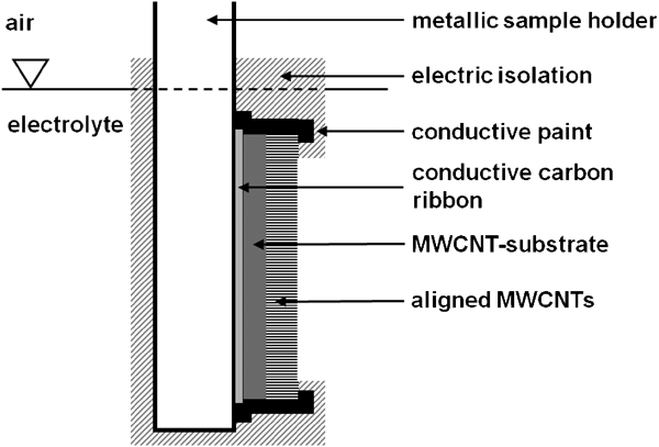
Schematic set-up of MWCNT sample at metallic holder in electrolyte
The surface of the working electrode was ∼0··2 cm2 (the accurate area was always determined before the experiment was started). The electrolytes used for electrochemical characterisation were 0··1M HCl (pH 1··2), 0··1M NaCl (pH 5··5) and 0··1M NaOH (pH 12··4). Owing to the hydrophobic properties of the MWCNT layer, 0··001M sodium dodecyl sulphate (SDS) was added to the electrolytes to improve the wettability. The purity of all the chemicals was pro analyses (p.a.). All electrolytes were purged with nitrogen before the electrochemical experiments and slightly stirred during the measurement. The experiments were carried out in a common cell with a three-electrode design coupled with a computer controlled potentiostat SIMPOT (an in-house development of Heinrich-Heine-Universität Düsseldorf). A saturated Ag/AgCl electrode (Sensortechnik Meinsberg GmbH) was used as reference electrode. A graphite foil (Sigraflex, SGL Group) worked as counter electrode. The potential range used was −1 to +1 V (dE/dt = 100 mV s−1), and all the potentials are given versus saturated Ag/AgCl. Generally, the voltammograms were stable after the second to the fifth cycles. The following diagrams show the tenth cycle of the respective voltammogram.
Electrochemical copper deposition
Figure 2 schematically shows the route to create a copper/MWCNT/copper sandwich. The samples used for the electrochemical copper deposition of MWCNTs on nickel foil were applied as they were received from the CVD process (Fig. 2a and b). The electrolyte consists of 0··2M CuSO4.5H2O, 0··04M H2SO4 and 0··001M SDS (pH 1··6) in deionised water. The addition of SDS improves the wettability of CNTs. After deposition, the samples were cleaned with deionised water and dried in air. In a further step, a carbon ribbon was adhesively bond onto the copper layer (Fig. 2c). Owing to the weak physisorptive bonding of MWCNTs on the nickel foil, the copper/MWCNT bilayer attached to the carbon ribbon can be easily stripped (Fig. 2d). Thereafter, the copper deposition was repeated (Fig. 2e). Finally, the adhesively bond carbon ribbon was removed by tetrahydrofuran (C4H8O), resulting in a copper/MWCNT/copper sandwich (Fig. 2f).
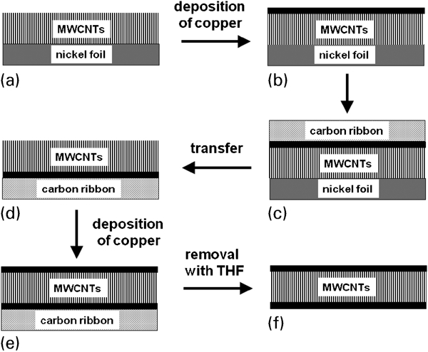
Flow chart of electrochemical deposition process of copper on aligned MWCNTs
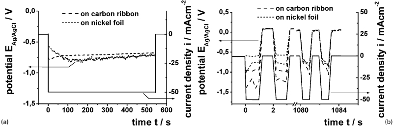
Two different methods were used for the electrochemical deposition of copper. The first method used a continuously electrochemical deposition (dc deposition), as shown in Fig. 3b. The applied current density amounted to i = −50 mA cm−2 during a deposition time of t = 542 s. The second method used a pulse plating process as an alternative way and was carried out with a pulse time ton = 1 s and an off time toff = 1 s (Fig. 3a). The electric charge of the dc deposition as well as of the pulse plating amounts was 27··1 C cm−2 and was kept constant in all experiments.
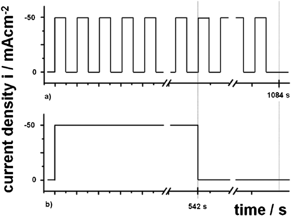
Schematic current–time regime for a pulse plating and b direct plating of copper on MWCNTs
Impedance spectroscopy
Solid state impedance spectroscopy was carried out on a copper/MWCNT/copper sandwich. The sandwich was positioned between two planar platinum disks. The experiments were carried out in a two-electrode design coupled with a computer controlled potentiostat Reference 3000 (Gamry). The dc voltage was 0 V, and the amplitude of the super positioned ac voltage was 1 mV in a frequency range of 105–10−1 Hz.
Results and discussion
Electrochemical characterisations
Figure 4 shows the cyclic voltammograms on both MWCNTs on nickel (Fig. 4a) and on carbon ribbon as substrate (Fig. 4b) in various electrolytes (0··1M HCl, 0··1M NaCl and 0··1M NaOH). The addition of surfactants improves the wettability of hydrophobic MWCNTs. The difference between both diagrams is evident. The voltammograms shown in Fig. 4a are mainly characterised by the electrochemical dissolution of nickel. Nickel passive layers are highly resistant against alkaline solution (e.g. NaOH and KOH).25 The passive layer is electron conductive, and the rise of current density at higher potentials is caused by oxygen evolution. Nickel forms passive layers also in acidic as well as in neutral solutions. Therefore, the necessary passivation current density increases with decreasing pH value (from 0··1 μA cm−2 at pH 11··7 to 70 mA cm−2 at pH 0··3).26 Furthermore, in the presence of chloride ions, nickel tends to cause pitting corrosion, which additionally limits the potential range of passivity.
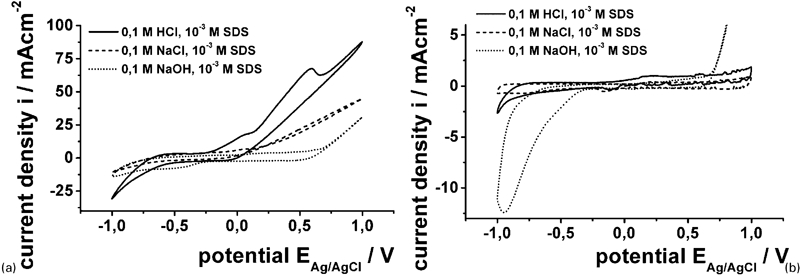
Cyclic voltammetry of MWCNTs on a nickel foil and b conductive carbon ribbon at various electrolytes with scan rate of 100 mV s−1
In contrast, Fig. 4b only shows the charging and recharging of the electrochemical double layer on the MWCNT. No oxygen evolution can be observed in either of the chloride containing electrolytes. In sodium hydroxide solution, the oxygen evolution can be expected at 0··3 V; however, the reaction does not begin before 0··7 V. On the cathodic side, the hydrogen evolution should start depending on the pH value of the electrolyte (theoretical values: 0··1M HCl: EH2 = −0··27 V; 0··1M NaCl: EH2 = −0··58 V; 0··1M NaOH: EH2 = −0··93 V). Additionally, the overvoltage of hydrogen reduction on carbon strongly depends on the carbon modification and varies in the literature between 0··3 and 1 V (for = 1 mA cm−2).27 In fact, the hydrogen evolution is not really observable in these experiments. In view of the aforementioned theoretical values, the increasing current density in the alkaline solution at −0··3 V cannot be hydrogen evolution. A possible hypothesis might be the reduction of functional groups (e.g. carbon acid groups).28 Functional groups of MWCNTs are likewise caused by the manufacturing process and are generated on defects or impurities (e.g. nanocrystal metal catalysts, amorphous carbon and carbon nanoparticles).29 – 31 The estimated double layer capacitance of MWCNTs in all electrolytes is ∼2 mF cm−2. That means that if a double layer capacitance of 25 μF cm−2 is assumed, the specific surface is 84-fold higher than the geometric surface of the samples (8··4 m2 g−1).
Furthermore, nickel corrosion (shown in Fig. 4a) is a sign for the complete wettability of hydrophobic MWCNTs. Otherwise, the hydrophobic properties would inhibit the penetration of aqueous solutions between CNTs all the way down to the substrate. The wettability is the requirement for a successful electrochemical deposition of copper from aqueous electrolytes. In distilled water without any wetting agent, an air film is observed between the aligned MWCNT array and the electrolyte.
Electrochemical deposition of copper
The copper deposition from acidic sulphate solution is well known and can be described according to equation (1)

Potential during deposition process with a static and b pulse regime; for pulse regime two selected examples are presented for every sample
Figure 5b shows that the initially required overvoltage to realise the applied current density is clearly distinguished. However, the overvoltages converge at the end of the experiment. Unfortunately, the differences cannot be correlated with the substrate material. Moreover, the producing and experimental conditions of all the experiments were exactly the same. A change in the concentration of metal ions inside the electrolyte can be neglected. An interesting fact of the overvoltage development is shown at higher number of pulses (Fig. 5b). During the pulse time ton, the overvoltage increases. A depletion of copper ions in the part of the electrolyte that is deeply penetrated into the MWCNT layer is assumed.
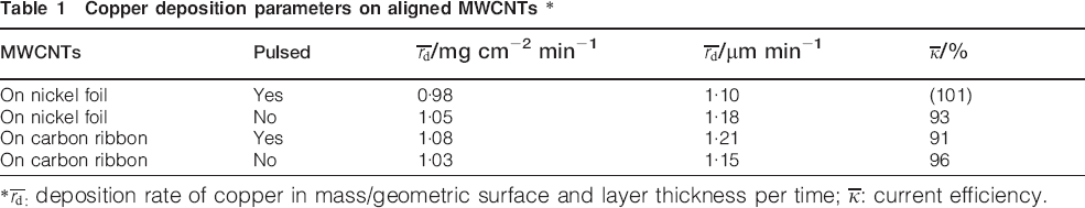
An overview of the results of the copper deposition process is shown in Table 1. The intended copper layer thickness was 10 μm. The current efficiency is determined by gravimetric measurements. With respect to the very low deposited mass (∼7 mg/sample) and accuracy of the balance (0··1 mg), the current efficiency amounts to more than 90%. The high current efficiency indicates no significant side reactions. The layer growth rate is approximately 1··1–1··2 μm min−1. The difference between dc plating and pulse plating are negligible.
Copper deposition parameters on aligned MWCNTs *
 /mg cm−2 min−1
 /μm min−1
 /%
/% : deposition rate of copper in mass/geometric surface and layer thickness per time;
 : current efficiency.
Electron microscopy
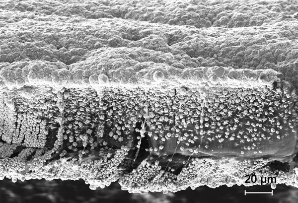
Figure 6 shows a cross-section of a copper deposited MWCNT layer. It can be easily distinguished among the thin aluminium oxide layer (Fig. 6d), the MWCNT layer with individual copper particles (Fig. 6c) and the closed copper layer on top of the MWCNTs (Fig. 6b).
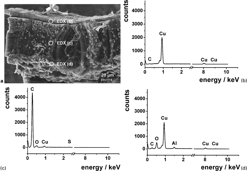
a field emission SEM cross-section of copper/MWCNT sample prepared by copper deposition with pulse plating on aligned MWCNT-nickel foil and b, c, d EDX spectra at tagged measurement points
The white circles in Fig. 6a correspond to the EDX spectra shown in Fig. 6b. The EDX spectra confirm the aforementioned description of the various ranges of the complete layer. The fact that copper was found in all regions of the layer shows evidence of the penetration of the complete porous volume by the copper electrolyte. Figure 7 shows a detailed investigation of the copper/MWCNT bilayer. The copper layer is clearly visible as a small bright line in Fig. 7a. It is evident that the amount of copper deposition decreases with increasing penetration depth. Copper forms a closed deposition layer. Close to the interface copper/MWCNT, the covering with copper is still high (Fig. 7c). In contrast, deep in the MWCNT layer, only single copper particles or small copper clusters can be found (Fig. 7d). Moreover, the particle size seems to be smaller deep inside the MWCNT layer than close to the interface. This can be explained by the depletion of the copper electrolyte during the electrolytic deposition deep inside the MWCNT layer. The longer diffusion way limits the replenishment of copper ions from the bulk electrolyte. Figure 7c additionally shows a small number of slightly agglomerated nanotubes (marked by white arrows).
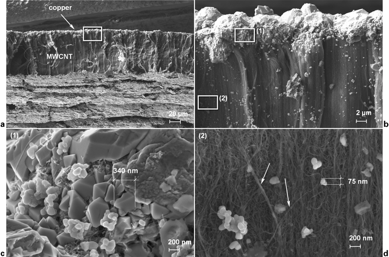
Field emission SEM of copper/MWCNT bilayer
The development of copper deposition and layer formation during the experiments is schematically shown in Fig. 8. If the copper layer on top is closed, a further deposition of copper deep inside the MWCNT layer is excluded (state III). The preferred deposition on the top is caused by the penetration kinetic of the electrolyte into the intermediate spaces of the MWCNTs, which is determined by the diffusion and wettability. A slight agglomeration of the tubes is observed, but the destruction of the homogenously aligned structure is prevented through the fixation of the tube tips by the deposited copper layer (Fig. 7).
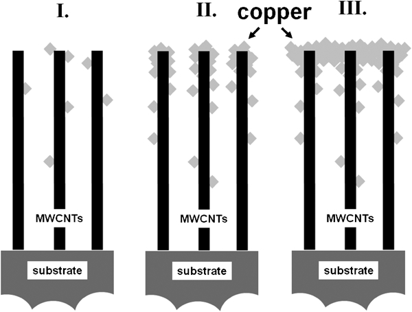
Possible scheme for self-limiting copper deposition inside MWCNT layer
Figures 9 and 10 show the morphology of the deposited copper layer produced with pulse plating and dc plating respectively. It is obvious that the surface roughness of the pulse plated copper layer is smaller in comparison to the dc plated copper layer. Furthermore, the pulse plated copper layer is completely closed. In contrast, the dc pulsed layer shows a number of small cracks or fissures (marked by white arrows in Fig. 10a). Detail images of both copper layers with higher magnification are shown in Figs. 9b and 10b. The pulse plated layer is very smooth, and only a number of individual single crystals with a double pyramidal habitus are visible. In Fig. 10b, such individual particles are also visible. However, the particle size is higher in comparison to Fig. 9b, and the crystallites tend to agglomerate.
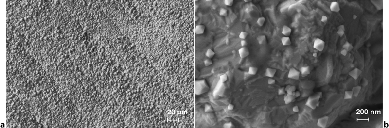
Morphology of copper layer by pulse plating
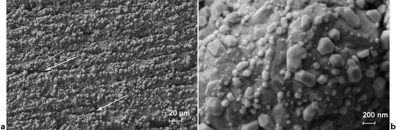
Morphology of copper layer by dc plating
Figure 11 shows a complete copper/MWCNT/copper sandwich that is plated on both sides. The procedure of double side process is already described schematically in Fig. 2.
Nearly homogenous aligned MWCNT on deposited copper by deposition way via adhesive carbon tape, two sided deposited ‘sandwich’
Such sandwich structures as shown in Fig. 11 possess a very low electric resistance. The contact resistance of the sandwich was measured using impedance spectroscopy. A sample that was cut into squares of 0··39 cm2 was used. The sample thickness amounts to 100 μm. The measured resistance at 0··1 Hz amounts to 0··109 Ω. Based on these data, the specific resistance was calculated to 0··413 Ω m.
Conclusion
The present work evidences the feasibility of the electrochemical deposition of copper on aligned MWCNTs. For the first time, the authors developed a procedure that allows the production of free standing copper MWCNT sandwich layers based on a combination of replica technique and pulse plating. The pulse plating technique and the application of wetting agents like SDS have proven to be useful and necessary to form a closed copper deposition and a homogenous copper layer on top of the MWCNT layers. Individual particles in the intermediated spaces of MWCNTs are generated by self-limiting deposition. As a result, the formation of a sandwich layer with ∼100 μm thickness of aligned MWCNT layer between two nearly 10 μm thickness copper layers is shown.
Footnotes
Acknowledgements
The authors wish to thank the European Union and the Free State of Saxony for the financial funds of this project (grant no. 13858/2379).