
Abstract
ZnO thin films were deposited onto glass substrates using sol–gel spin coating technique from starting solutions having different precursor concentrations (0·1, 0·3 and 0·5M). The effects of precursor concentration and annealing temperature on the physical properties of the films were investigated. The X-ray diffraction studies confirm that all the films have preferential orientation along the (002) plane with hexagonal wurtzite structure. The optical transparency gradually decreases (from 95 to 80%) as the precursor concentration increases. The optical energy gap is in the range of 3·18–3·32 eV. The systematic study shows that the post-annealing process has significant impact on the quality of the films. The SEM images depict that the grain size decreases as the precursor concentration increases, and the AFM images show that the film annealed at 550°C has well defined uniform grains. The lowest dislocation density is observed for 0·3M annealed at 550°C.
Introduction
Increasing attention is being paid for improving transparent conductive materials suitable for a large variety of optoelectronic devices, defrost windows, flat panel displays, touch screens and electrochromic devices.1, 2 A large number of transparent conducting oxides (TCOs) such as tin oxide, indium oxide, cadmium oxide, titanium dioxide and zinc oxide have been widely studied for conventional transparent electrode applications.3 – 11 Among these, zinc oxide has become a subject of increasing interest owing to its attractive physical properties, such as high electrical conductivity and visible (Vis) transmittance together with its high reflectance in the IR region. Its abundance in nature and non-toxicity make it an attractive candidate for TCO applications when compared with other TCO materials.12 The inexpensive zinc oxide has a direct wide band gap of 3·37 eV and a large exciton binding energy of 60 eV, much larger than other semiconductor materials, making it a focussing material for advanced applications such as window layer in heterojunction solar cells, heat mirrors, multilayer photothermal conversion systems, solid state gas sensors, dye sensitised solar cells, etc.13 – 15
ZnO thin films can be realised using different fabrication methods, including physical vapour deposition,16 chemical vapour deposition (CVD)17 and wet solution processing approaches, such as sol–gel processes.18 The structural, electronic transport and optical properties of ZnO films are very sensitive to the preparation method and deposition conditions. Earlier researches have shown that ZnO thin films with high quality were mostly realised with vapour phase growth techniques, such as molecular beam epitaxy,19 metal–organic CVD20 and sputtering deposition.21 Nevertheless, due to the sophisticated equipment set-up, these techniques are expensive. Some other alternative fabrication techniques, which offer advantages in terms of the manufacturing cost, have been explored recently. For example, ZnO can be fabricated using low cost wet processing approaches such as electrochemical, chemical bath and sol–gel spin coating techniques. The sol–gel spin coating process provides a simplified fabrication route for the ZnO layers as it eliminates the need of vapour phase deposition equipment. This technique is particularly suitable to produce ZnO colloids and films in a simple, cost effective and highly controlled way. The chemical composition can be controlled with relative ease, and large area fabrication of the thin films can be achieved using this technique.22, 23 There are relatively few reports on the sol–gel spin coating preparation of ZnO thin films. In the present work, a low cost sol–gel spin coating technique is used to synthesise ZnO films. The influence of precursor concentration and post-annealing on the material properties of ZnO thin films was investigated.
Experimental
ZnO thin films were deposited by sol–gel spin coating method onto glass substrates. Zinc acetate dihydrate, ethyl alcohol and diethanolamine were used as starting material, solvent and stabiliser respectively. The concentration of the zinc acetate was kept as 0·1, 0·3 and 0·5 M. The resultant solution was continuously stirred at 50°C for 2 h. The precursor solution was then filtered and finally aged for 24 h at room temperature in order to yield a clear and homogenous aqueous solution. The ZnO films were spin coated onto glass substrates, keeping the spinner speed as 2500 rev min−1 for 30 s. The deposited wet film was heated at 100°C for 15 min and allowed to cool for 10 min at room temperature. The deposition process was repeated to obtain the workable thickness of the film. To study the effect of annealing on the structural and optical properties, the obtained multilayer films were post-annealed for 1 h at various temperatures, namely, 300, 400, 500, 550 and 600°C. The thicknesses of the films were in the range of 800 nm.
Surface analysis was carried out using scanning electron microscope (Hitachi S-3000 H) and atomic force microscope (Veeco-di CPII). The X-ray diffraction patterns and optical transmittance spectra were recorded using an X-ray diffractometer (PANalytical-PW 340/60 Xpert PRO) and UV–Vis–near IR spectrophotometer (PerkinElmer Lambda 35 model) respectively.
Results and discussion
Surface morphology
Even though some voids are seen in the SEM images (Fig. 1), the surfaces of the films appear to have good packing density with spherical grains. The packing density increases with the increase in molar concentration of the solution. The grain size is found to decrease as the precursor concentration increases, which in turn causes the decrease in Vis transmittance, as discussed in the optical studies.
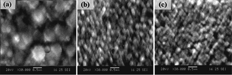
Images (SEM) of annealed (550°C) ZnO films deposited from starting solutions having precursor concentrations:
The X-ray diffraction studies (discussed in the next section) showed that the crystallite size initially increases with the increase in precursor concentration. The crystallite size is 80 nm for the precursor concentration of 0·1M, and the value increases to 89 nm for the precursor concentration of 0·3M. At the same time, the SEM images depict that the grain size value decreases as the precursor concentration increases. Actually, these two physical quantities, viz., crystallite size and grain size, obtained from the X-ray diffraction profiles and the SEM images respectively are not indicating the same entity. The above mentioned point can be clearly understood from the reports of Yunos et al.24 and Muruganantham et al.2
According to Muruganantham et al.2, crystallites are the ‘coherently diffracting domains’ of crystals and grains may contain several of these domains. When we deform a single crystal, several subgrains having different orientations are formed. Then, each and every subgrain will be considered a crystallite. As a special case, if a grain is made up of a single crystallite, then only the grain size and the crystallite size have the same value. Hence, we can say that the granule morphology is not representing the real crystallite size.
The AFM images of the ZnO films deposited from precursor concentration 0·3M annealed at temperatures 300, 400, 500, 550 and 600°C are presented in Fig. 2. When the film is annealed at 300°C, the grains are not formed well as seen in Fig. 2a. However, the increase in annealing temperature gradually improves the formation of grains (Fig. 2b and c), and very well defined grains with uniform packing density are observed in the case of 550°C (Fig. 2d). A further increase in annealing temperature (600°C) slightly disturbs the uniformity of the surface of the film (Fig. 2e). From the AFM images, we can conclude that the annealing temperature causes a significant impact on the surface morphology of the sol–gel spin coated ZnO films.
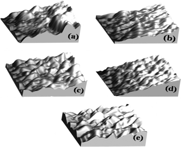
Images (AFM) of ZnO films deposited from precursor concentration of 0·3M annealed at temperatures a 300°C, b 400°C, c 500°C, d 550°C and e 600°C
Effect of precursor concentration on structural properties
The X-ray diffraction patterns of ZnO thin films prepared using precursor concentrations of 0·1, 0·3 and 0·5 M, post-annealed at 550°C for 1 h, are shown in Fig. 3. These patterns show sharp and narrow diffraction peaks indicating that the materials generally exhibit good crystallinity.
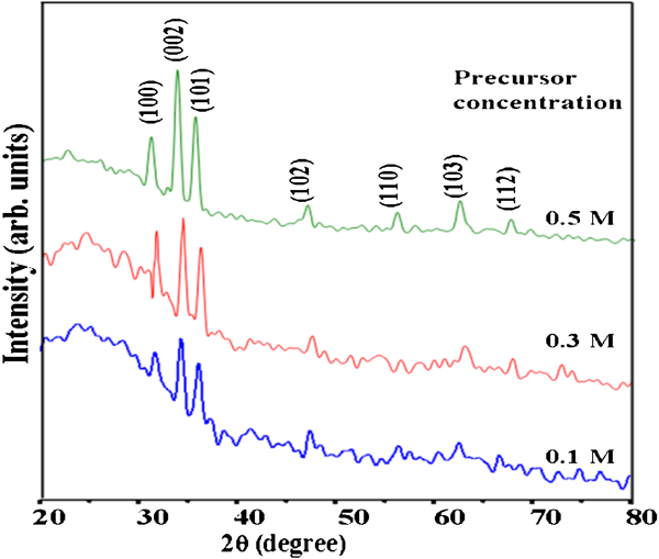
X-ray diffraction patterns of ZnO films deposited starting solutions having different precursor concentrations annealed at 550°C
The X-ray diffraction profiles reveal that the deposited films have polycrystalline nature with hexagonal würtzite structure. All the films have preferential orientation along the (002) plane with the c axis perpendicular to the substrate surface irrespective of the precursor concentration. However, the intensity of the (002) peak progressively increases with the increase in precursor concentration, which may be attributed to the gradual increase in thickness of the film that causes more reflections along the increased number of (002) planes. This (002) orientation is especially important for piezoelectric applications.25 The other prominent peaks seen are corresponding to planes (100), (101), (102), (110), (103) and (112) according to the JCPDS card no. 36-1451. The variation in the value of full width at half maximum clearly shows that the degree of crystallinity is strongly influenced by the concentration of the precursor. The crystallite sizes ‘D’ of ZnO films were determined using Debye Sherrer's formula26 D = 0·94λ/β cos θ, where λ is the applied X-ray wavelength (0·154056 nm for Cu Kα ), β is the full width at half maximum and ‘θ’ is the Bragg angle. The calculated crystallite sizes of the ZnO films are given in Table 1, and the values imply that the increase in precursor concentration from 0·1 to 0·3 M results in a larger crystallite size. This may be due to the tendency of high agglomeration among smaller crystallites to form larger crystallites, which is noted in thin films with increased precursor concentration. When the amount of solute is increased in the sol, the electrostatic interaction between the solute particles becomes larger, thus increasing the probability of more solute to be gathered together to form a larger crystallite. Therefore, with the increase in precursor concentration, the crystallite size increases. The observations of Durgajanani et al.27 during their study on the influence of precursor concentration on the structural properties of spray deposited ZnO thin films are supporting evidences for this discussion. Moreover, at a lower precursor concentration (0·1M), the nucleation rate is relatively low, which leads to a small crystallite size of 80·3 nm. On increasing the precursor concentration to 0·5M, a smaller crystallite size of 77·1 nm is obtained. This may be ascribed to the degradation of crystallites instead of the agglomeration. It could be pointed out that continuously increasing the precursor concentration may not necessarily result in a higher crystallite size. From these observations, we can say that when the precursor concentration exceeds a certain level (0·3M in the present study), the reaction proceeds very fast, resulting in a hindrance to the growth of ZnO crystals with regular morphology. A report on the effect of precursor concentration on the growth mechanism of the doped ZnO films by Rodriguez-Baez et al.28 supports this argument. They reported that when the film grows faster, there is no chance of rearrangement of the material into a more definite structure. Generally, when the concentration of the precursor increases, the deposited ZnO films include the effects of increasing Zn incorporation, increasing growth rate as well as reorientational effects. 29 29,30
Structural and optical parameters of ZnO films prepared from different precursor concentrations (D: crystallite size; Δ: dislocation density; a, c: lattice constants; L: bond length; Eg: band gap; ϵzz: residual stress)
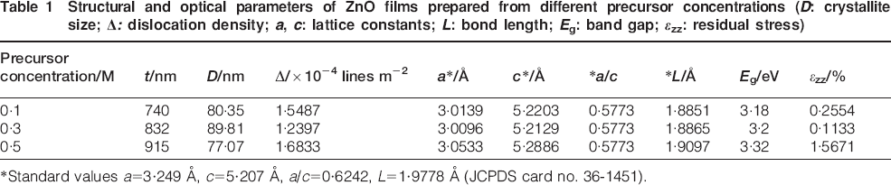
Standard values a = 3·249 Å, c = 5·207 Å, a/c = 0·6242, L = 1·9778 Å (JCPDS card no. 36-1451).
The dislocation density δ that represents the amount of defects in the film is determined 31 31,32 from the formula δ = 1/D2 (Table 1). The dislocation density initially decreases on increasing the concentration from 0·1 to 0·3 M and then increases for further increase in concentration, suggesting that the precursor concentration of 0·3M is suitable for fabricating ZnO films with lesser lattice imperfections. The lattice constants ‘a’ and ‘c’ of the wurtzite structure of ZnO are calculated using the well known analytical method33 by employing the relations a = (⅓)1/2(λ/sin θ) and c = λ/sin θ. The calculated values of a, c and a/c are also given in Table 1. A comparison of the observed a/c values with the standard values34 indicates an agreement to a good extent. The slight reduction observed in the ‘a’ and a/c values may be attributed to the oxygen vacancies and the interstitial Zn atoms incorporated in the ZnO lattice. The Zn–O bond length L is given by35 L = {a2/3+(½−u)2 c2}1/2, where the u parameter in wurtzite structure is given by u = a2/3c2+0·25.
The ZnO bond length increases (Table 1) with the precursor concentration, and there is good agreement between the JCPDS standard data and the observed value of the Zn–O bond length of ZnO film prepared with the precursor concentration 0·5M. When the precursor concentration increases from 0·1 to 0·5 M, the peak positions of preferred orientation (002) are shifted to lower 2θ values, which leads to the increase in d value and hence the bond length. This may be due to the presence of a large number of interstitial Zn atoms in the ZnO lattice. This is further confirmed by the increased dislocation density, resulting in the increase in precursor concentrations, as seen in Table 1.
The strain along the c axis ϵzz is given by the relation36
From the diffraction patterns, it is also observed that there was no peak due to impurities, indicating that high purity ZnO thin films have been achieved in the present study by the sol–gel spin coating method.
Effect of post-annealing temperature on structural properties
The X-ray diffraction spectra and structural parameters of ZnO thin films prepared using precursor concentration 0·3M and post-annealed at various temperatures are shown in Fig. 4 and Table 2 respectively. From the figure, it is observed that the preferential growth is along the (002) plane for all the films irrespective of the annealing temperature. It is obvious from Fig. 4 that the intensity of the (002) peak progressively increases up to 550°C and decreases suddenly for the further increase in temperature. This may be due to the decrease in the thickness of the film caused by the evaporation of ZnO at certain higher temperature.39 This result implies that the crystalline quality of the film strongly depends on the annealing temperature. From these results, we can conclude that 550°C is the suitable annealing temperature for obtaining good quality sol–gel spin coated ZnO films.
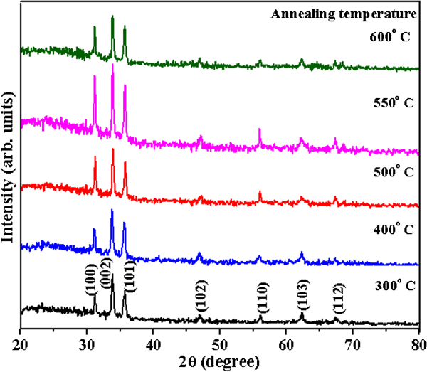
X-ray diffraction patterns of ZnO films deposited from precursor concentration 0·3M from annealed at different temperatures
Structural parameters of ZnO films deposited from starting solution with concentration 0·3 M
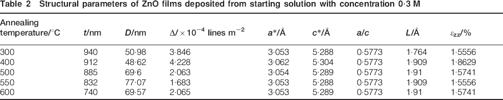
The ϵzz values obtained for the annealed films are summarised in Table 2. From the values, it is obvious that the annealing temperature hardly influences the tensile residual stress of the ZnO films.
Optical properties
Ultraviolet–Vis–near IR transmission and photoluminescence studies
Figure 5 shows the optical transmittance spectra of the ZnO films in the wavelength range of 300–1000 nm. The film transmittance decreases with the increase in precursor concentration.27 Chinnappa et al.40 reported similar results for fluorine doped tin oxide films. For the film prepared with 0·1M concentration, the optical transmittance is 95%, whereas for the films of 0·3 and 0·5 M precursor concentrations, it is only 90 and 80% respectively. This reduction in transmittance at high molar concentrations is due to the higher thickness of the films and the optical scattering at the increased number of grain boundaries. It is worth mentioning here that in transparent metal oxides, the metal/oxygen ratio decides the percentage of optical transmittance, and a metal rich film usually exhibits less transparency.41 Moreover, the optical transmittance of the film is known to strongly depend on the grain size of the films. The higher transmittance at lesser concentration may be attributed to the larger grain size. When the grain size increases, the grain boundary scattering reduces, which causes an improvement in transmittance. The SEM (Fig. 1) results act as supporting evidence for the above discussion. From the SEM images, it is found that the grain size decreases as the precursor concentration increases. The decrease in grain size causes an increase in the grain boundary density of the film.
Transmission spectra of ZnO films annealed at 550°C deposited from starting solutions having different precursor concentrations
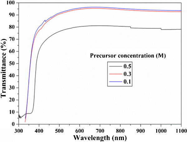
The transmittance of the films prepared from starting solutions having concentration 0·3M as a function of annealing temperature is given in Fig. 6. The transmittance is nearly 60% for the as deposited film, and the value increases gradually to 95% as the annealing temperature increases. This increase in transmittance may be attributed to the reduction in the thickness of the film caused by the evaporation of ZnO at higher annealing temperature. Tasi et al.39 observed that the thickness of the film becomes 10% thinner after being annealed at 500°C. In the present study also, it is noticed that the thickness of the film is gradually reduced due to annealing, as given in Table 2.
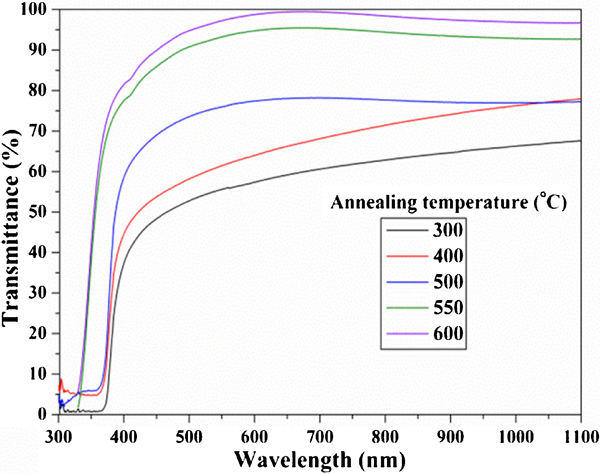
Transmission spectra of ZnO film precursor concentration of 0·3M annealed precursor concentration of 0·3M annealed
Absorption owing to an interband transition of ZnO occurs in the wavelength range of 340–380 nm. The optical energy gap Eg and the absorption coefficient α are related by the equation a = (A/hv)(hv−Eg) β , where A is a constant, hv is the incident photon energy and β is the number that characterises the nature of electronic transition between valance and conduction bands. For direct allowed transition, β = (1/2), and it is known that ZnO is a direct band gap semiconductor.20
The plot representing the variation of (hvα)2 versus hv, obtained using the above equation, is known as Tauc's plot.20 The band gap energy of the grown ZnO films are determined by the extrapolation of the linear part of Tauc's plot (not shown). The obtained optical band gap values are summarised in Table 1. As the precursor concentration is increased from 0·1 to 0·5 M, the optical band gap is blue shifted from 3·18 to 3·32 eV. Similar observations have been made by Tan et al.35 for ZnO thin films grown by metal–organic CVD. Therefore, it may be said that an increase in precursor concentration widens the optical band gap. This band gap broadening can be related to the Moss–Burstein effect. The Moss–Burstein effect is associated with the lifting of the Fermi level into the conduction band of degenerate semiconductors, which leads to the broadening of the band gap (blue shift).
Conclusion
Highly transparent and crystalline ZnO thin films were fabricated using a simple sol–gel technique. From the structural studies, it is observed that all the films were grown along the (002) plane with c axis perpendicular to the surface of the substrate irrespective of the precursor concentration and annealing temperature. The optical transmittance at 550 nm is the highest (95%) for the film deposited with 0·3M precursor concentration, which is sufficient for making the best solar cell devices. Appreciable crystalline quality and good stoichiometric nature were observed for ZnO films coated using the precursor concentration of 0·3M, annealed at 550°C.
Footnotes
Acknowledgements
The authors are thankful to Dr P. Manisankar, Professor and Head, Department of Industrial chemistry, Alagappa University, Karaikudi, Tamil Nadu, India, for AFM measurements.