
Abstract
In an effort to produce more cost effective diamond to metal interfaces, mono- and polycrystalline diamond powders were coated with nickel alloys using electroless chemical deposition techniques. Ni–P and Ni–B coatings were deposited using an acidic and an alkaline solution respectively. These deposition procedures were preceded by a thermal surface functionalisation step and a sensitisation step using a Pd–Sn colloidal solution. Imaging by SEM and chemical analyses show uniform coverage of the coating, independent of diamond's crystalline planes, and having thicknesses consistently <200 nm.
Introduction
The chemical and physical properties of diamond make it one of the most challenging materials to sinter into a monolithic solid from powder form; growth of thick substrates can only be achieved through chemical vapour deposition. Its rigid structure and high C to C bond strengths makes diamond very appealing for many applications, thermal management in particular. Diamonds possess one of the highest thermal conductivities (TCs) while having the lowest coefficient of thermal expansion among most materials, which give them high potential to be used for heat sink and heat spreading applications in electronic components.
Diamond metal matrix composites (MMCs) combine the thermal properties of diamonds with the ease of consolidation of most engineering metals (e.g. copper and aluminium) to yield a material whose TC and coefficient of thermal expansion values are dependent on the percentage content of diamond. However, to achieve these properties, the diamonds must first adhere well with the metal matrix in order to obtain good transport of phonons.1
Production of an interface is of critical importance for diamond MMCs, as it serves to bond the diamond phase to the matrix by the formation of a carbide layer. Magnetic sputtering and other physical techniques are reported to deposit interfaces containing Mo, Cr, Ti, B, W and others.2 – 6 Electroless plating techniques have been investigated7 – 9 to a lesser extent since the choice of metal being deposited is limited. An important aspect of such interfaces is that they must be sufficiently thin so that the transport of phonons is not disrupted since the mentioned elements do not possess very high TC. Most of the cited studies made use of interfaces being thicker than 1 μm, while the others produce thicknesses being lower, which always led to diamond MMCs having the highest TC.
This paper reports the deposition of nanometric thick interfaces on to diamond particles using two electroless plating techniques. Pretreatment of the particles was necessary to obtain good quality and adhesion of the interface to the substrate surface. Scanning electron microscopy (SEM), energy dispersive spectroscopy (EDS) and chemical analyses were used to determine the morphology and composition of the as deposited interfaces.
Experimental
Pretreatment
Diamond grits (element 6) having diameters 213, 91 and 31 μm were used in this study; the first two are monocrystalline, while the 31 μm grit had polycrystalline morphology. The samples were heated in air to 350°C for 15 min in an electric oven in order to functionalise the surface. The grits were then sensitised using POP Activator (IWG GmbH) one step solution, which consists of a Pd–Sn colloidal solution. The activated grit was then treated using IWG POP Accelerator solution to enhance the reactivity of the surface.
Deposition of Ni alloy interface
The diamond grit was immediately placed in the reaction solutions (given in Table 1 Tables 1 and 2) following the pretreatment. Plating time was 5 min, and the temperature of both solutions was kept at 90°C. After plating, the grits were thoroughly rinsed with deionised water and dried in a vacuum desiccator for 12 h.
Chemical composition of electroless Ni–P solution11
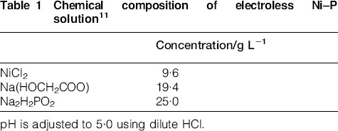
pH is adjusted to 5·0 using dilute HCl.
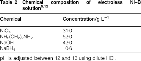
pH is adjusted between 12 and 13 using dilute HCl.
Characterisation
Characterisation was performed using a Carl Zeiss Merlin SEM equipped with a Gemini II electron gun and an Amatex EDAX detector for EDS analysis. All images were taken using backscatter mode at various acceleration potentials to minimise charging.
Atomic absorption spectrophotometry (Perkin-Elmer 2380) was used to measure the amount of Ni present in the coated diamonds following digestion using 50% concentrated nitric acid. This was used to estimate the thickness of the coating.
Results and discussion
Pretreatment
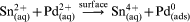
Functionalisation of the diamond grit surface occurs by partial oxidation of the carbon atoms found at the surface. Such treatment allows the formation of carbonyl groups, which would then allow better adsorption of Sn2+ and Pd2+ ions. Proper functionalisation led to uniform surface coverage of the deposit as the surface would be wholly activated.
Pd2+ ions adsorbed onto the diamond surface are reduced into the Pd0 particulates by Sn2+ ions, which then serve as catalytic initiators for the electroless reaction. The overall reaction is as follows
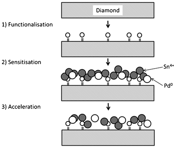
Schematic representation of pretreatments
Deposition of interfaces
Deposition of Ni–P and Ni–B layers is initiated by the adsorbed Pd0 sites, which lead to the reduction of Ni and the reducing agents to produce the appropriate alloys. The mechanisms for the reduction in hypophosphite and borohydride anions can be found in Refs. 11, 13 and 14. The codeposition of either P or B in the interface depends strongly on the bath composition and can therefore be tuned to ones’ needs. The concentrations of P and B were chosen to be as small as possible to reduce the formation of intermetallics during any sintering process, which could then influence the wetting properties between the diamond and the metal matrix phases. Measurements (EDS) showed that an average P composition by 7·09 mass-% was obtained for the Ni–P coatings, while the B content could not be measured.
As seen in Fig. 2a and b, the diamonds were uniformly covered with both solutions. Even polycrystalline diamond grit was noted to be fully coated; hence, this shows that the electroless process is suitable to build interface layers onto the diamond particles even if the surface is highly irregular. The nuclei, which can be observed in Fig. 2a, arise from the rate of deposition of the solutions. The higher the plating rate, the less time such nuclei have to grow laterally, thus grow in size to form globules. Such globules can pose adhesion problems with the metal matrix, as they could be loosely attached to the interfacial film. The Ni–B appears to be smoother since its plating rate is much slower than that of Ni–P.11
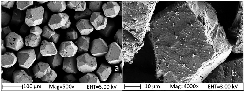
Images (SEM) of a monocrystalline Ni–P coated and b polycrystalline Ni–B coated diamond particles
Thickness evaluation
The thickness of the interface was estimated using both atomic absorption spectroscopy (AAS) and SEM imaging. The AAS measurements produced an average thickness value of 107±34 nm. This value is more holistic than SEM measurements since the deposit was dissolved and the Ni content was evaluated. By converting the mass of the dissolved Ni into its equivalent volume and by working out the total surface area of the digested sample, the thickness of the interface was worked out. However, calculations for such measurements have been oversimplified, for example the density of the interface will vary depending on the P or B content and also due to the porosity of the deposited alloy. Moreover, the particles have been assumed to be spherical and used their effective diameter to calculate the surface areas; this is especially not true for the polycrystalline samples whose shapes are highly irregular. On the other hand, as can be seen in Fig. 3, the SEM imaging corroborated the AAS measurements. The SEM imaging produces more localised readings and made use of unplated or chipped off areas in order to measure the thicknesses. The interface and diamond particle had to be correctly aligned with the electron gun in order to reduce parallax errors.
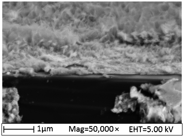
Interface edge showing submicrometre thickness
General observations
The electroless plating solutions have not yet been optimised for the process in terms of stability against spontaneous decomposition. During this work, spontaneous decomposition was controlled by slow addition of the reducing agent during the course of the reaction, which resulted in low P content in the deposits.
Elaboration of the chemical analyses of the interface can lead to much better results, in terms of both accuracy and properties. Higher accuracy can be achieved by knowing the concentration of either P or B in the alloy, which can be determined gravimetrically. Once such information is obtained, a more accurate density value of the interface can be used to determine its thickness. The AAS measurements can also incorporate a surface area factor derived from the comparison of the thicknesses recorded in SEM and chemically to compensate the irregular surfaces.
Conclusion
Diamond particles have been coated with Ni alloys containing either P or B using electroless plating techniques. Such process produced an interface having the desired properties, i.e. uniform coverage and nanometric thickness, using very simple apparatus, easily available chemicals and short processing times. Such qualities are very advantageous when compared with the technology and expertise needed for chemical vapour deposition and physical vapour deposition methods.
Footnotes
Acknowledgements
This study was carried out thanks to a grant provided by the Malta Council for Science and Technology, Project DIACOM (R&l 2010-025), IMA Engineering Services Ltd and the European Regional Development Fund (project no. ERDF 012).