
Abstract
Since its discovery, graphene has been the star material either in scientific studies or potentially technical applications. There are various methods for preparation of graphene films (e.g. mechanical exfoliation, epitaxial growth, molecular assembly, chemical vapour deposition, thermal photocatalysis, and chemical or electrochemical reduction of graphene oxide). In this article, we briefly reviewed the growths of three-dimensional graphene films on metallic and non-metallic substrates using plasma enhanced chemical vapour deposition by emphasising on their growth mechanisms. Since this technique is still in its early stage, the general absence in understanding of the graphene growth processes is thus needed to be clarified. Moreover the utility of plasma enhanced chemical vapour deposition allows synthesis of graphene films at relatively low temperatures and therefore it is possible to directly grow graphene on the substrates that could not survive at high temperatures.
Introduction
Graphene is a single layer of carbon (C) atoms arrayed in a two-dimensional (2D) hexagonal structure with C–C distance of 0·142 nm. Since formally discovered in 2004, 1 it bas been the most studied material, not only because of the academic purposes but also its potential applications in various fields due to its unique optical, electronic, mechanical, and thermal properties2–10 as indicated in Fig. 1. Besides the common methods applied for graphene syntheses such as, chemical or micromechanical exfoliation of graphite, epitaxial growth from silicon carbide (SiC) substrate, chemical vapour deposition (CVD), and thermal, photocatalytic, chemical, or electrochemical reduction of graphene oxide and fluorographene, graphene has also been prepared using ion implantation method, and intercalation, ultrasonic heating, acid treatment, and arc discharge techniques. 11 Mechanical exfoliation could produce the highest quality and highest mobility graphene flakes from highly oriented pyrolytic graphite. However, it is a time consuming process and limited to a small scale production. Thermal decomposition of SiC in ultra-high vacuum chamber at high temperatures is capable of generating wafer-scale graphene layers. Unfortunately, using this technique it is difficult to control the number of graphene layers, and the interface effect with the SiC substrate could not be ignored. 12 By consideration of both film quality and price, CVD is the optimised way to produce graphene films. Conventional CVD process is usually performed in a high temperature furnace at low pressure. A primary issue with traditional CVD is the thermal expansion that results in ripples between synthesized films and the substrate, which may be alleviated at a low temperature synthesis process such as plasma enhanced CVD (PECVD). In addition, growth of graphene at low temperatures would widen the range of potential substrates that could not survive at high processing temperatures. 13
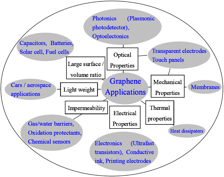
Potential applications of graphene in different fields of science and technology
Plasma is the fourth fundamental state of matter, in which a significant portion of the atoms or molecules are ionised. A typical plasma ball is presented in Fig. 2, 12 which, to some extent, behaves like a gas. PECVD is a process recently used to deposit thin films from gaseous precursors on solid substrates. It often yields fast deposition rates and maintains high film quality if compared with thermal/electron beam evaporation or sputter deposition, Because the non-equilibrium nature of the plasma contributes to the very high dissociation rates of molecular gases and thus the creation of a large number of reactive atomic and radical species. Plasma offers the possibility in production of large scale graphene films.15–17
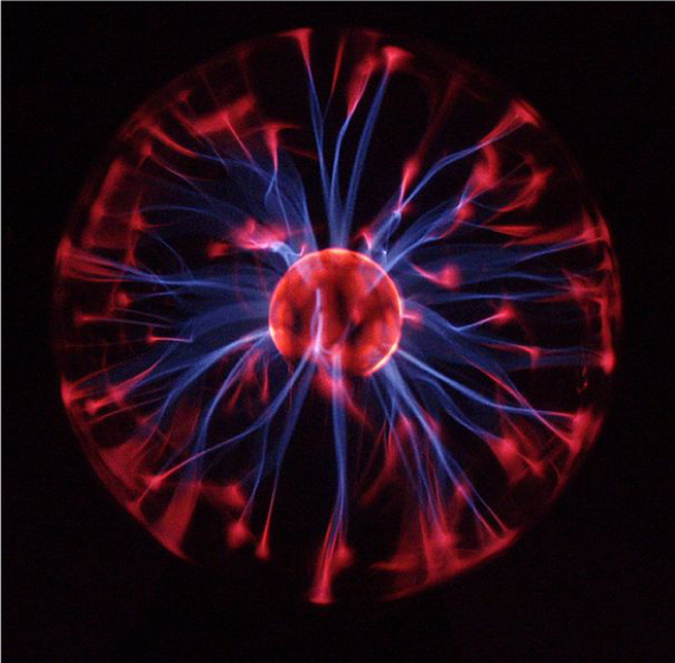
Typical plasma ball 14
In this article, we focus on the utility of PECVD in synthesis of three dimensional (3D) graphene films. It was found that the growth mechanisms are quite different on different substrates and with or without catalysts. Therefore, the initial stages of 3D graphene grown on metallic and non-metallic substrates are discussed separately.
Growth of 3D graphene films
On metallic substrates
The vertical growth of graphene films on metallic surfaces using PECVD is a rather complicated process.18,19 Choice of carbon species, property of the substrate surface, the reaction pressure and temperature, and as well as the cooling process are considered to play a crucial role in the formation of the resultant films.20–24 Simply considering the factor of surface energy, the formation of vertical wall-like structure suggests the occurrence of anisotropic process, 25 which is induced by the directed flux of carbon radical in plasma atmosphere. Zhu et al. 21 have reported that first a few nm thick parallel carbon layers are formed on the substrate surface. The vertical growth starts after a sufficient force accumulated at the grain boundaries, which push the graphene flakes to curl upward along the plasma sheath. Then the high surface mobility of the incoming carbon bearing species and the induced polarisation associated with the local electric field help the carbon nanostructure to grow vertically rather than parallelly. The ionised hydrogen in the plasma offers an etching function, which rapidly removes the amorphous carbon defects to prevent the formation of secondary nuclei that might interfere with the growth, and also to remove the cross-linking at the free edges of the vertically growing carbon sheets to keep the edge thinning. 26 The underlying mechanism is related to the reduction in the surface energy per unit area upon surface hydrogenation. This in turn makes it possible to increase the surface area by bending the graphene sheet without increasing the total surface energy. Hydrogen plasma can also be used for highly selective low temperature etching of graphene edges without introducing defects in the basal plane. 27
Recently, 3D graphene was obtained on the Ni foil substrate using microwave PECVD in CH4/H2 plasma as shown in Fig. 3a. 28 The 3D graphene growth process using PECVD should be different from that using conventional CVD process, where carbon diffuses into the Ni bulk phase at high temperature and then emerges out to the surface to form graphene as the temperature is reduced. 29 Highly energetic reactive species, e.g., CHx and excited H atoms and ions are generated in the plasma, which may lead to direct growth of graphene on the substrate surface as reported previously on the stainless steel substrate. 30 The transition electron microscopy (TEM) and high resolution TEM (HRTEM) images (Fig. 3b and c) show that the graphene films consist of multilayers as highlighted in the white box. Meanwhile, the corresponding intensity of the graphene is shown in Fig. 3d. The thickness of each graphene layer is measured to be 0·34 nm, which is consistent with the theoretical thickness of monolayer graphene. Figure 4 shows the typical Raman spectrum collected on the as grown 3D graphene on Ni substrate. 31 Besides a G band at 1586 cm−1, a D band at 1340 cm−1, and a 2D band at 2668 cm−1 are found, which is associated with the sp2 in plane phonon vibrations, assigned to defect mediated phonons near the Brillouin zone (BZ) edge (near the K-point), and originated from a second-order degenerate (iTO and LO) phonon process, respectively. A faint D’ feature at 1621 cm−1 accompanied with a D+D’ overtone at 2940 cm−1, originating from an intravalley process is also observed. The appearance of the D band with an intensity comparable to that of the G band implies that the synthesised graphene films were defective. The crack formation in graphene layers grown by a plasma assisted process was suggested to serve as sites for the growth of stand-up graphene sheets.
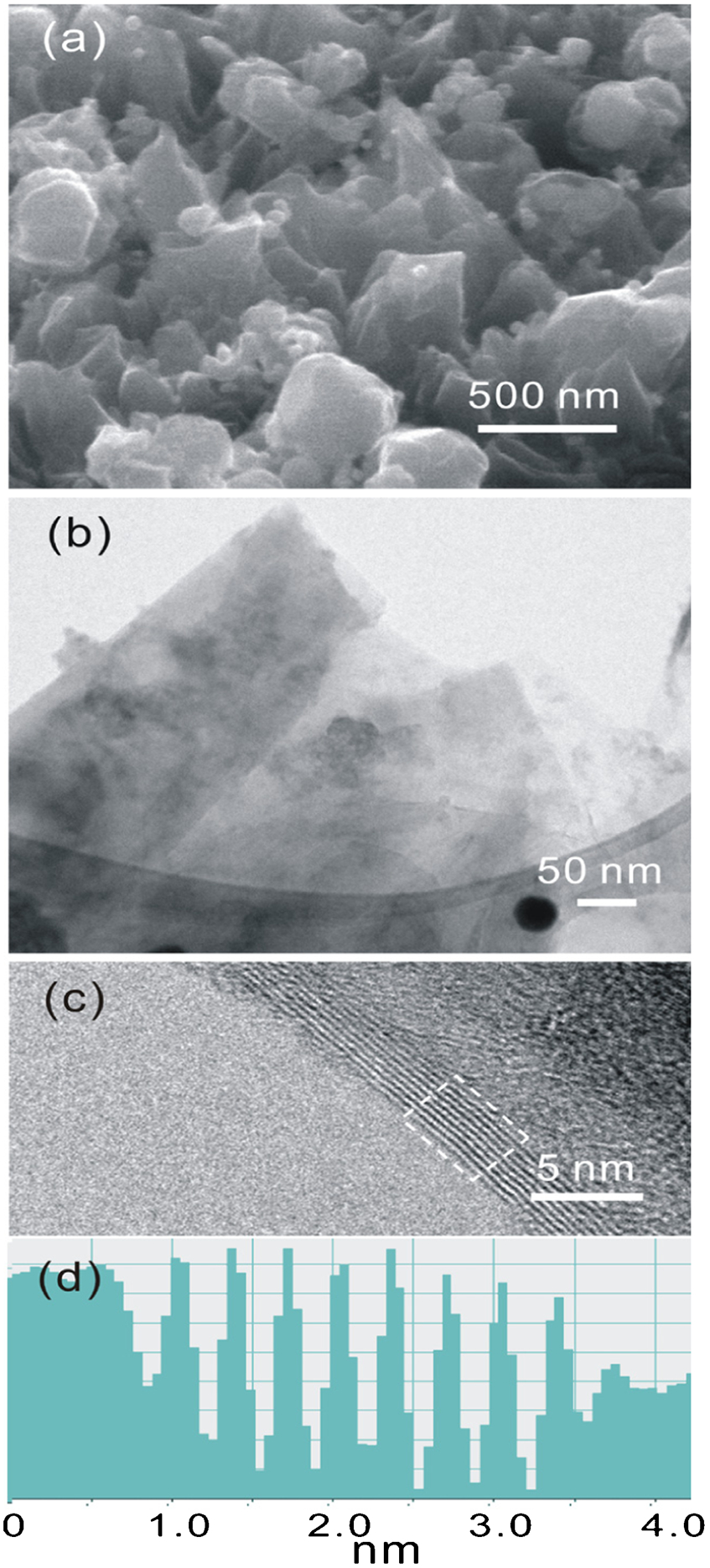
a scanning electron microscopy (SEM) image of as prepared 3D graphene films on Ni substrate measured at 45°, b transition electron microscopy (TEM) and c high resolution TEM (HRTEM) images of as synthesised graphene, d corresponding intensity profile of multilayer graphene shown in c as emphasised in white box, by which thickness of monolayer graphene sheet can be determined: adapted from Ref. 25 with permission from Royal Society of Chemistry
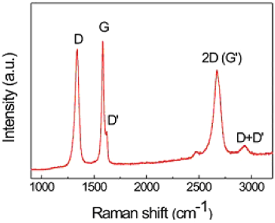
Raman spectrum of as grown 3D graphene architectures on Ni foil. Reproduced from Ref. 28 with permission from Royal Society of Chemistry
Bo et al. 32 have designed a continuous synthesis device for growth of vertically oriented graphene sheets on cylindrical wire substrates using an atmospheric PECVD system, which combines a U-shaped reactor design with ‘dynamic mode’ synthesis featuring simultaneous rotational and axial movements of the metallic wire substrate. The new setup can enable continuous synthesis of vertical graphene sheets on the wire surface with remarkable uniformity in both circumferential and axial directions. 32 The vertically oriented graphene films grown using radio frequency PECVD on Ni substrate were used as electrode in electric double layer capacitors. 33 The specific capacitance of the device fabricated with these films was enhanced following a linear relationship with growth time and finally achieved a value greater than 120 μF cm−2 at 1 kHz. An impedance phase angle of −45° was reached at 30 kHz. The normalisation of specific capacitance to growth height implies that it is not double layer charge storage on planar surface area.34–36
SEM results of various synthesis times revealed a three-step growth mechanism for few-layer graphene (FLG) on the Pt substrate as presented in Fig. 5. 30 In the initial step, a base graphite layer is formed parallel on the Pt surface, which is not continuous but shows many irregular cracks. Internal stress due to mismatch between the lattice parameters of Pt and graphite are thought to be the main reason for the formation of cracks. Freestanding FLG nucleates from these upward curling crack edges in the second step, fundamentally varying their growth direction from parallel to vertical against the substrate surface. After the initiation of the vertical growth process, the third step comprises the accumulation and incorporation of carbon radicals at the edges of the freestanding FLG. Similar results are also reported on the Ni substrate, the graphene grown on the Ni grain boundaries of substrate shows a faster growth rate, but more disordered structure than in the centre of the Ni grains. 33 At a few nm away from the grain boundaries the graphene grew vertically at a rate of 70–80 nm per minute. Raman spectra indicated that the intensity ratio of the D to G band gradually decreased with the growth time toward a value of about 0·5. This suggests that the crystalline order of the vertical graphene increases with height.
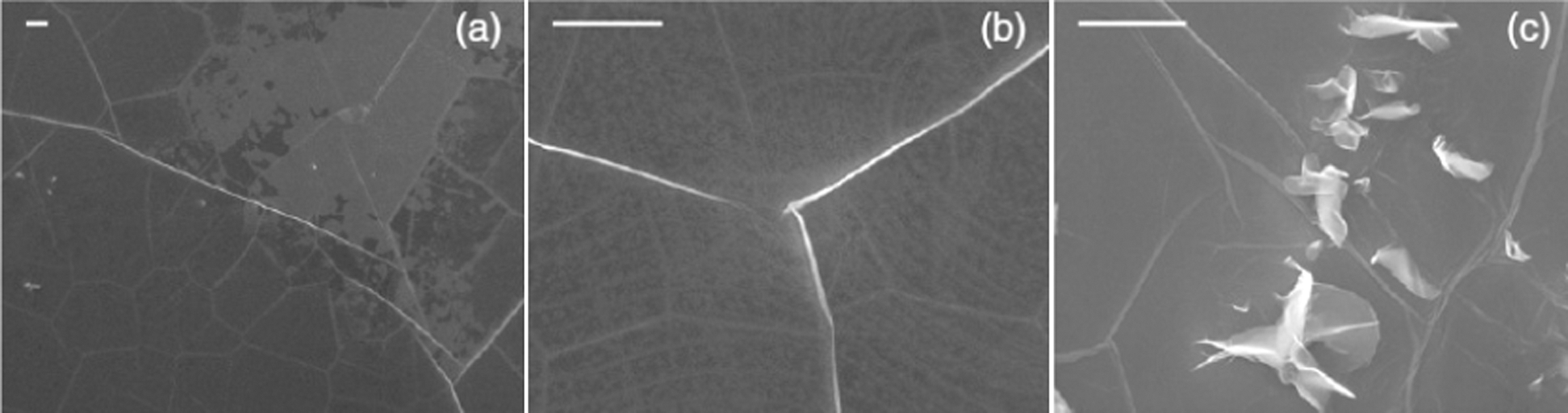
SEM images of three-step growth mechanism of FLG on Pt substrate: a in first step, graphite base layer is formed parallel to substrate surface, which shows many irregular cracks over its entire surface area; b in second step, upward curling crack edges are nucleation sites for vertical few layer graphene; c third step comprises accumulation and incorporation of carbon radicals at edges and sides of freestanding FLG; scale bars correspond to 1 μm; reproduced from Ref. 27 with permission from IOP publishing Ltd
On non-metallic substrates
Four to six multilayer graphene aligned vertically to the Si and SiO2 substrate surfaces was synthesised in the absence of any metallic catalyst by microwave PECVD in CH4 and H2 atmosphere.37,38 Interestingly, the direct growth of graphene on the Si surfaces has only been possible when the surface is exposed to the plasma. Despite a large number of proposed models, there is currently still no clear understanding of these striking experimental observations. 39 The constitutive graphene films possess a highly graphitised knife edged structure with a 2–3 nm thick sharp edge as revealed by TEM. 40 Figure 6 shows the SEM and atomic force microscopy (AFM) images of the vertically grown graphene nanoflackes. It can be seen that the flower-like nanosheets have crumpled surfaces and arbitrarily intertwine each other with a large surface area. The special nest-like morphology and large surface area of vertical graphene films present a distinct opportunity for creating a new class of electrodes for a wide range of applications in the electroanalytical, biosensing, energy storage/conversion sectors.40–42 It shows excellent kinetics in electron transfer for the Fe(CN)6 3−/4− reduction/oxidation system 39 and superior electrocatalytical activity for simultaneous determination of dopamine (DA), ascorbic acid (AA), and uric acid (UA). 38 This unique edge-plane-based electrochemical platform with high surface area and electrocatalytical activity provides great opportunity for creating a revolutionary new sort of nanostructured electrodes used in biosensing, biofuel cells and energy conversion.
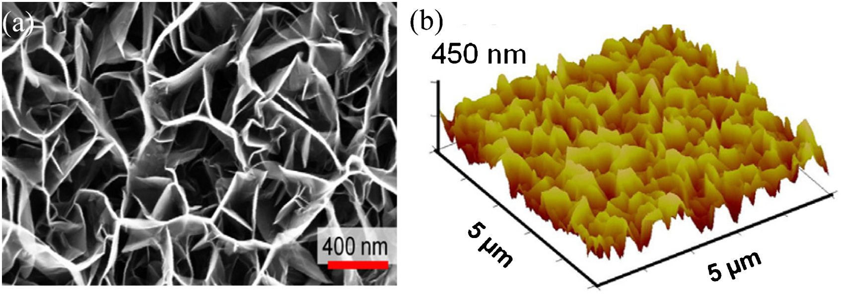
a high magnification SEM and b AFM image of vertical graphene nanoflackes: reproduced from Ref. 33 with permission from Elsevier
Soin et al. 39 pointed out that the graphene growth can orientate in two directions: parallel and vertical to the substrate. The parallel growth will stop when the graphene edge gets contact with another one. When every line segment is blocked, parallel growth will completely cease and vertical growth dominates the process. It was proposed that the in-plane nucleation sites evolve via the addition of C2 radical to the 2D graphene clusters that are formed during the initial nucleation phase as shown in Fig. 7a. Once the sheet geometry is changed from in-plane to out-plane via stress release, the high mobility of the incoming carbon bearing species induces polarization of graphitic layers and consequently causes graphene to grow perpendicularly as shown in Fig. 7b. Zhang et al. 43 found that when the direct current (DC) voltage is decreased to 50 V, no vertically grown graphene is formed. It is thus believed to us that the strong electric field force is another main factor that causes the graphene to polarise vertically to the substrates.21,44,45 It is plasma who makes it possible to enhance the surface area by bending the graphene sheet without increasing the total surface area.27,46–48 When smaller petals merge and thus form a larger interconnected network, the resultant petal structure becomes an electrostatic equipotential surface, reducing the effect of the inhomogeneous and local electric field distribution, then leading to a more uniform growth of graphene sheets. Figure 8 shows the different shapes and densities of vertical graphene sheets at different growth time.
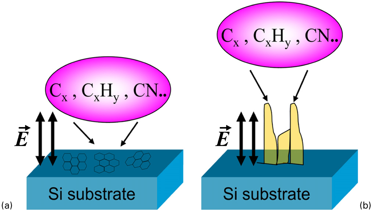
Schematic illustration of growth model of FLG: a initial nucleation stage of in-plane turbostratic graphite via carbon radical precipitation or adsorption onto silicon substrate and b subsequent change in orientation with increase in growth time leading to formation of vertical FLG; reproduced from Ref. 33 with permission from Elsevier
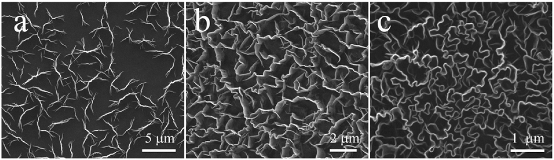
a–c SEM images of FLG sheets, showing their different shapes and densities for different growth times: from Ref. 35: a 5 min; b 20 min; c 60 min
A model for the initial growth mechanism of graphene has been proposed using CFx as the carbon precursor on the Si substrate. 49 Initially, CFx radicals are adsorbed on the Si surface to form a very thin fluorocarbon layer. Then carbon species produced from the CFx radicals adsorb on or migrate on the Si surface via the F abstraction reaction by H radicals and condense to form carbon nanoislands with active dangling bonds. When the deposition time increases, the Si substrate surface is completely covered by the carbon nanoislands and an interface layer with a rough surface is formed, on which there are many dangling bonds acting as nucleation sites for carbon nanoflakes. Consequently, small and disordered carbon nanoflakes are nucleated at these dangling bonds following a 2D growth model and subsequently form nanographene sheets. Finally among the randomly orientated graphene sheets, those standing vertically on the substrate surface grow faster than those parallelly lay down on the substrate resulting in the formation of vertical graphene nanosheets. This is because that the growth rates are different along the strongly bonded planes and along the weakly bonded stacking direction of the expanding graphene sheets. Reactive carbon radicals arrive easily and firstly at the edge of the graphene layer, and at the same time the graphene layers expand preferentially in the radical diffusion direction that is perpendicular to the electrode plane.
The electric field emission behaviour of vertically aligned 4–6 layer graphene on Si was studied. 37 The FLG was found to be a good field emitter characterized by turn-on fields as low as 1 V m−1 and field amplification factors up to several thousands. FLG grown with a large H2/CH4 gas ratio revealed improved field emission when compared to with a small H2/CH4 gas ratio. This can be linked to the fact that a higher H2 gas ratio results in etching of unwanted amorphous carbon, thereby also sharpening FLG edges. Finite element modelling indicates that, due to electric field screening, only a small percentage of FLG nanostructures being at least 10% higher than the average height and positioned at a distance of several micrometers from each other contribute to field emission. 37 The field emission characteristics were found to be strongly influenced by the tip shape, the height, and the amorphous carbon content.43,50 The optimal shape of vertical FLG for field emission had fewer layers, sharp corners, large height and free of amorphous carbon. Qi et al. 51 adopted argon plasma treatment to improve the shape of FLG as a high performance field emitter.
Conclusion
Growth of 3D graphene films on metallic and non-metallic substrates using PECVD has been summarised. The non-equilibrium property of the plasma induces very high decomposition rates of the molecular gases. It not only accelerates the growth rate of graphene, but also provides energy for vertical growth of graphene layers. The graphene growth mechanisms on different substrates are different. The initial stages of vertical graphene were various for different substrates due to their distinct physics natures.
On the metallic (Pt) surface, the formation of surface cracks caused by the lattice mismatch is the nucleation sites for vertical growth. However, on the non-metallic surface, the vertical growth starts when two flatly grown graphene sheets get contact each other. Owning to the unique structure and excellent properties of 3D graphene in electronic, they have been widely applied in FET devices and showed better properties than those of 2D graphene films.
Footnotes
Acknowledgements
Wu would like to thank Quanzhou ‘Tong-Jiang Scholar’ program, Fujian ‘Min-Jiang Scholar’ program, program for New Century Excellent Talents in University (NCET-13-0879), the Education and Scientific Research Foundation (Class A) for Young Teachers of Education Bureau of Fujian Province, China (grant no. JA13263), and National Natural Science Foundation of China (grant no. 21353001) for financial supports.