
Abstract
Hydrogenated silicon thin films were deposited using plasma enhanced chemical vapour deposition method. The effects of substrate temperature on the microstructure and electrical properties of the films were investigated. Results show that the as received crystalline silicon thin film is a typical two-phase structure consisting of an amorphous phase and a crystalline phase. At a lower substrate temperature, the thickness of the initial amorphous incubation layer is dozens of nanometers, and few crystalline grains inset in the film after phase transition. As the substrate temperature increases, the initial incubation stage shortens to several nanometers, and the phase transition to crystalline starts earlier. After the phase transition, abundant crystallites appear, and the amorphous phase exists in the film just as the grain boundary. However, at overhigh substrate temperature, the average crystallinity and grain size of the film decrease. Deposition rate abidingly decreases with the increase in substrate temperature. The films with more ordered structure exhibit superior electrical properties.
Introduction
Silicon thin films have been studied extensively as promising materials for applications in solar cells due to their natural abundance, environmental safety, potential high performance and capability of low cost production.1–4 Plasma enhanced chemical vapour deposition (PECVD) is used widely for the preparation of silicon thin films on a large area substrate and at low substrate temperature.5–7 However, it has been recognised that amorphous silicon thin films suffer light induced degradation, resulting in a reduction in the power conversion efficiency of the device.8,9 The light induced degradation is attributed to an intrinsic phenomenon typical of the disorder network consisting of Si and H, which forms metastable Si dangling bond defects and acts as recombination centres for electron–hole pairs and consequently decreases the photocarrier lifetime.
To overcome the degradation of amorphous silicon thin films, hydrogenated crystalline silicon thin films have been prepared from SiH4 gas heavily diluted with H2. The mechanism of hydrogen induced crystallisation of silicon thin films has been proposed by three models, namely surface diffusion model, 10 etching model 11 and chemical annealing model. 12 Hydrogenated nanocrystalline or microcrystalline silicon thin film is a kind of two-phase mixed material consisting of crystallites, amorphous phases and voids, dangling bands, etc. 13 The structure of the hydrogenated crystalline silicon thin films from substrate to surface is not uniform. It is amorphous at the early stage of deposition and then could transfer to crystalline phase with the increase in deposition time. It has been found that the structure near the interface can be significantly improved for the films deposited under high hydrogen dilution and pressure. 14 Several researchers also investigated the effect of substrate temperature on the morphological characteristics of silicon thin films prepared by PECVD.15–17 However, little attention has been paid to the investigation on the growth process in the longitudinal structure of silicon thin films, particularly the visual observation for the region near the interface and phase transition.
In the present work, intrinsic hydrogenated silicon thin films were deposited at different substrate temperatures by PECVD. In addition, their morphological evolution and phase transition from amorphous to crystalline during the early nucleation and the later growth stages were investigated. This work will provide scientific basis for preparing hydrogenated crystalline silicon thin films with uniform microstructure and high performance.
Experimental
Hydrogenated silicon thin films were deposited onto n type monocrystalline silicon in a single chamber PECVD system at radio frequency (RF, 13·56 MHz) power with substrate temperatures of 100, 150, 200 and 250°C, respectively. The mixture with gas flow ratios of SiH4/H2 = 7:200 (in standard cubic centimeter per minute) was used as gas source. The RF power of 100 W, deposition time of 120 min and pressure of 40 Pa were maintained constant for all of the samples.
The microstructure of the films was characterised by a combination of X-ray diffraction (XRD) and high resolution transmission electron microscopy (HRTEM) observations. The XRD-7000 XRD was carried out using a conventional Cu Kα X-ray radiation (λ = 1·5418 Å) source. The HRTEM and Selected Area Electron Diffraction (SAED) observations were performed using a JEM-3010 operation. Analyses of the images and the corresponding diffraction patterns provided information about the size and orientation of the crystallites. The thickness of the films was measured from cross-sectional TEM images, and the average deposition rate was derived from the corresponding thickness. The dark conductivity was measured with a co-planer Au electrode deposited at room temperature, and the minority carrier lifetime was studied using a Semilab-WT1000 minority carrier lifetime tester.
Results and discussion
High resolution transmission electron microscopy characterisation
The crystalline silicon thin film is a typical two-phase structure consisting of an amorphous phase and a crystalline phase. There could be a hatching layer near the substrate surface for the phase transition from amorphous to crystalline. 18 The structure of the films is amorphous at the early stage of deposition and then could transfer to crystalline phase with the increase in deposition time. As the thickness increases, both grain size and crystallinity increase.
Figures 1–4 display the changes in longitudinal microstructure of the films upon increasing the thickness for each substrate temperature. The figures marked in (a) are the SAED patterns for the integral films, and the figures marked in (b), (c) and (d) stand for the regions of interface, after phase transition and nearing film surface respectively to study the structural evolvement from substrate to film surface.
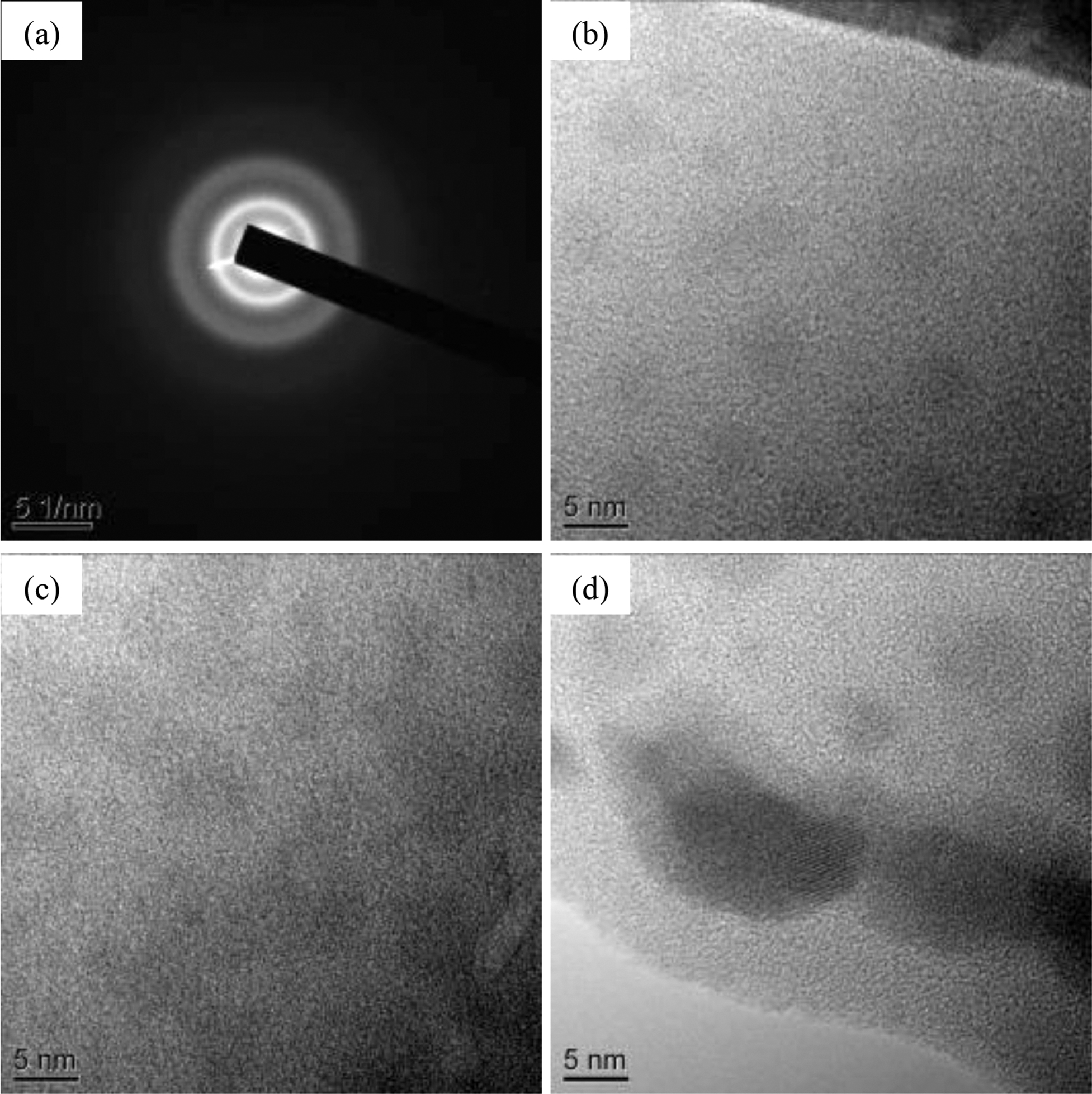
SAED pattern and HRTEM images of silicon thin film obtained at substrate temperature of 100°C
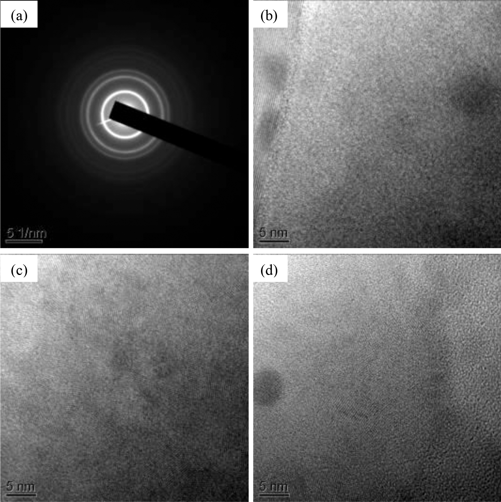
SAED pattern and HRTEM images of silicon thin film obtained at substrate temperature of 150°C
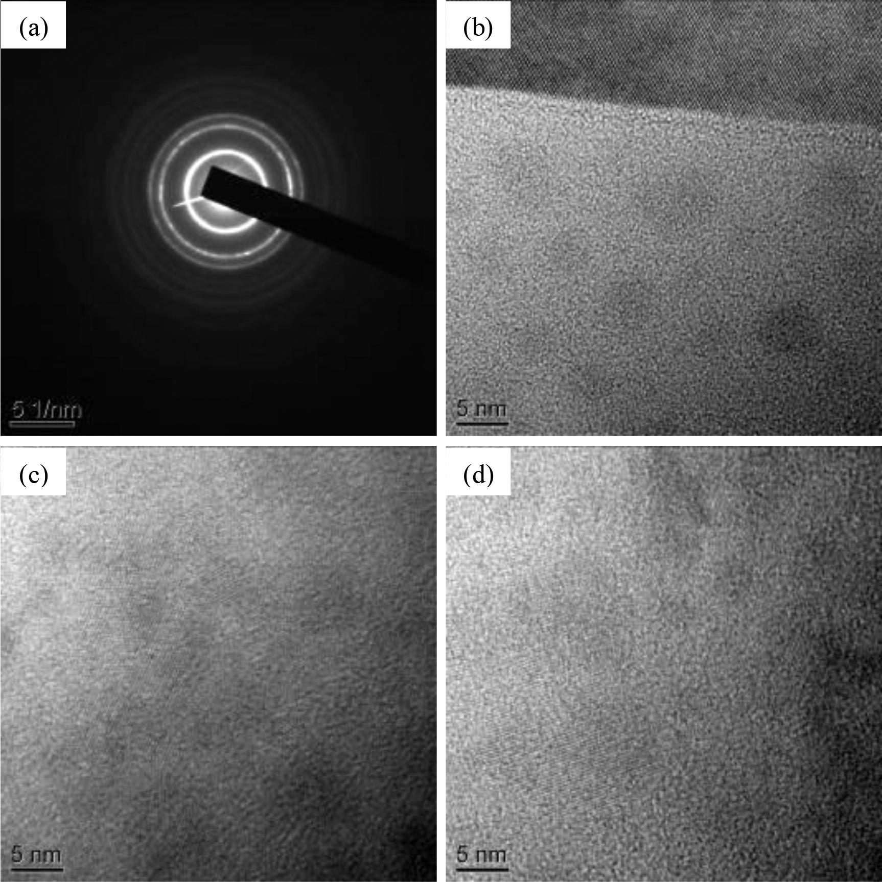
SAED pattern and HRTEM images of silicon thin film obtained at substrate temperature of 200°C
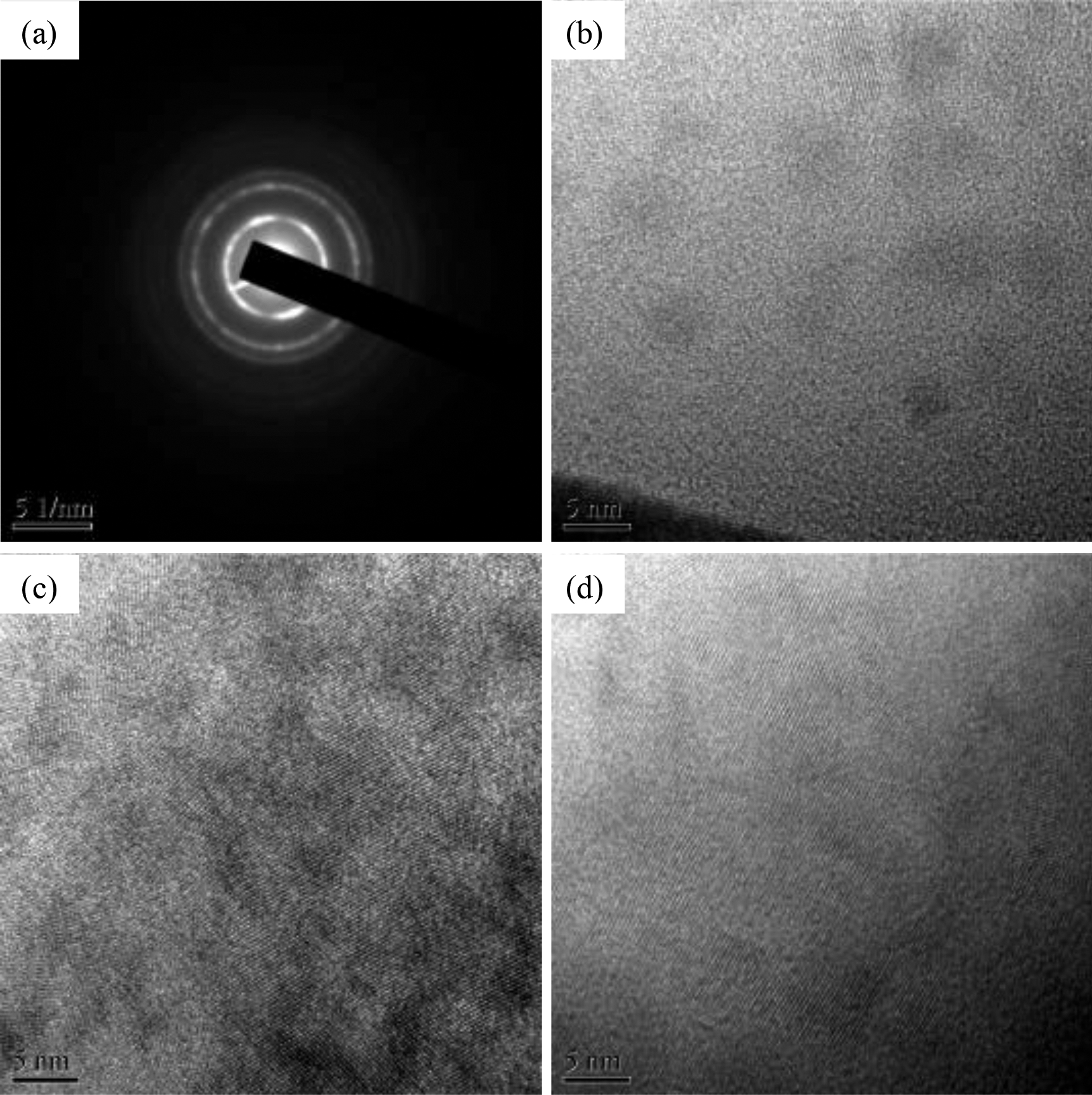
SAED pattern and HRTEM images of silicon thin film obtained at substrate temperature of 250°C
From the figures, it is observed that the deposition process of the film can be divided into three stages of structure change, that is, the initial nucleus incubation stage with predominantly amorphous phase, the phase transition stage where crystallites appear and grow, and the crystalline deposition mode stage with highly crystalline phase.
When the substrate temperature is 100°C, the amorphous layer is 30 nm in thickness (Fig. 1b). With the increase in thickness, isolated crystalline grains with around 2 nm inset in the film (Fig. 1c). Nearing the film surface, there is still largely an amorphous phase with a finite amount of crystallites in the film (Fig. 1d), although the grain size increases to around 5 nm.
Improving the substrate temperature, the thickness of the amorphous layer decreases to about 25 nm for 150°C (Fig. 2b), 10 nm for 200°C (Fig. 3b) and 5 nm for 250°C (Fig. 4b), which illustrates that the initial nucleus incubation stage shortens and the phase transition to crystalline starts earlier. After the phase transition, it is found that the amount of crystalline grains appears and the amorphous phase exists in the film just as the grain boundary. The grain size increased to 5 nm for 150°C, 10–20 nm for 200°C and 10–15 nm for 250°C. Moreover, the crystalline volume fraction is more than 90%, and the grain size increased to several tens of nanometers near the film surface. In particular, the grain size comes up to 40 nm when the substrate temperature is 200°C (Fig. 3d).
From the SAED patterns, it could be observed that the discrete spots superimposing on the continuous rings seemed brighter as the substrate temperature was increased, which is the typical characteristic of the microcrystalline structure. According to the standardisation of diffraction rings, it is found that they correspond to Si (111), Si (220) and Si (311) crystal planes respectively, which confirms also the XRD studies.
The dominant growth mechanism of the deposition precursors in the hydrogenated silicon thin film is passed through direct adsorption on the surface dangling bonds. 19 With an increase in substrate temperature, each deposited atom receives sufficient energy, and its surface mobility increases. This improves their diffusion lengths and allows them to reach favorable low energy sites, namely crystal plane. In addition, the density of defect state in the films decreases. As a result, the formation of crystallites is easier and earlier as well as the grain size is bigger.
To gain uniform longitudinal structure from the substrate surface to the film surface, substrate temperature should present a graded distribution in the deposition process just as hydrogen dilution. In the initial deposition stage, high substrate temperature and hydrogen dilution are necessary. Then, with increasing deposition time, both substrate temperature and hydrogen dilution should decrease gradually.
X-ray diffraction study
Figure 5 shows the XRD patterns of the films obtained at different substrate temperatures. It can be seen that no crystalline Si peaks appear on the film obtained at 100°C, and the film expresses amorphous as a whole. For the film deposited in the other three conditions, three prominent individual peaks corresponding to the Si (111), Si (220) and Si (311) crystal planes have been identified in the diffraction spectra at 2θ angles of 28·442, 47·302 and 56·121° respectively. It is noted that the film has preferential orientation along the Si (111) peak since this orientation has the lowest free energy. 20 With the increase of substrate temperature, it can be seen that the intensity of Si (111) peak increases firstly and then decreases, while the full wave at half maximum becomes narrowed firstly and then widens. It indicates that the crystallinity and average grain size increase firstly and then decrease with increasing substrate temperature. The results verify the HRTEM results.
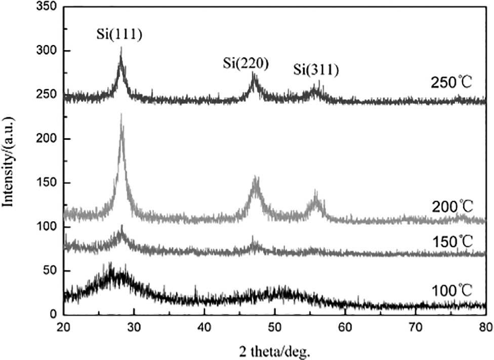
X-ray diffraction patterns of films obtained at different substrate temperatures
Improving the substrate temperature can result in the increase of diffusion length of the deposited atoms, which is beneficial to the diffusion of deposited atoms to the position with the lowest energy and the formation of crystalline grains. Simultaneously, the hydrogen content in silicon based film, which is a key factor leading to the crystallisation of silicon film, has a direct relationship with the substrate temperature. It is that the hydrogen content in the film decreases with increasing substrate temperature under certain conditions. 21 Therefore, when the increase in diffusion length of the deposited atoms is better than the decrease in hydrogen content in the film, improving the substrate temperature strengthens the crystallisation of the films. However, at overhigh substrate temperature, there is not enough hydrogen to compensate the dangling bands on the film surface, although the diffusion length of the deposited atoms increases, which weakens the crystallisation of the films. The opposite effects of substrate temperature on the diffusion length of deposited atoms and hydrogen content suggest that an optimal temperature is possible for the deposition of the film.
Variation in deposition rate
The variation of deposition rate as a function of substrate temperature for the films is shown in Fig. 6. As seen from the figure, the deposition rate of the films decreases from 5·52 to 1·76 nm min− 1 as the substrate temperature increases from 100 to 250°C.
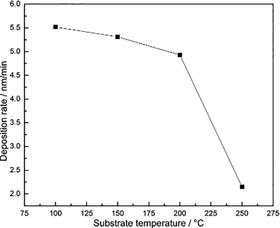
Variation of deposition rate as function of substrate temperature for films
This change trend is different from the XRD results. It can be attributed to the increase of silane desorption from the film surface. 22 As the substrate temperature increases, the diffusion length of the deposited atoms on the film surface increases. These atoms have high activity so that they are easily bombarded by subsequent deposited atoms and desorption from the film surface is improved. Consequently, the deposition rate has a continuous decrease with increasing substrate temperature. The decrease in deposition rate as the substrate temperature increases was reported 23 previously for microcrystalline silicon thin films. In turn, the decreasing deposition rate demonstrates that the deposited atoms have enough time to remove to the equilibrium position at higher substrate temperature, which agrees with the HRTEM results.
Electrical properties
The variation of dark conductivity and minority carrier lifetime as a function of substrate temperature for the films is shown in Fig. 7. It is seen from the curves of dark conductivity and minority carrier lifetime that their values are maximum for the film deposited at substrate temperature of 200°C, whereas they are smaller at lower and higher substrate temperature than 200°C. The dark conductivity differs by three orders of magnitude, and the minority carrier lifetime has a weaker change upon increasing the substrate temperature. As seen from the figure, the dark conductivity increases from 9·866E-4 S cm− 1 at 100°C to 2·19E-1 S cm− 1 at 200°C and then decreases to 6·07E-2 S cm− 1 at 250°C, and the minority carrier lifetime increases from 7·9 μs at 100°C to 16·91 μs at 200°C and then decreases to 14·23 μs at 250°C.
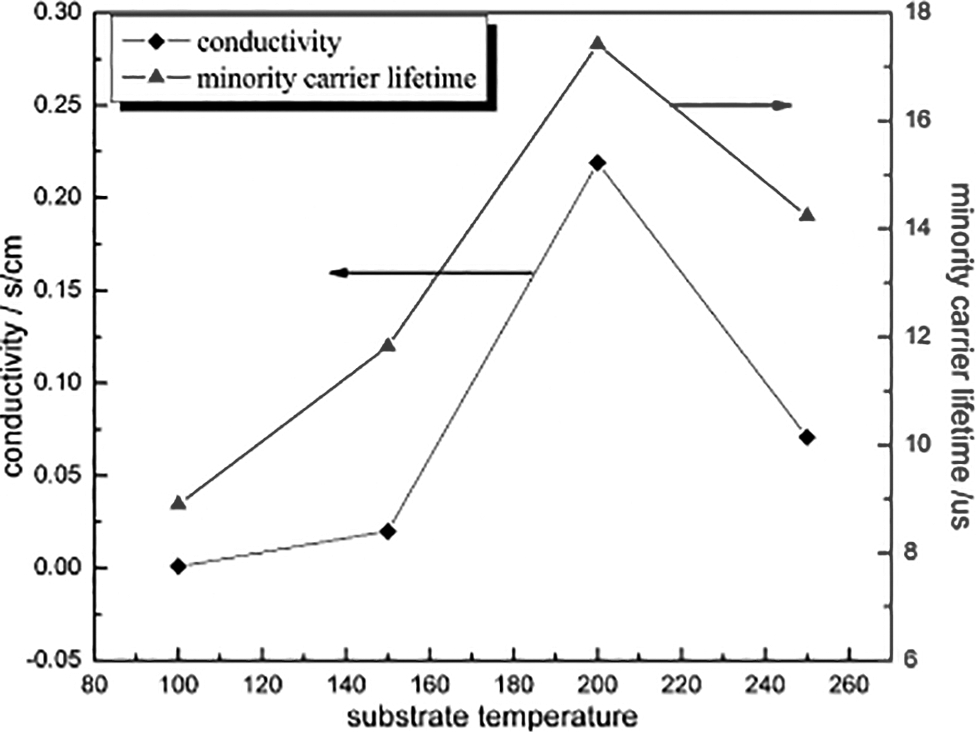
Dark conductivity and minority carrier lifetime of films at various substrate temperatures
The data of both series exhibit similar change trend with the XRD results, which shows an expected correlation between the electrical properties and the microstructure of silicon films. The defects in the film are the recombination centres for the minority carrier. 24 Therefore, the minority carrier lifetime is responsible for the density of the defect state. The film with higher order degree has lower density of defect state; consequently, the minority carrier lifetime is longer. Moreover, dark conductivity is dominated by the surface near crystalline part of the films. 25 The film obtained at the substrate temperature of 200°C has the biggest crystalline volume fraction and grain size nearing the film surface, as shown in HRTEM pictures; as a consequence, the highest dark conductivity is possible.
Conclusion
Hydrogenated silicon thin films were deposited using PECVD method at different substrate temperatures. The structure of the films with two-phase structure is amorphous in the initial deposition stage and transfers to crystalline with the increase in thickness. Both crystallinity and grain size also improve as the deposition time increases. With the increase of substrate temperature, the thickness of the amorphous layer decreases, and the phase transition to crystalline starts earlier. But at overhigh substrate temperature, the crystallinity and grain size decrease. Similarly, the electronic properties of the films increase firstly and then decrease with the increase of substrate temperature. This is attributed to the opposite effects of substrate temperature on the diffusion of deposited atoms and the content of hydrogen on the film surface. Consequently, the deposition rate continues to decrease with the increase of substrate temperature. To gain uniform longitudinal structure from substrate surface to film surface, it is necessary that substrate temperature and hydrogen dilution are high in the initial deposition stage and then decrease as the deposition time increases to form a graded distribution.
Acknowledgements
This work has been supported by the National Natural Science Foundation of China under grant no. 51221001, the ‘‘111’’ Project under grant no. B08040 and the National ‘‘973’’ Project of the People's Republic of China under grant no. 2011CB605806.