
Abstract
Phosphorus-doped ZnO (ZnO:P) films were grown on quartz substrate by radiofrequency magnetron sputtering technique using mixture gas of Ar and O2 with different mass ratios, and then the films were annealed rapidly in air ambient, the properties of ZnO:P film and p-type mechanism were investigated. A stable p type ZnO:P film was obtained by using the mixture gas with mass ratio of Ar to O2 of 1 to 0·05 at a temperature of 750°C in air ambient, which had a resistivity of 59·75∼59·86 Ωcm, a hole concentration of 2·34 × 1017∼2·11 × 1018 cm− 3 and a mobility of 0·05∼0·47 cm2 V− 1 s− 1 respectively. The shallow acceptor level was estimated to be located at 113∼125 meV above the valence band. The formation mechanism of p type ZnO:P film was related to the PZn–2VZn complex acceptors. The p-n homojunction showed typical rectification behaviour.
Introduction
ZnO has attracted significant attention in the last few years because of its suitable band gap (3·3 eV) and large exciton binding energy (60 meV) for applications in the UV region, such as photodetectors and light emitting diodes.1–3 It is well known that high quality n type ZnO film can be easily realised, but the high quality p type ZnO film is difficult to obtain due to self-compensation from native donor defects (VO) and (Zni) or hydrogen as an unintentional extrinsic donor, and also because of the low solubility of the p type dopants in the film.4,5 The realisation of p type ZnO film has an important effect on the creation of ZnO based optoelectronic devices.
Nitrogen (N), phosphorus (P), arsenic (As) and antimony (Sb)) are doped to produce p type ZnO film.6–9 Among various dopants, P seems to be one of the most promising candidates to produce p type ZnO materials due to ZnO:P thin films show good stability and reproducibility.10–13 In the p type ZnO:P film, P substitution for Zn sites (PZn) combines with two Zn vacancy complex acceptors (PZn–2VZn) and is proposed to explain the p type mechanism.14,15 The quality of the film can be influenced by the ratio of Ar and O2, which can affect the electrical and optical properties of the film and determine the related p type mechanism.
In this work, p type ZnO:P films were deposited on the quartz substrate using a ZnO/P2O5 target by radiofrequency (RF) magnetron sputtering with Ar/O2 and then under rapid thermal annealing (RTA) in air ambient. Effects of Ar/O2 ratio on the electrical and optical properties of ZnO:P films were investigated. The p type ZnO:P film can be obtained with mass ratio of Ar to O2 of 1 to 0·05, and its p type mechanism was discussed.
Experimental
ZnO:P films were grown on quartz substrate by radiofrequency (RF) sputtering using a 2 wt-% P2O5 (99·99%) mixed ZnO (99·99%) target. A distance of 5 cm was maintained between the target and the substrate. Before being loaded into the growth chamber, the quartz substrates were cleaned successively with acetone, alcohol and deionised water in an ultrasonic bath. The growth chamber exhibited a base pressure of 5 × 10− 4 Pa. High purity Ar and O2 were used as the working gas, and partial pressures of Ar and O2 were adjusted by the use of electronic mass flow meters. The total working pressure was fixed at 0·5 Pa. The target was presputtered for 10 min to clean its surface, and then, the films were deposited at 500°C for 60 min with an RF power of 100 W. Then, all the films were treated by RTA in air at 750°C for 5 min.
Film crystallinity and orientation were examined by X-ray diffraction (XRD) with Cu Kα1 radiation λ = 0·15406 nm. The films were scanned from diffraction angles 2θ of 30∼50°. The electrical properties of the films were investigated by Hall measurements at room temperature using the four-probe van der Pauw configuration. Ohmic contacts were made by soldering indium onto the films surface. Room and low temperature photoluminescence (PL) was performed to investigate the optical transitions in the film. A 325 nm He–Cd laser was used as the excitation source.
Results and discussion
The XRD patterns of ZnO:P film after RTA are shown in Fig. 1, in which no peaks associated with P2O5 appear, showing that the film is ZnO:P but not ZnO/P2O5. It can be seen from Fig. 1a and b that ZnO:P films with pure Ar or only a few O2 (Ar/O2 = 1/0·05) showed only ZnO (002) peak, indicating that the ZnO:P film had a single phase wurtzite structure and a preferred orientation along the c axis. However, with the increase of O2 content, ZnO (101) peak appeared; when the gas was pure O2, ZnO (100) peak appeared and the intensity of the peaks increased, implying that the preferred orientation of ZnO film became weak. Moreover, the full width at half maximum (FWHM) of the film with Ar/O2 = 1/0·05 was only 0·22°, indicating that the crystal quality of the film was relatively well. When the films deposited with Ar/O2 = 1/3 or pure O2 (Fig. 1c and d), ZnO (101) and ZnO (100) peaks can be found and FWHM of ZnO (002) in the films increased respectively 0·49 and 0·45°, showing that the quality of the films decreased.
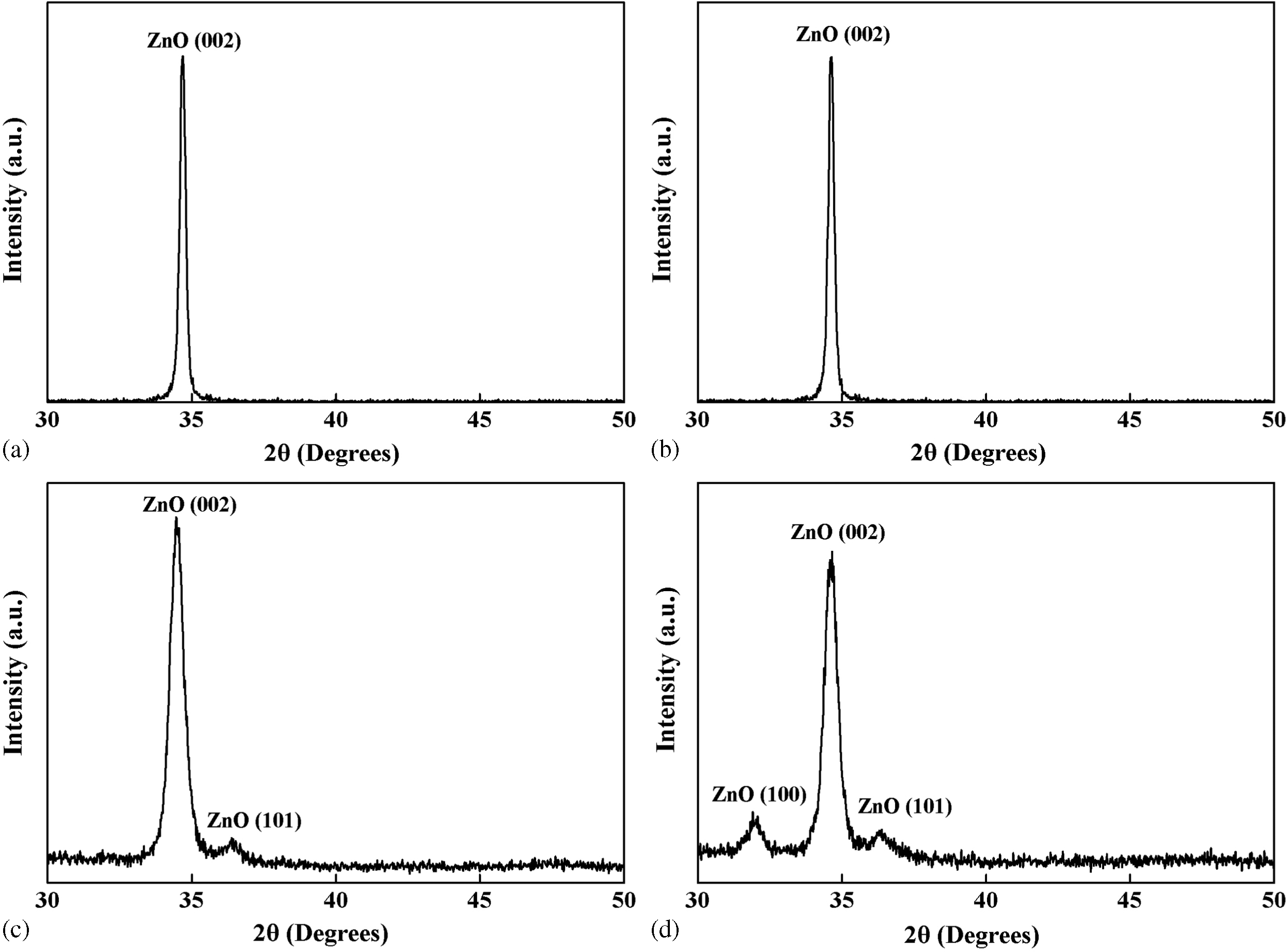
X-ray diffraction patterns of ZnO:P films with different Ar/O2 gas ratios annealed after RTA: a pure Ar; b Ar/O2 = 1/0·05; c Ar/O2 = 1/3; d pure O2
Table 1 shows the electrical properties of ZnO:P film with different Ar/O2 gas ratios. From Table 1, it was apparent that the films grown from pure Ar to pure O2 had different conductivity types, although these films were annealed under the same condition. With the increase of the O2 content, the conductivity type of the film was changing from n-p complex types to p type and then to n type. It can be found that the optimal ratio of the Ar and O2 was 1 to 0·05 to obtain p type ZnO:P film. When the film was tested again several days later, the electrical properties of p type were maintained, indicating that the p type characteristics of the film were stable. The p type ZnO:P film showed a resistivity of 59·75∼59·86 Ωcm, a mobility of 0·05∼0·47 cm2 V− 1 s− 1 and a hole concentration of 2·34 × 1017∼2·11 × 1018 cm− 3 respectively. ZnO:P films grown under a pure Ar ambient showed an n-p complex types of characteristics, even after air RTA activation, owing to the large number of native defects such as oxygen vacancies, which acted as donors and made ZnO films show n type characteristics.16,17 However, ZnO:P films grown under Ar/O2 gas ratio of 1/3 and pure O2 showed n type conductivity after the annealing process. This n type conductivity can be attributed to the formation of complex defects involving oxygen interstitials and O2 induced defects that act as donors, which can compensate the hole carriers generated by P dopant.18,19
Electrical properties of ZnO:P films with different Ar/O2 gas ratios
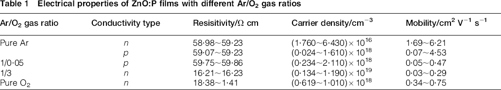
Figure 2 shows the XRD pattern of ZnO (002) peak. As shown in Fig. 2, a shift of ZnO (002) peak with a higher diffraction angle can be observed in the p type ZnO:P film with Ar/O2 gas ratio of 1 to 0·05, which meant a decrease in the lattice constant under Ar rich condition. It is known that the radius of trivalent P and bivalent Zn cation are respectively 0·44 and 0·88 nm, and the radius of trivalent P and bivalent O anion are respectively 1·86 and 1·35 nm. If P occupies an O site, the lattice constant should increase. However, if P substitutes for a Zn site, the lattice constant should decrease, consistent with the result of Fig. 2. Therefore, it is deduced that the decrease in the lattice constant of the ZnO:P is attributed to PZn.
X-ray diffraction pattern of ZnO (002) peak: a pure Ar; b Ar/O2 = 1/0·05; c Ar/O2 = 1/3; d pure O2
In order to confirm the deduction, the X-ray photoelectron spectroscopy measurement was performed for the ZnO:P films with different gas ratios. As can be seen from Fig. 3, the binding energy of P2p1/3 was found to be 133·5 eV, which was different from the binding energy of 135·5 eV observed in pure P2O5. This implied that no P2O5 clusters existed in ZnO:P films, and the P was incorporated into ZnO films during the growth process, which was in agreement with the results of XRD. The binding energies of P2p1/3 in Zn3P2 and ZnP2 are respectively 128·3 and 129·8 eV, smaller than the value in the ZnO:P, indicating that no Zn–P bond is formed in ZnO:P films. 19 That is to say, P does not substitute for O. It is well known that the PZn defect is a donor, which leads to n type conduction. 20 However, the PZn defect can combine with two Zn vacancies to form a stable shallow acceptor with a low formation energy. 21 Therefore, the p type conductivity is postulated to be associated with the PZn–2VZn complex acceptors.
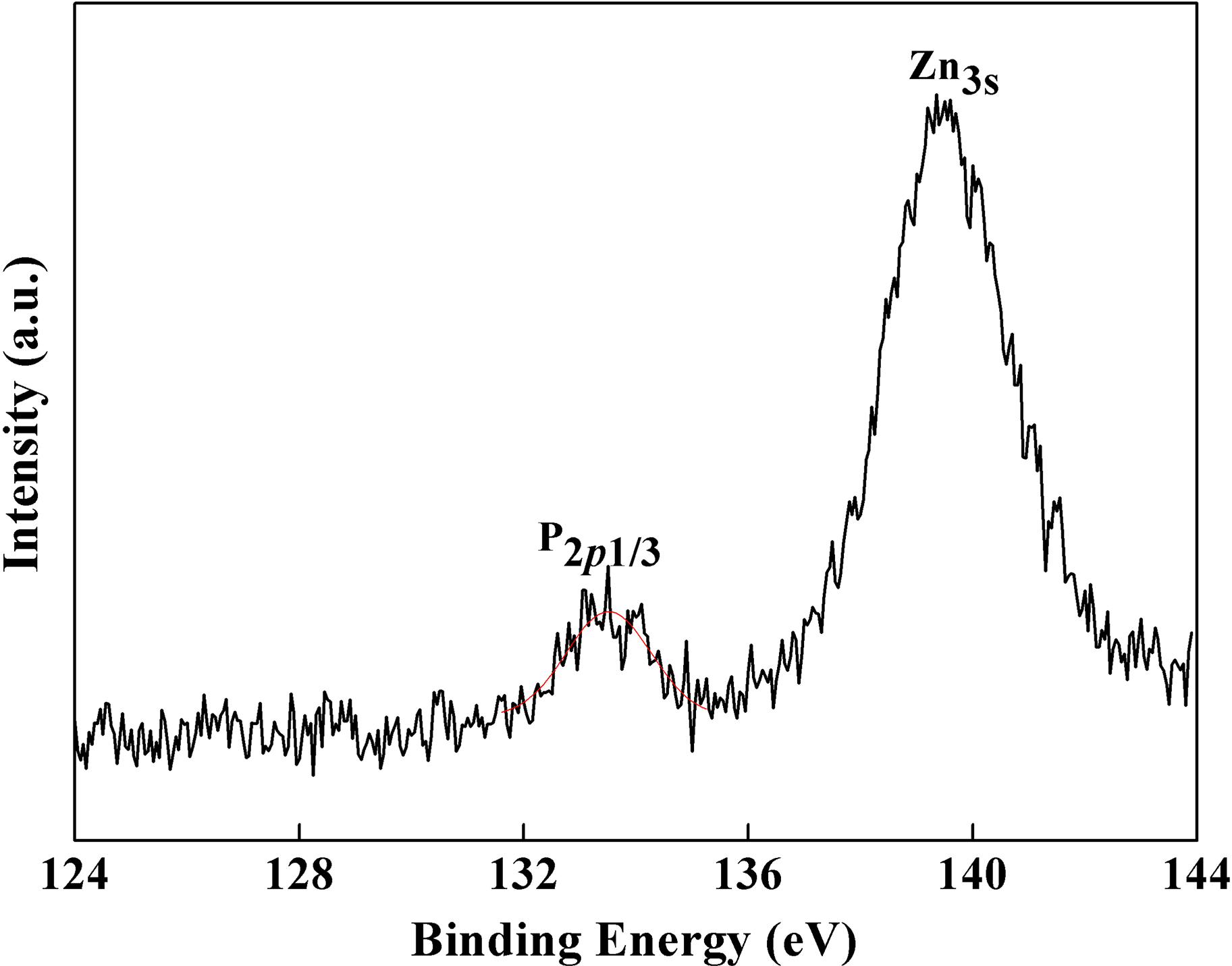
P2p1/3 X-ray photoelectron spectroscopy spectrum of ZnO:P film with Ar/O2 gas ratio of 1 to 0·05
The optical properties of ZnO:P film were conducted by PL measurements at room temperature, as shown in Fig. 4. It can be seen from Fig. 4 that all the films showed PL peaks, especially the film with Ar/O2 gas ratio of 1 to 0·05. Compared with the film with pure Ar (Fig. 4a), the film with Ar/O2 = 1/0·05 (Fig. 4b) had higher PL peak and lower FWHM, indicating that the quality and properties of the film became better. With the increase of O2 content in the films (Fig. 4c and d), the PL peak became weak and deep level defects emitted strong light, resulting in an increase of deep level defects and poor quality of crystallisation. This also proves that the conductivity of the films can be changed from p type to the n type. The results of PL spectroscopy are consistent with the results of XRD and electricity properties.
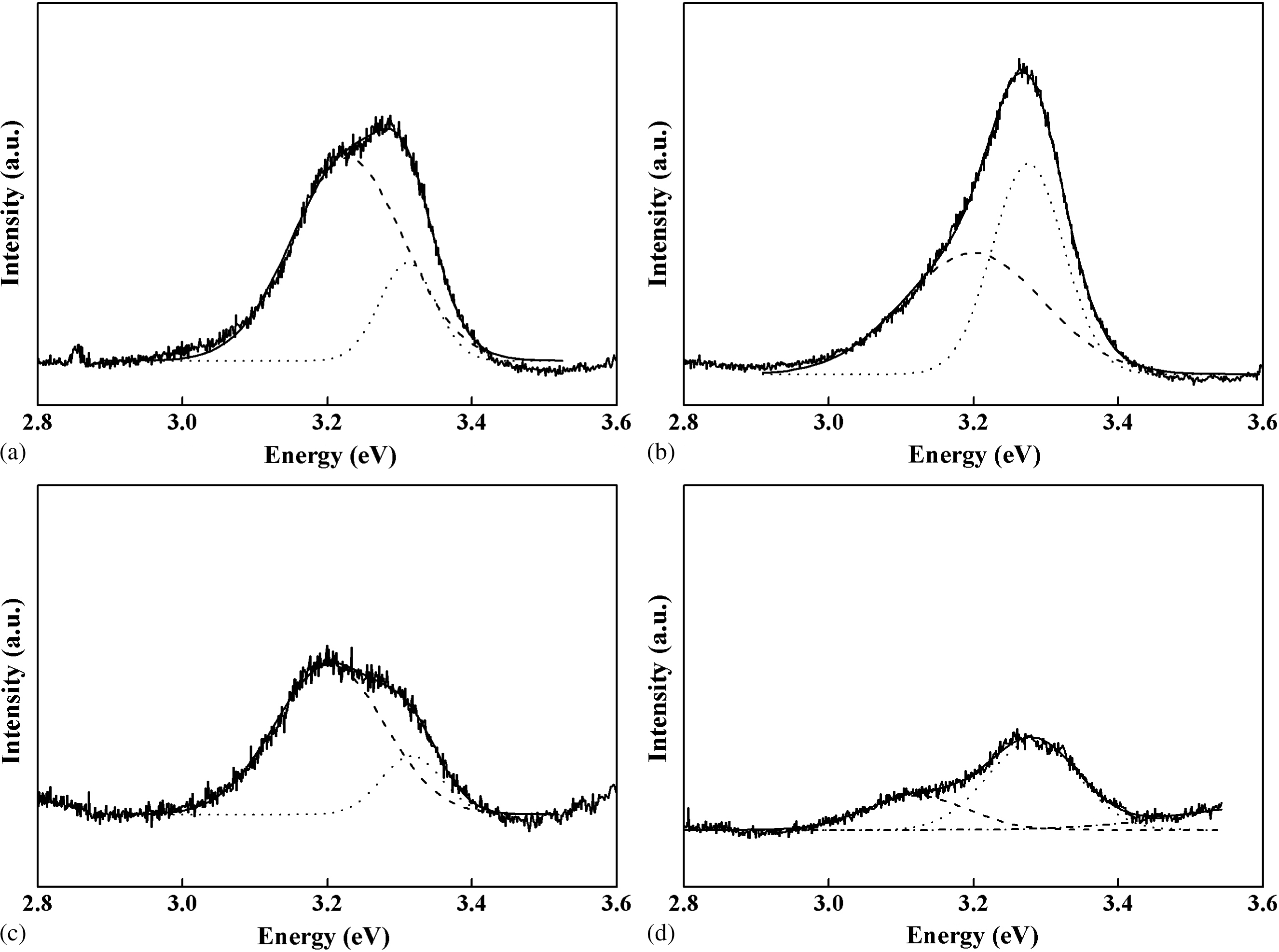
Photoluminescence spectrum of ZnO:P films with different Ar/O2 gas ratios measured at room temperature: a pure Ar; b Ar/O2 = 1/0·05; c Ar/O2 = 1/3; d pure O2
The low temperature optical properties of ZnO:P film obtained with Ar/O2 = 1/0·05 at 80 k is given in Fig. 5. It can be seen from Fig. 5, the PL peak appears at 3·345, 3·282 and 3·169 eV without any strong deep level emission. Deep level emission is known to be related to a variety of defects such as donor defect Zni, VO, acceptor defect Zn vacancy (VZn) and antisite defect O substitutional Zn (OZn).22,23 Compared with PL spectrum in other works, the PL spectrum of ZnO:P film with a peak at 3·345 eV can be attributed to neutral–acceptor bound exciton (A°X),10,24,25 and two other peaks at 3·282 and 3·169 eV can be attributed to donor–acceptor pair (DAP)26–28 and background peak respectively. Based on above results, the observed acceptor related PL emissions and hole concentration are related to the P dopant in the film. 13
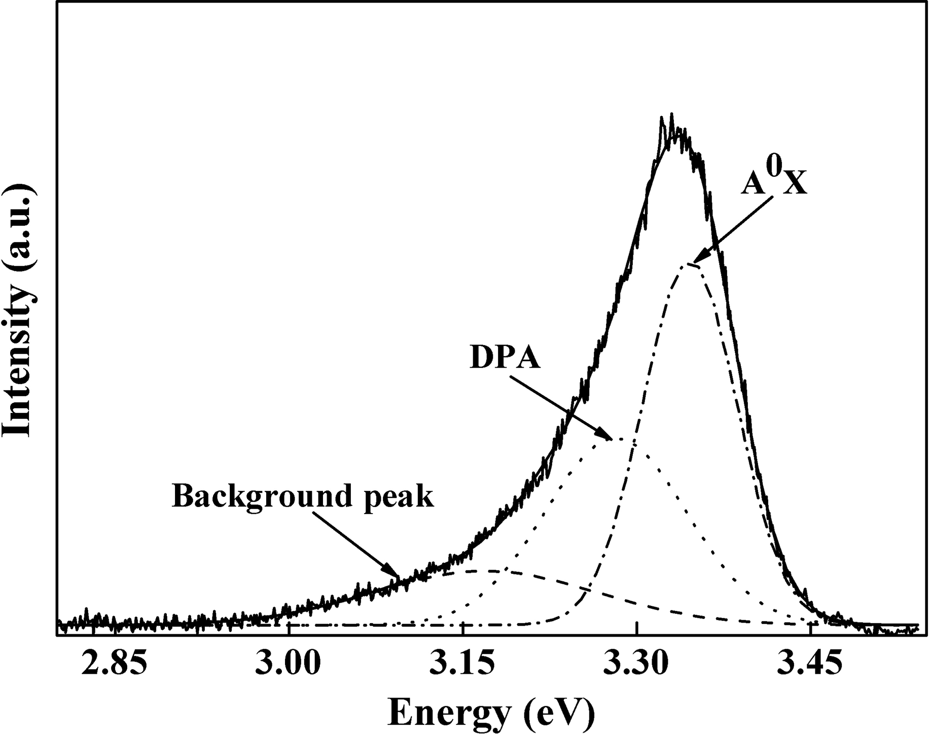
Low temperature PL spectrum of p-type ZnO:P film measured at 80 k
The acceptor energy of the P dopant is estimated from the DAP transition at 3·282 eV in PL spectrum of p type ZnO:P. The DAP energy is given by
28

 can be estimated by letting
 , with NA∼1017–1018 cm− 3, giving ΔE∼0·018–0·03 eV. At 80 k, the band gap is 3·437 eV and the donor energy is known to be ∼60 meV.1,29 Thus, EA ≈ 0·113∼0·125 eV. The high end of this range is comparable to the acceptor energy level of 127 meV in Hwang et al.
13
This value is nearly to the ionisation energy of PZn–2VZn (0·18 eV) as a shallow acceptor in ZnO:P film.
30
The total defect is like acceptor with an s transition at 0·18 eV above the valence band.
, with NA∼1017–1018 cm− 3, giving ΔE∼0·018–0·03 eV. At 80 k, the band gap is 3·437 eV and the donor energy is known to be ∼60 meV.1,29 Thus, EA ≈ 0·113∼0·125 eV. The high end of this range is comparable to the acceptor energy level of 127 meV in Hwang et al.
13
This value is nearly to the ionisation energy of PZn–2VZn (0·18 eV) as a shallow acceptor in ZnO:P film.
30
The total defect is like acceptor with an s transition at 0·18 eV above the valence band.
A ZnO homojunction was synthesised by depositing undoped n-ZnO layer on the P doped p-ZnO layer, and its I-V characterisation was investigated and shown in Fig. 6. Ni/Au and In metals were respectively used as p type and n type electrodes, which showed good ohmic characteristics after a thermal treatment, as shown in the inset of Fig. 6. As shown in Fig. 6, traditional rectifying behaviour can be measured in the ZnO p-n homojunction, indicating that the p-type ZnO:P can be applied to fabricate ZnO p-n homostructure LED. Further study is necessary to optimise and reveal the application of the p type ZnO:P as the surface coating in engineering field.
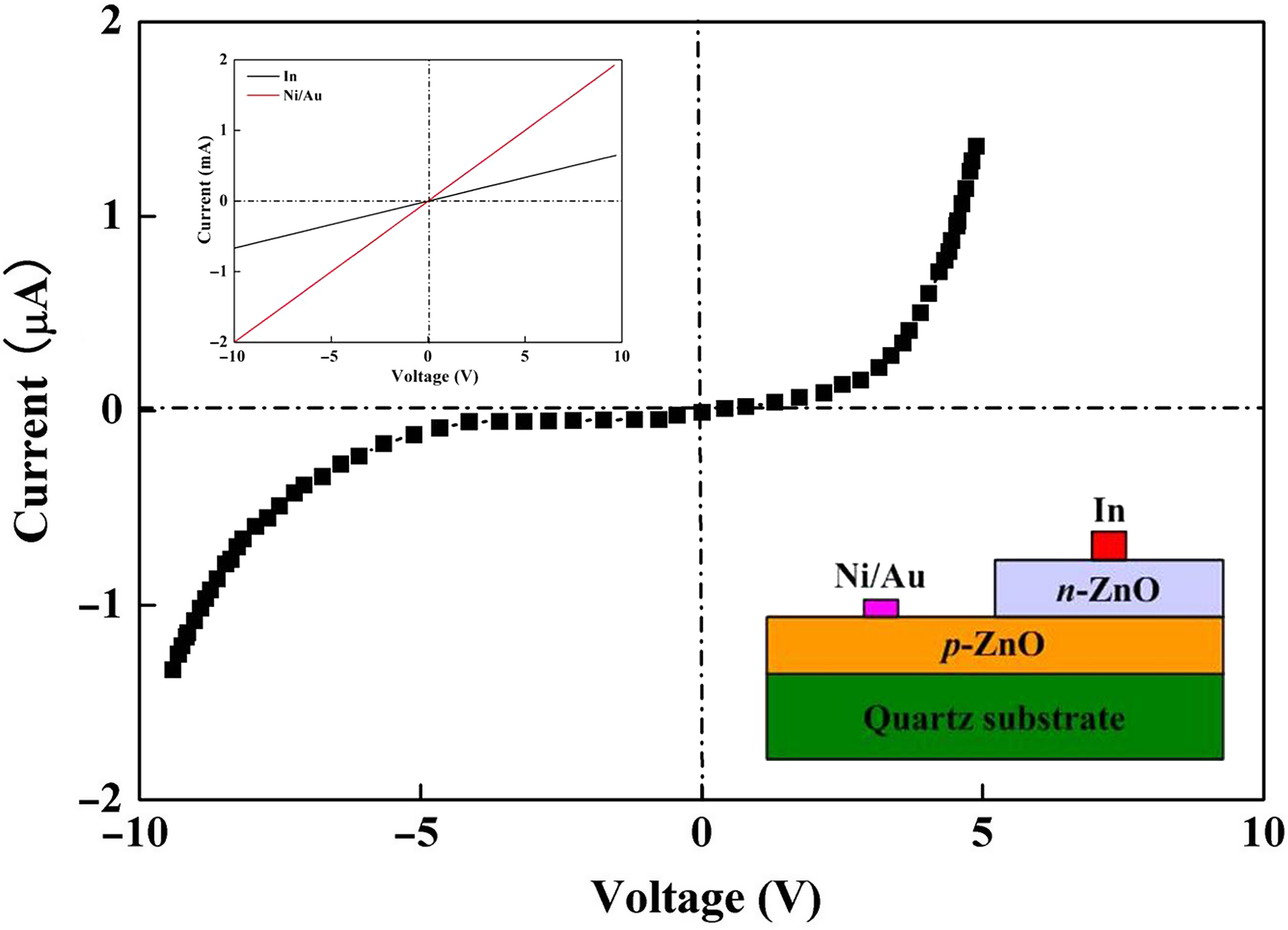
I-V characteristics of homojunction composed of undoped n type ZnO and p type ZnO:P. Upper left inset shows I-V characteristic of Ni/Au/p type ZnO contacts and In/n type ZnO contacts. Lower right inset shows schematic structure of p-n homojunction
Conclusion
In summary, p type ZnO:P film can be obtained with Ar/O2 = 1/0·05 after air RTA. The p type ZnO:P had a resistivity of 59·75∼59·86 Ωcm, a hole concentration of 2·34 × 1017∼2·11 × 1018 cm− 3 and a mobility of 0·05∼0·47 cm2 V− 1 s− 1 respectively. The PL spectrum peak at 3·345 eV corresponded to A°X of the p type ZnO:P film. The shallow acceptor energy level was estimated to be located at 113∼125 meV above the valence band. The formation mechanism of p type ZnO:P film was related to the PZn–2VZn complex acceptors. The p-n homojunction showed rectifying diode behaviour.
Acknowledgements
The authors acknowledge the financial support of National Natural Science Foundation of China (no. 11447194) and Jilin Institute of Chemical Technology Foundation for Science and Technology Plan Project (JLICT-2014112).