
Abstract
The accurate measurement of stress is an essential requirement of residual stress studying. In this paper, Cu thin films with different thickness were prepared by magnetron sputtering. The micromorphologies of the films were observed using atomic force microscopy, and the microstructures were analysed by transmission electron microscopy and X-ray diffraction. The residual stress distributions of the films were measured by the curvature and nanoindentation methods. The results show that Cu films present polycrystalline state, and the grains size grew up with increasing film thickness. The residual stress calculation results from nanoindentation tests using the Suresh model were consistent with the curvature method, the residual compressive stress changed into residual tensile stress and the D values (the difference between the maximum and minimum stress value) decreased with increasing film thickness, and the stress distribution became uniform. The interface stress of the films weakened with the film thickness increasing because the crystalline grains grew larger.
Introduction
The thin film materials with small volume and high reliability have become an integral part of microelectromechanical systems and have a wide range of applications in national defence, aerospace, communication, automobile manufacturing and other fields. The service reliability and service life are determined by the mechanical properties of thin film materials. 1 However, due to the difference in intrinsic properties between the film and the substrate, stress concentration and microdeformation of thin films often occur. The presence of residual stress will have a great influence on the mechanical properties such as static and fatigue strength, which leads to deformation, brittle fracture and stress corrosion cracking.2,3
The residual stresses can be measured by a range of methods such as X-ray diffraction (XRD), hole drilling, strain/curvature, 4 Raman spectroscopy, 5 ultrasonic 6 and magnetic methods. Owing to limitations of the thin film material itself, with these methods, it is difficult to measure the residual stresses non-destructively. The measurement by hole drilling method is destructive, Raman method is not very suitable for metallic thin films, and XRD method measures the residual stress in the substrate through the film for some thinner films in the nanometre range.7,8 The curvature method can measure the overall curvature of samples no matter whether the tester contacts the sample or not, and can calculate residual stress distribution in the sample. So, this method has the advantage of causing no damage to the original film, and it provides the average residual stress of the sample across the thickness.9,10
The nanoindentation technique, as a new type and effective tool for characterisation of material properties and mechanical behaviour in micro- and nanoscale, can not only obtain the material hardness, modulus of elasticity and other mechanical parameters but also reveal the microdeformation mechanism. The building of several residual stress calculation models, such as the Suresh model and Lee model, promotes the nanoindentation technology applied to the residual stress measurement.11,12 Zhu et al. measured the residual stress in quenched 1045 steel by nanoindentation method and XRD method, and the stress value calculated by the Suresh model was − 117 ± 20 MPa, which approaches the XRD result of − 114 ± 32 MPa. These results demonstrate that nanoindentation methods can be applied for experimental determination of residual stress.13,14
In a certain range of film thickness, the stresses are influenced by the thickness and the microstructure. In this paper, the nanoindentation test technology and optical phase shift technology are used to research on the internal residual stress evolution features of copper films with different thicknesses and to analyse the relevance of the microstructure and residual stress.
Experimental
Sample preparation
Four kinds of copper thin films with different thickness were deposited on the (100) silicon substrate of dimension Φ50 mm and NaCl substrate of dimension 10 × 10 mm by DC magnetron sputtering. The substrate was initially cleaned thoroughly with acetone in ultrasonic bath. After arranging the substrates, the chamber was evacuated using a turbo molecular pump, backed by a rotary pump up to a high vacuum ( ≤ 2 × 10− 4 Pa). After evacuation, an inert gas like argon (99·999% purity) was fed into the chamber via gas inlet valve. Ar gas pressure was 0·5 Pa. The DC bias was 20 V. The operating power is 0·4 kW, and the current of the sputtering source is 0·35 A. The sputtering target is a Cu target of dimension 360 × 80 × 10 mm with 99·9999% purity. Before sputtering, the substrates were cleaned by Ar ion for several minutes. The sputtering rate is 20 nm min− 1, and the chamber temperature is 200°C. The thicknesses of the samples were 100, 500, 1000 and 2000 nm. In addition, the deposition time corresponding to each thickness is 5, 25, 50°and 100 min.
Microstructure characterisation
Surface morphologies and roughness of films were examined using a Nanoscope Dimension atomic force microscope (AFM) operating in tapping mode. The microstructure and phase composition were investigated using transmission electron microscopy (TEM). In order to check the crystallinity of the films, XRD analysis was carried out with a diffractometer using Cu Kα1 (0·154056 nm) radiation at 30 kV and 25 mA. The films were scanned in the standard θ − 2θ geometry from 20° to 100° with a 0·05° step size and 30 s dwell time.
Curvature tests
The stress distribution of Cu films on the Si substrate was measured by a GS6341 electronic thin film stress distribution test instrument. The principle of laser interference phase shift was used to measure the changes of the curvature radius of a substrate before and after preparing the films respectively. Figure 1 shows the schematic layout of the system.
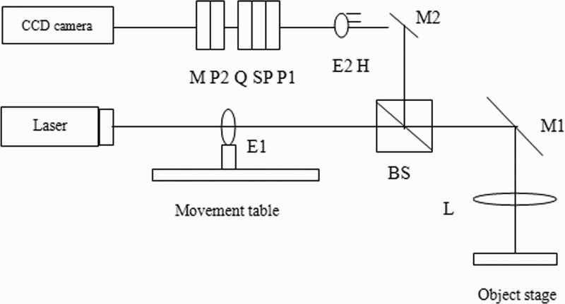
Schematic layout of electronic thin film stress distribution test instrument
The parameters in Fig. 1 are as follows: E1, expand beam glass; BS, beam splitter; M1, reflecting mirror; L, lens; M2, reflecting mirror; H, hole; E2, lens; P1, polarizer, SP, share mirror; Q, 1/4 retardation sheet; P2, polarization analyzer; M, mat glass.
The thin film stress value is calculated according to the Stoney equation.10,15
Nanoindentation tests
Nanoindentation tests were performed on the film surface using a Nano Indenter XP (MTS Corporation, USA) with a diamond Berkovich indenter. Depth control was adopted under peak indentation depths of 1/10 the film thickness. Continuous stiffness measurement module was selected, and the continuous changes of hardness and modulus with the indentation depth were obtained. Based on the Oliver–Pharr theory and the typical nanoindentation load–displacement curve, the hardness H and elastic modulus E can be calculated.16,17
In this paper, the Suresh model was chosen to calculate the residual stress based on the calculation of the difference between the indentation contact areas of stressed and unstressed samples by analysing the indentation load–depth data according to the following equations:
For tensile residual stress
Results
Surface morphology and roughness
Figure 2 shows the granular surface morphology of the Cu films with four different thicknesses by AFM. The films present grains of a regular shape like islands. The 100 nm thick film had the highest island density with an average size 65 nm and a roughness Rrms of 0·85 nm (Fig. 1a). With the increase of film thickness, the size of surface islands increased and the density decreased. For the 500 nm thick Cu film, the average diameter is ∼100 nm and the roughness is Rrms 1·83 nm (Fig. 1b). For the 1000 nm thick Cu film, the average diameter is ∼130 nm and the roughness is Rrms 4·04 nm (Fig. 1c). The average diameter and roughness for the 2000 nm thick Cu film are ∼230 nm and Rrms 13·1 nm (Fig. 1d). The surface granule grew in a vertical direction and presented dynamic coarsening behaviour with the increase of film thickness.
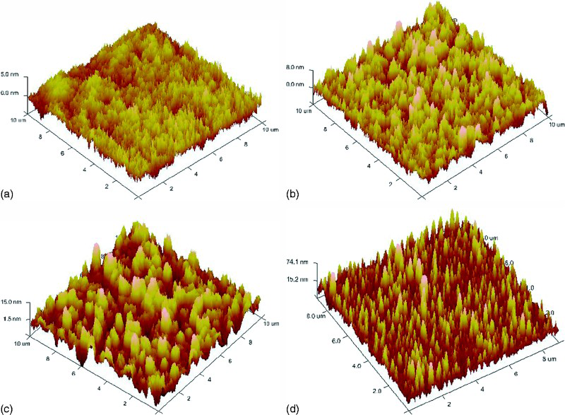
AFM characterisation of films with different thickness: a 100 nm; b 500 nm; c 1000 nm; d 2000 nm
Structural characterisation
Figure 3 shows the XRD analysis of Cu films. The reflections of (111), (200), (220) and (311) planes were found; (111) is the most intense plane. Because the crystalline structure of Cu is f.c.c., the (111) planes have the lowest surface free energy. The result is also consistent with the computation by Weihnacht and Bruckner. 18 The minimum of surface energy and interface energy plays a leading role and leads to (111) orientation of grain growth when the Cu film thickness is very thin. The diffraction peaks (111) and (200) increased with the increasing of film thickness, while the other diffraction peaks did not change as obviously as they did.
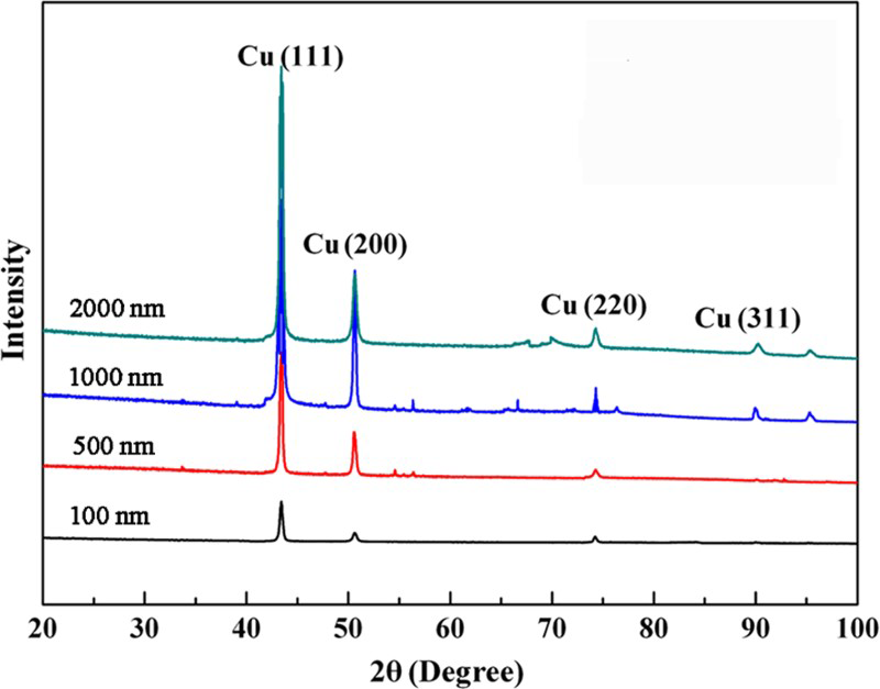
Phase structure of films with different thicknesses
Figure 4 shows the representative bright field image and the corresponding diffraction pattern for the four kinds of films by TEM. The films were polycrystalline with nanoscale grains. The grain size was uniform, and the grain boundary was obvious. The lattice parameters of the four kinds of films were similar and ∼2·00 Å. The grain diameter increased from ∼5 nm in the 100 nm thick film to ∼60 nm in the 2000 nm thick film. In addition, the quantity of the crystal grains increases with increasing film thickness. Moreover, the results of diffraction pattern calibration were consistent with the results of XRD measurements, film growth preferentially selected (111) crystal orientation. Therefore, the degree of crystallisation was influenced by thickness, but the growth of film crystal orientation was not affected. In addition, the surface islands do not consist of individual crystalline grains but contain clusters of crystals in the AFM maps.
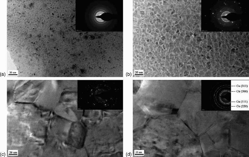
Bright field image and corresponding SAED map for 2000 nm thick film
Mechanical properties
The samples were typical soft film/hard substrate material couples, so the measured result of hardness by nanoindentation would be larger than the true value due to the existence of the substrate. The hardness and elastic modulus of the films were measured by continuous stiffness measurement (CMS) technology. Figure 5 shows the hardness–depth curves of the films deposited onto the Si substrate. The curve had three stages in Fig. 5a: in the 0–8 nm of the depth, the hardness decreased with the indentation depth increasing, because the film material is in the elastic deformation stage and a size effect exists. Between the 8 and 15 nm depth, the film in the elastic deformation stage, the hardness value changed slowly and attained a hardness of 1·85 GPa. The material was still in the elastic deformation stage, but the size effect became weakened. When the depth was larger than 35 nm, the hardness of the film increased gradually with indentation depth increasing. The material began to deform plastically, and the influence of substrate increased. Similarly, the hardness values of 500, 1000 and 2000 nm thick films were 1·95, 2·4 and 2·5 GPa. Figure 6 shows the modulus–depth curves of the films with the Si substrate by CMS. The modulus values of 100, 500, 1000 and 2000 nm thick films were 114, 119, 135 and 139 GPa. The change tendency of the hardness and modulus with increasing film thickness was similar.
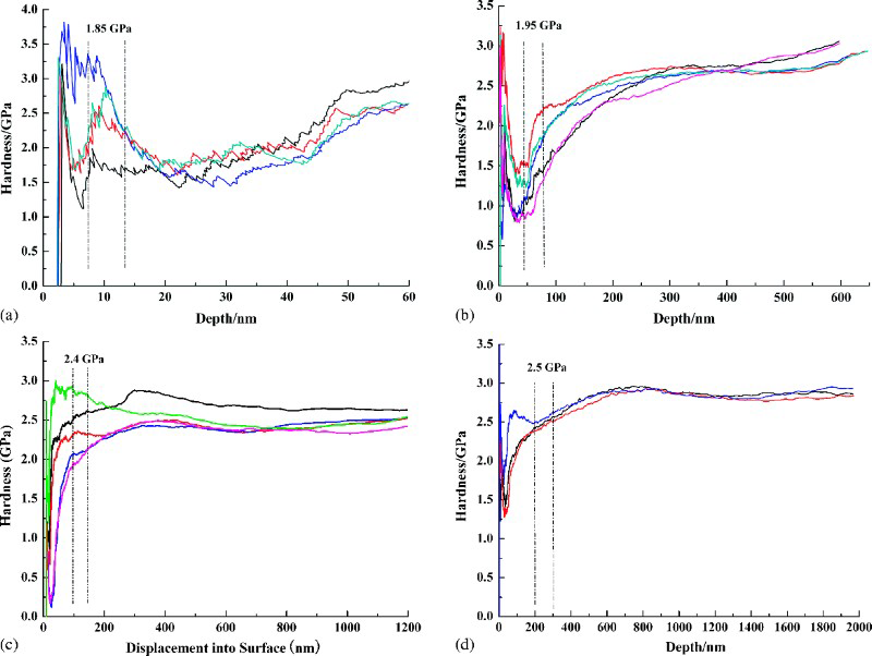
Hardness versus displacement curves of Cu films: a 100 nm; b 500 nm; c 1000 nm; d 2000 nm
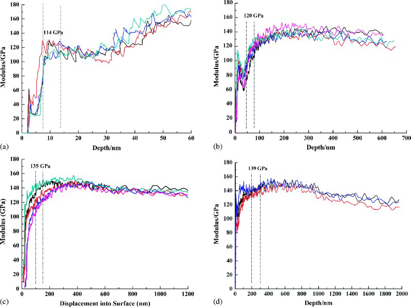
Modulus versus displacement curves of Cu films: a 100 nm; b 500 nm; c 1000 nm; d 2000 nm
Residual stress
Figure 7 shows the three-dimensional stress distribution images of the Cu films with four different thicknesses, which were measured with the measurement dimension of Φ44·5 mm by electronic thin film stress distribution test instrument. The average stress Savg, the maximum stress Smax and minimum stress value Smin are listed in Table 1.
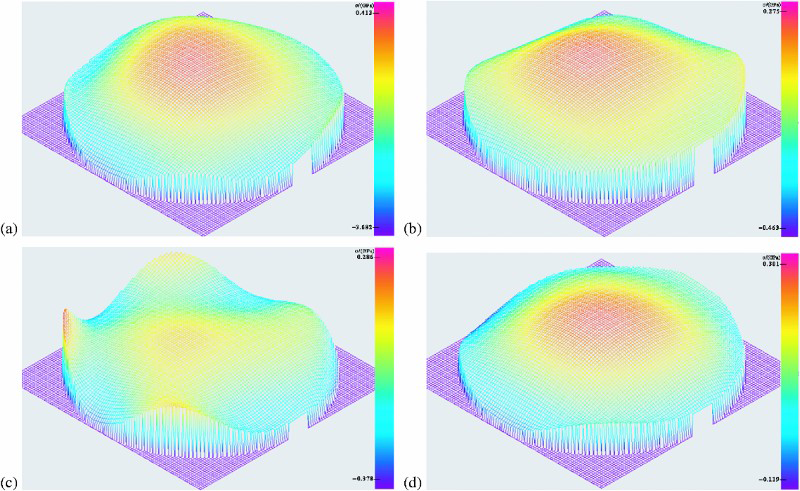
Three-dimensional stress distribution image of different thickness Cu films: a 100 nm; b 500 nm; c 1000 nm; d 2000 nm
Residual stress of films with different thickness
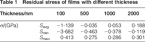
The stress in the 100 and 500 nm thick films was compressive, whereas it was tensile in the centre area of 1000 and 2000 nm thick films. The average stress of Cu film increased with increasing films thickness, changed from compressive stress to tensile stress, with the distribution range of ∼ − 1·139 to 0·188 GPa. Stress D value (the difference between the maximum and minimum stress) decreased with the film thickness increasing; thus, the stress distribution of Cu films became uniform with the increase of film thickness.
Figure 8 shows the typical load–depth curves of the stress free and stressed samples. The penetration depths of 1000 and 2000 nm thick films were 100 and 200 nm. As the deformation of the metal thin film is susceptible to the substrate during the loading process, it is generally considered that, when the indentation depth is 1/10–1/7 of thickness of the film, the substrate has a smaller influence on the measured hardness values. 19 So, the mechanical property of the 100 and 500 nm thick films was measured using CMS.
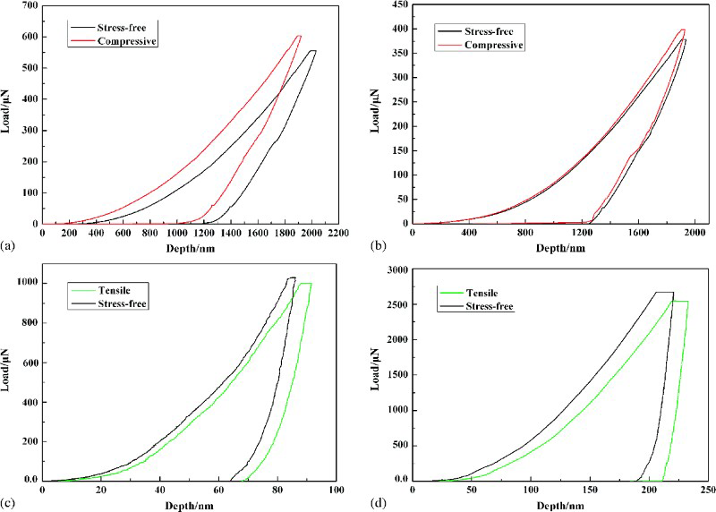
Typical load–depth curves of stress free and stressed samples: a 100 nm; b 500 nm; c 1000 nm; d: 2000 nm
The stressed samples of 100 and 500 nm thick films had a larger peak load and elastic recovery after unloading than stress free sample, so there should be internal compressive stress in them. However, there was residual tensile stress in the 1000 and 2000 nm thick films. Calculated by the Suresh model, the residual stresses of 100, 500, 1000 and 2000 nm thick films were − 0·984, − 0·057, 0·083 and 0·136 GPa respectively. The calculation results were between the maximum and minimum values of stress measured by curvature method; thus, the residual stress can be accurately measured by nanoindentation method. The percentage error was < 13·6%, and it was in an acceptable range.
Discussion
According to the position and formation process of the intrinsic stress, the intrinsic stress consists of interface stress and growth stress. 20 The mismatch of film and substrate due to their different coefficients of thermal expansion will create interface stress, and the growth stress originates from the structure defects during the growth process. If there is a large difference between film and substrate or quite high density of defects and impurities, this would cause serious interface mismatch and lead to extremely large interface stress. While the interface stress is very large and the growth stress contribution is very small, the average intrinsic stress would decrease with increasing film thickness. Owing to the big interface stress, the residual stress of 100 and 500 nm thick Cu films put up decrease tendency with the film thickness increasing. While the thickness increased to a definite value, the interface stress plays an unimportant role in the whole residual stress.21,22
The uniformity of the film surface decreased as the thickness of the films continued to increase, such as the 1000 and 2000 nm thick Cu films. The surface shapes were observed by electronic thin film stress distribution test instrument, and the thickness of the films is inhomogeneous. This resulted in the inner residual stress gradually changing into tensile stress and slowly increasing.
The thickness of the film plays an important role in the influence of the residual stress, as well as the microstructure of the films. There were obvious differences between the microstructures of Cu films with different thicknesses, which also have a great influence on the film stresses. Figure 4 shows the TEM images of Cu films of different thicknesses: the Cu thin films were polycrystalline and the phase structure did not change with the thickness increasing, and the crystal structure was still face centred cubic. There was a lower crystallisation degree and smaller grains in the thinner films, and they both increase with increasing film thickness. Therefore, the Cu film crystallisation was getting better and better with the film thickness increasing.
The changes of Cu film microstructure with thickness showed that there were lattice defects and a lot of small grains in the thinner films. Compared with bulk materials, the grains of thin films have larger specific surface area. With the film thickness increasing, the grains grew and the lattice defects decreased. 20 The enhancement of diffraction intensity showed that the recrystallisation was enhanced, and grain boundary diffusion promoted grain growth. Thus, the grain specific surface area was smaller and the tensile stress increases (see Table 1). The crystal lattice mismatch and the high density of defects were reduced at the interface between the film and substrate, and the grains grew gradually. Thus, the interface stress was reduced, leading to relaxation of residual stress and reduced compressive stress. Therefore, microstructures of films play an important role on the film stress state.
Conclusion
The nanohardness and elastic modulus of Cu films of different thickness were extracted by nanoindentation tests using the CSM method, and the residual stress values were calculated from the same nanoindentation tests by the Suresh model. The stress values were reduced in modulus and changed from compressive to tensile with increasing thickness, and the internal stress difference value was also decreased. The influence of the interface stress decreased, but the roughness also increased and uniformity decreased as the films thickness continued increasing. The grain grew and defects reduced with the film thickness increasing, and the Cu film crystallisation was getting better and better. In addition, the crystal lattice mismatch and high density of defects were reduced at the interface between the film and substrate. This lead to the relaxation of residual stress and reduced the internal residual stress. Therefore, the sign of residual stress within a small area of film can be qualitatively reflected by nanoindentation method.
Footnotes
Acknowledgements
This paper was financially supported by NSF of Beijing (grant no. 3120001), 973 Project (grant no. 2011CB013405), NSFC (grant no. 51275105) and Fundamental Research Funds for the Central Universities (grant no. HEUCF).