
Abstract
The present work focuses on characterisation of the deposited layer on aluminium substrate processed with electric discharge coating process. Different characterisation techniques such as scanning electron microscopy, energy dispersive X-ray and X-ray diffraction (XRD) have been employed to study the surface morphological changes, presence of materials and their phase transformations due to the formation and deposition of composite material layer on work surface. The grain size of the deposited particles has a significant effect on mechanical properties. Thus, an attempt has been made to calculate the grain size, dislocation density and microstrain of deposited material and its particles. The formation of tungsten carbides, namely, WC and W2C, is detected through XRD analysis. Clusters of globular particles in nanoscale are observed throughout the deposited layer.
Introduction
Electric discharge machining (EDM) has emerged as a powerful modern manufacturing process from the last few decades. Typical applications include in the area of dies and press tools industries, automotive and aerospace. EDM has the capabilities of machining any hard material that is electrically and thermally conductive. Attempts have been put forwarded by some researchers to machine non-conductive materials with EDM by coating substrate surface with conductive material. 1 EDM has opened the door for another area of research in the line of surface modification. The modification of substrate surface using EDM is popularly known as electric discharge coating (EDC). This process has the capabilities of producing thick and thin layer coating on the work surface by simply varying process parameters. It develops a protective layer that is harder, tougher, corrosion resistant and heat sensitive than the base material in a particular shape on a specific portion of a part.2,3 EDC can also be used to texture the rolls 4 and in fixing damaged regions,2,3 which indeed increase durability of a part. EDC process can be used to deposit a composite layer on the surface of the cutting tools, moulds 5 and drills 6 to lengthen their life. It can also find application in the field of the surface repairing and strengthening of components. 5
The modification of a work surface in EDC process can be achieved by two methods. The first method involves adding powder particles of desired materials to be deposited in the dielectric fluid, and the second method involves the use of powder metallurgical (PM) electrodes. Both these methods deposit materials on the work surface whenever spark occurs between the electrode and workpiece. The present work uses the second method of depositing material on the work surface.
Various researchers have investigated the influence of process parameters that affect the EDC process. Chen et al. 3 have conducted dry EDC for modifying the surface of Al alloy substrate using titanium PM compact electrodes in the atmosphere of nitrogen gas. The deposition of TiN on the substrate surface has been observed. Mussada and Patowari 7 also succeeded in employing Taguchi approach to deposit a composite layer of W and its carbides using W–Cu PM electrodes on the surface of mild steel and later conducted a detailed investigation of EDM parametric effects of the deposition process. 8 Naveen et al. 9 attempted to optimise EDC parameters in Taguchi routes and succeeded in depositing a composite layer of Fe2W3C6 on Inconel 718 using W–Cu PM electrodes.
After conscientious literature survey, it can be inferred that no researcher has yet attempted to calculate the grain size of the deposited material. It was a guess that the deposition using PM electrodes in EDM may lead to nano- or microdeposition. In the present experimental investigation, efforts have been made to deposit a hard uniform layer consisting of tungsten and its carbide on soft aluminium substrate. Applying characterisation techniques like scanning electron microscopy (SEM), energy dispersive X-ray (EDX) and X-ray diffraction (XRD) to study morphology, the presence of elements detected phases present in the deposited layer. An attempt has been made to calculate grain size, dislocation density and microstrain of the deposited particles.
Experimental
The conventional die sinking electric discharge machine is used for EDC process. Reverse polarity is selected as it supports the deposition process, and flushing pressure is maintained at 5 kg cm(2. The process materials and parameters with their levels selected for the experimentation are given in Table 1. The on time and off time values are selected such that the duty factor is maintained within 0·5–0·7. The present work utilises EDC process to deposit a hard layer of tungsten and its carbide on the surface of soft materials like aluminium. Hence, W powder of 325 mesh size is selected for tool material, and adding Cu to it enhances electrical conductivity. This combination boosts the sparking phenomenon and results in high material transfer rate (MTR). Hydrocarbon oil serves as a dielectric fluid. It is anticipated that hydrocarbon oil liberates carbon at the time of electric discharge, and this carbon reacts with tungsten to form tungsten carbide. Thereby, tungsten and its carbide get deposited on the substrate surface.
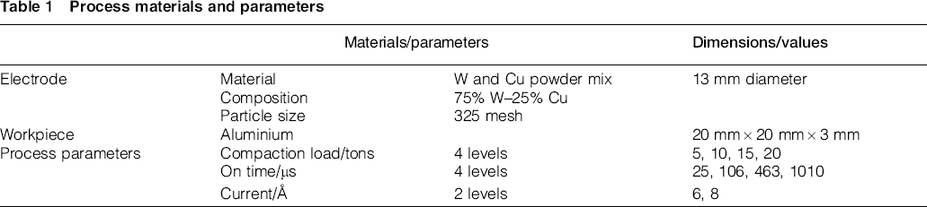
Process materials and parameters
Results and discussion
Experiments have been conducted with all the selected parameters and materials. MTR ranging from 22·24 to 171·72 mg min− 1 and layer thickness ranging from 77·31 to 816·72 μm have been deposited on the surface of aluminium. Thermal energy is generated between the tool and workpiece due to the formation of plasma channel, and the temperature rise is in the range of 8000–12 000°C 10 or as high as 20 000°C. This discharge energy melts some portion of electrode and workpiece material. At this stage, reaction between various elements, such as W, Cu, Al and C, from hydrocarbon dielectric fluid takes place. Some amount of molten metal is deposited on the workpiece, and the remaining is carried away by dielectric fluid. It is observed that layer thickness is increasing with increase in on time and current but is reducing with increase in compaction load. The previous work on calculating hardness indicates that the hardness of the deposited layer on mild steel is in the range of 576·7–1298·4 HV. 8 Different aspects related to characterisation of deposited layer are addressed in the following sections. The sequence of steps followed for deposition and characterisation of the deposited layer is shown in Fig. 1.
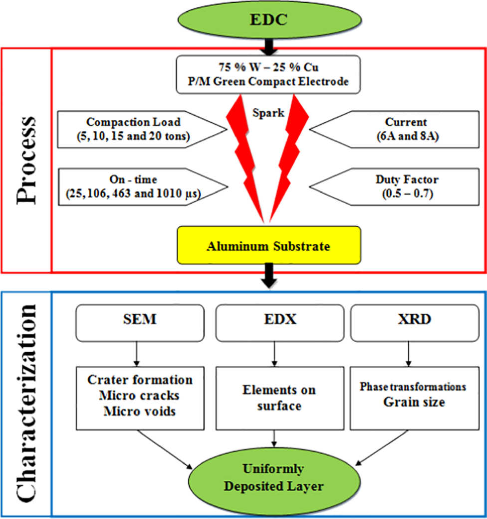
Sequential steps followed for deposition and characterisation of deposited layer
Optical microscopy and surface roughness
To observe the surface texture of a deposited layer, micrographs have been captured using a Leica DM 2500M optical microscope. The surface textures of some distinctive samples are shown as micrographs in Fig. 2a and b. The corresponding surface roughness profiles are also shown in Fig. 2c and d. At low on time and current levels, the material deposition is uniform throughout the substrate surface. For example, a sample processed with lower on time (25 μs) and current (6Å) produces a uniform layer of deposition. At high on time and current levels, the material deposition is uniform but the sample is quite rougher. For example, a sample processed with 106 μs on time and 8Å current produces a uniform and rougher deposition. With higher on time and current, high discharge energy channel is generated for longer duration between tool and workpiece, which melts larger portion of tool materials. The melted materials get dislodged from the electrode and deposit randomly throughout the work surface. This increases MTR and the surface roughness of the deposited layer.
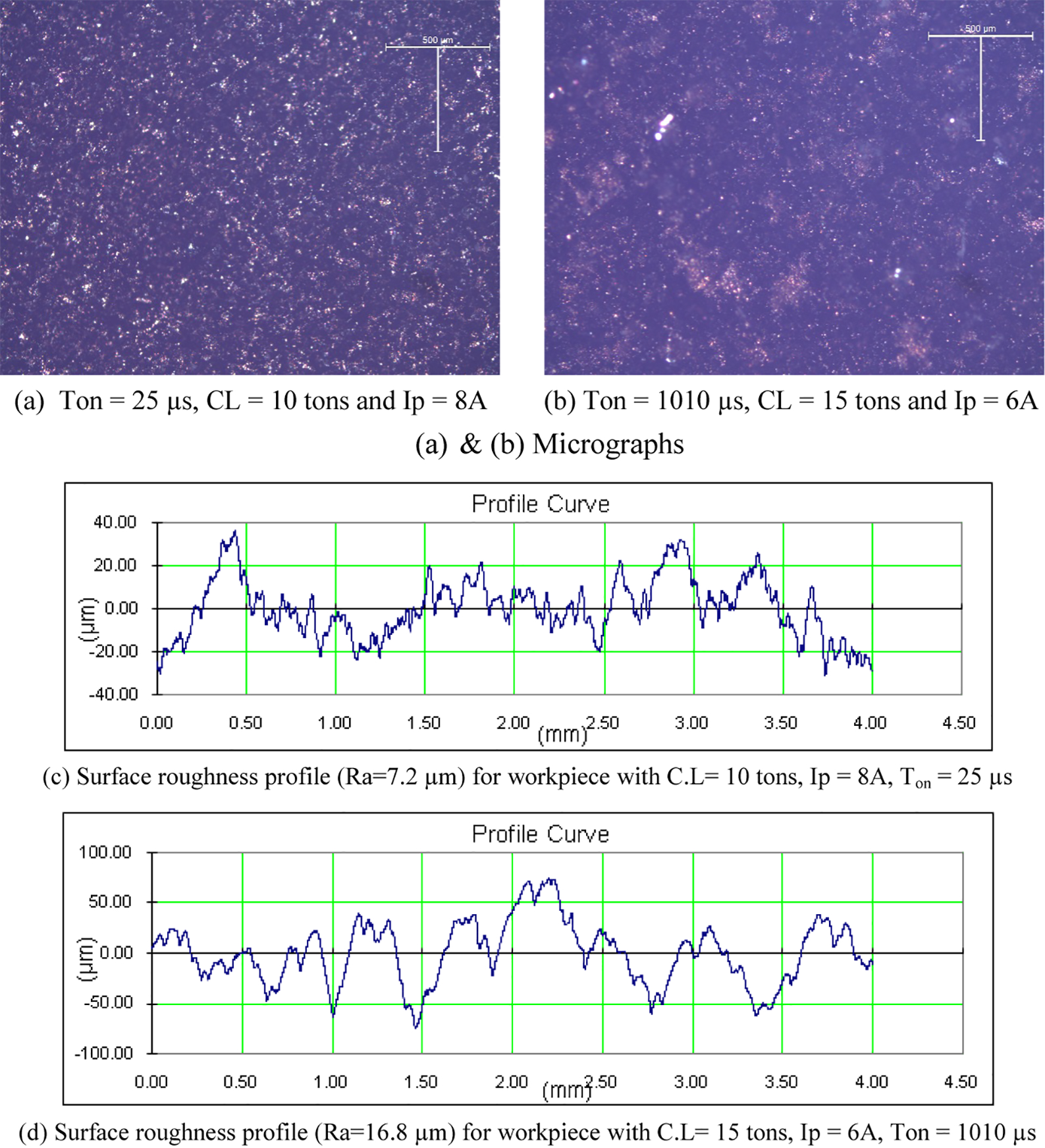
Optical micrographs and surface roughness profiles of deposited layer
Scanning electron microscopy
SEM analysis is performed to observe the morphological changes that occurred on work surfaces after EDC. SEM images at higher magnifications of the deposited layer on the samples processed with different parametric combination are captured and shown in Fig. 3. It is evident from these SEM images that the material is deposited on the substrate surface in globular forms with some volcanic features. Moreover, craters are also formed on the deposited surface because of subsequent sparking even after deposition.
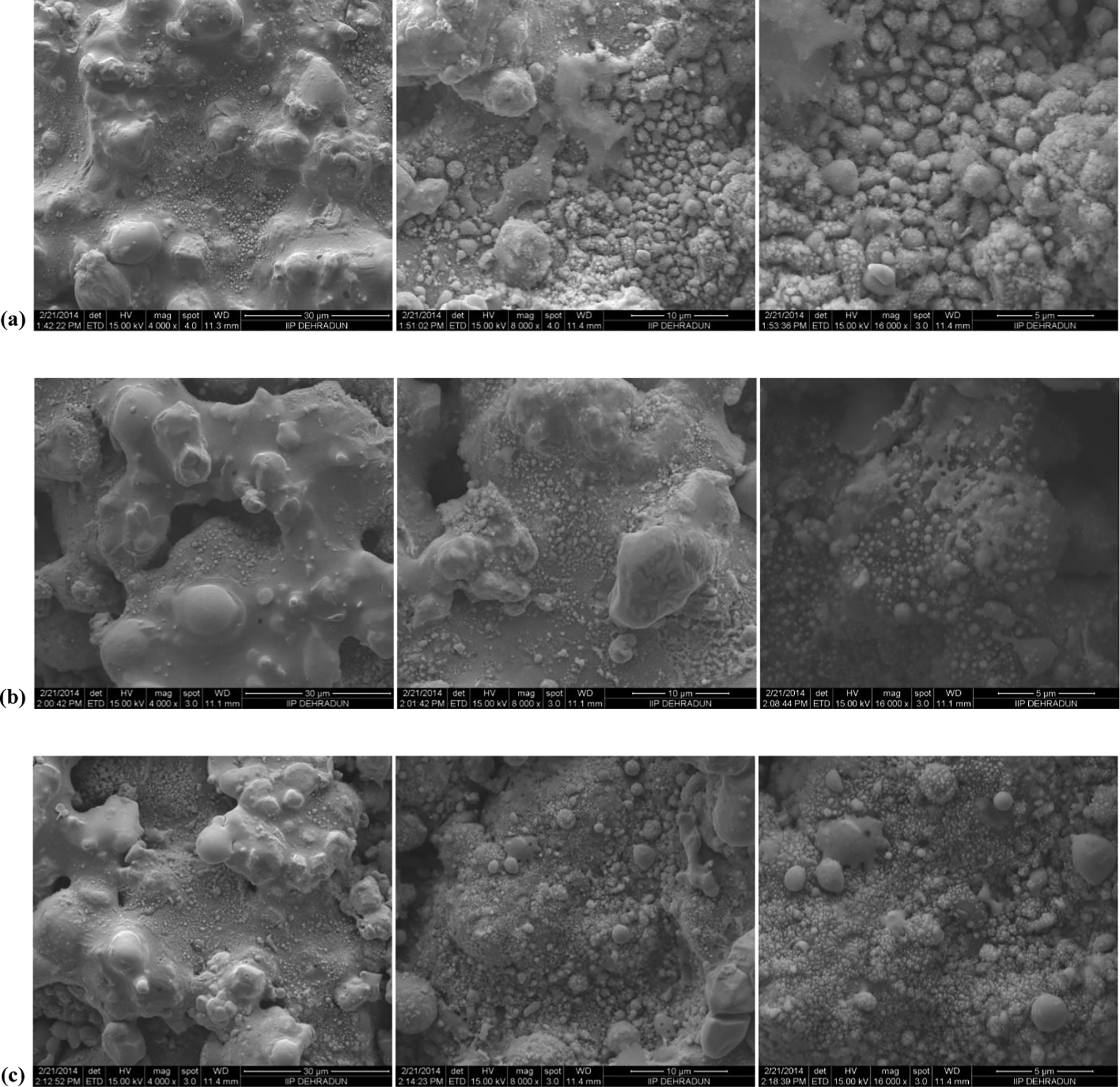
SEM of top layer of aluminium after machining with tungsten copper PM electrodes at 4000 × , 8000 × and 16 000 × : a CL = 10 tons, Ton = 106 μs and Ip = 8 A; b CL = 15 tons, Ton = 106 μs and Ip = 8 A; c CL = 20 tons, Ton = 106 μs and Ip = 8 A
SEM images infer that the material deposits on work surface layer by layer. In EDC process, pulsating current and voltage are used and every cycle has the pulse on time and pulse off time. Commonly, on time is referred as pulse duration and off time is referred as the pulse interval. The machining takes place for the period of pulse duration. At this time, tool materials get dislodged from the electrode and get deposited on the surface of substrate. In pulse interval period, the discharge diminishes and the supply of energy is arrested. Hence, in this period, the material transfer is ceased and there is no deposition of material, but the removal of debris and rapid cooling of the deposited layer takes place owing to flushing of dielectric. Owing to rapid cooling, deposited layer gets solidified faster. On this solidified layer, material gets deposited again in subsequent pulse duration. Removal of debris and rapid cooling takes place again in pulse interval period in cyclic order. This process is continuous throughout the machining time, and net amount of material gets deposited on the substrate surface layer by layer.
It can be noticed from Fig. 3a that the material is deposited uniformly on the substrate surface with very little depth variation. Globular deposition has been observed with perfect visibility of grain boundary separation throughout the deposited surface. The reason behind this form of deposition is that due to lesser compaction load (10 tons), the powder particles are loosely packed compared to that at higher compaction loads (15 and 20 tons). Whenever the discharge occurs, the materials from loosely packed electrodes freely flow to work surface, which not only increases MTR but also results in uniform deposition. Because of sufficient amount of transferred material, the interparticle space is filled up that makes the surface much uniform.
At the intermediate compaction load of 15 tons, the material is deposited uniformly on the substrate surface but with deeper variation compared to that of 10 tons. SEM image of the sample processed with electrodes of 15 ton compaction load is shown in Fig. 3b. The globules that formed in this case are of smaller diameter than that of the sample machined using CL of 10 tons. The increase in compaction load increases binding strength of powder particles and reduces the flow of tool materials and also the lump deposition. This may be credited to less localise melting of electrode material, which deposits materials randomly throughout the work surface. This results in generation of deeper voids in between the globules. Thus, it enhances the surface roughness. This can be observed very clearly in Fig. 3b at 4000 × magnification.
In Fig. 3c, SEM images of the sample machined using the tool compacted at CL of 20 tons is shown at different magnifications. At this high compaction load, there is a very less amount of material that is transferred to the work surface compared to the cases with lower compaction loads. The melting and vapourisation are restricted to a very narrow zone, which deposits molten material on work surface very irregularly. This irregularity of deposition results in formation of very deep voids in between the globules of deposited materials. Globular particles formed in this case have lesser diameter than that of samples machined using CL 10 and 15 tons. The reduction in size of globular particles may be attributed to non-occurrence of lump deposition.
Cracks and voids formation
Crack formation is one of the prominent surface defects that reduce resistance of material and increase corrosion and probabilities of fatigue failure. Two types of stress are present in the surface after machining process, i.e. thermal stress and tensile stress within. Thermal stress may be due to extreme heating and sudden cooling, which cause non-uniform distribution within the workpiece. 11 The complete removal of debris from the component surface is not possible by the dielectric. The parent material will contract less when compared with the molten material due to the diffusion of carbon into molten metal. Cracks will be formed when these stresses surpass the ultimate tensile strength.11–13 The cracks that formed on the top layer of the surface when machined with EDC process are shown in Fig. 4. It is observed that the surface cracks are formed on the deposited layer in the order of 1–2 μm in length.
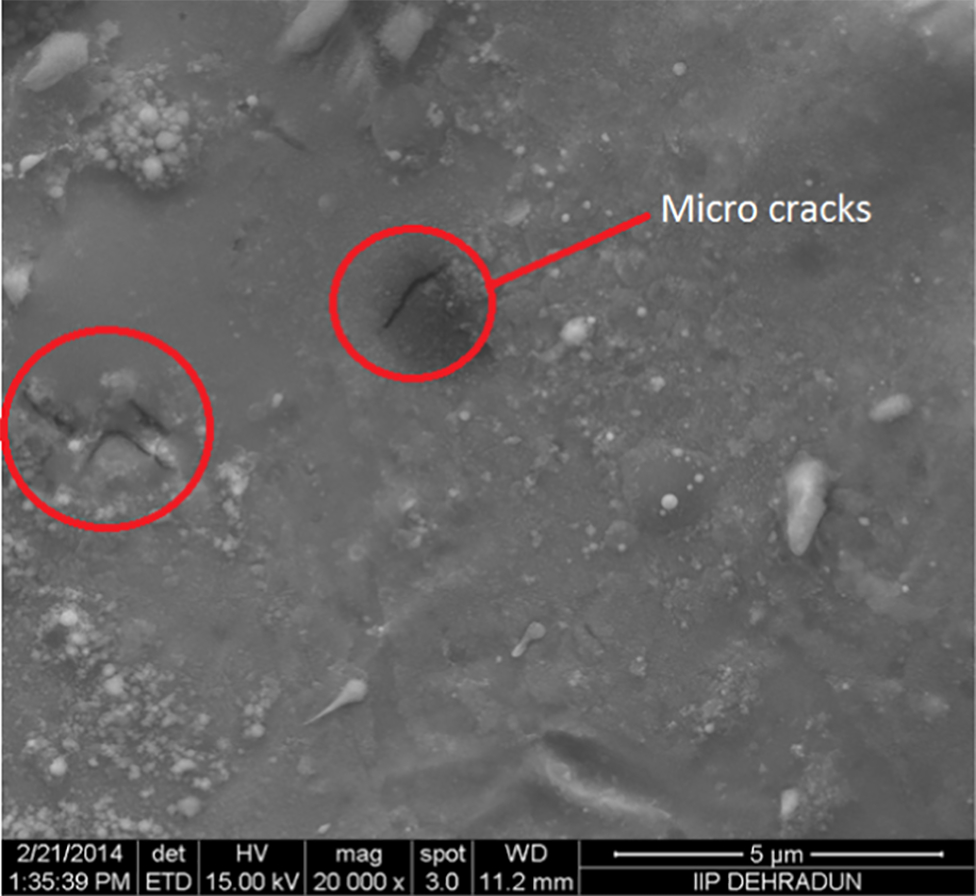
Microcrack formation on top layer of aluminium after machining with tungsten copper PM electrodes
Energy dispersive X-ray
EDX analysis is carried out to find the existence of elements in the deposited layer. The EDX micrograph of a sample is shown in Fig. 5. The existence of W, Cu, Al and C in the deposited layer is observed. Tungsten and copper have been observed as the main elements present in several EDX profiles. The presence of carbon is observed because of liberation of carbon particles and getting deposited on the work surface by forming the carbides of tungsten. The carbon is liberated from hydrocarbon oil, which is used as dielectric fluid in this experimental study. Aluminium is the substrate material so the presence of the aluminium is also observed in the EDX profiles.
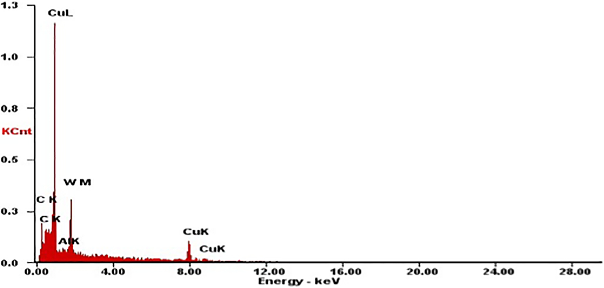
EDX profile of deposited sample machined at CL = 5 A, Ton = 106 μs and Ip = 6 A
XRD analysis
XRD is an efficient analytical method used for phase recognition of a crystalline material. XRD is performed on the deposited layer to detect phase transformations. X-pert Highscore plus software is used to analyse the XRD pattern, and using ICDD-Powder diffraction pattern, different elements and phase transformations have been identified. The presence of elements such as W, Cu and Al in addition to carbides of W such as WC and W2C in the deposited layer can be seen in XRD plot as shown in Fig. 6. Owing to the discharge energy, a chemical reaction occurs between W and carbon liberated from the hydrocarbon oil and deposits WC and W2C on the substrate surface.
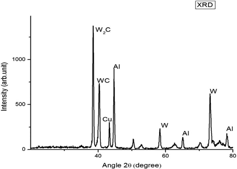
XRD diffraction peaks showing presence of W2C, W, Cu and Al on top layer of deposited surface
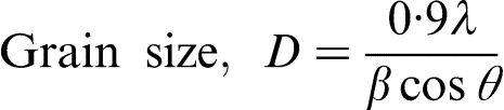
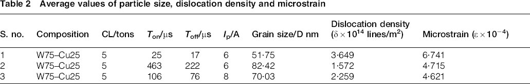
Grain size
Grain size (D) is an important parameter that influences mechanical properties such as hardness and toughness of an engineering material. To study the influence of grain size on mechanical properties, an attempt has been made to calculate the grain size of deposited materials after performing EDC process. For this, Scherrer's formula is used to calculate grain size (D) and is given by equation (1).
14
The values of the full width at half of the peak maximum (β) and Bragg's angle (θ) are identified for wavelength (λ) from XRD profile for every peak and substituted in equation (1) to find the grain size. The calculations are performed for every peak in the XRD profile, and average values are calculated. Grain size calculated using the Scherrer's formula confirms that the deposited particles are in the range of nanometers. It is observed that particle size is increasing with an increase in on time and current as given in Table 2. The EDC produces nanoparticle deposition that is very much comparable with other deposition processes such as chemical vapour deposition and physical vapour deposition.
Average values of particle size, dislocation density and microstrain
SEM images signify the presence of adjacent grains having different orientations with common grain boundary. These grain boundaries act as barriers for the dislocation movement. In other words, barrier strength increases with increase in disorientation of grains and grain boundaries. It may be noted that the smaller grain size increases the barrier tendency for slip phenomenon, which makes the material harder and stronger. This strengthening of materials by grain size refinement can be represented by Hall–Petch relation
15
and is given by equation (2). This relation specifies that the yield strength has an inverse square root relation with grain size (D). If the grain size is in nanometers, then the material attains superior yield strength values. It may be noted that finer grain size improves not only strength but also toughness.
Dislocation density and microstrain
Dislocation density (δ) is a count of dislocations in a quantity of material. Numerous features of dislocations are significant with respect to the mechanical properties of materials. These include microstrain (ϵ) fields that exist nearby dislocations, which are significant in identifying the movement of the dislocations. An attempt has been made to calculate the dislocation density and microstrain existence in the deposited layer on aluminium substrate using equations (3) and (4).
14
Conclusions
In this experimental investigation, EDC, which is a feasible and effective deposition process, was employed to modify the surface of aluminium. This study evaluates the characteristics of the deposited layer by performing roughness measurement, optical microscopy, SEM, EDX and XRD. It is observed that the surface roughness increases significantly with an increase in on time and current but very marginally with compaction load. The increase in current and on time deposits thicker layer with deeper voids. Moreover, craters are also formed on the deposited surface because of subsequent sparking even after deposition. It is evident from these SEM images that the material has been deposited uniformly on the substrate surface with discrete voids, craters and some volcanic features. The samples processed with low on time and current generate a uniform and thin deposition, but samples machined with high on time and current generate deeper irregularities in the deposited layer.
Composite layer enriched with W, Cu, Al, WC and W2C has been deposited on the surface of aluminium. Deposited particles have globular structures that are distributed throughout the deposition on work surface. The grain size of deposited particles has been calculated using Scherrer's formula. The present study serves as a proof that EDC leads to nanoscale deposition and average grain size achieved is of the order 51·75–82·42 nm. The effect of grain size, dislocation density and microstrain on mechanical properties such as strength, hardness, toughness and ductility has been examined and found that by varying EDC parameters, these mechanical properties can be controlled.