
Abstract
Two-dimensional graphene-like molybdenum disulphide with many unique properties, a relatively new and exciting transition metal dichalcogenide, has been extensively researched. This review discusses preparing molybdenum disulphide by vapour deposition, which has many advantages, including good spreadability, film uniformity and strong bonding forces with the substrate. We also review the compositing, decorating and doping of MoS2 by vapour deposition, and briefly discuss the applications of MoS2 produced by vapour deposition.
Introduction
Recently, graphene, a two-dimensional (2D) material, has attracted significant interest because of its unique electronic, optical and mechanical properties.1–3 Graphene is an excellent light to current converter with quantum efficiency close to 100%, owing to its long mean free path and high Fermi velocity. The layered and arrayed structure of graphene makes it ideal for high speed transistors and integrated circuits that consume less energy than conventional silicon electronics. However, graphene has no band gap, limiting its application in nanoelectronics and optoelectronics.4–6
Molybdenum disulphide (MoS2) is a naturally forming layered transition metal dichalcogenide. It is a silvery black crystal whose appearances and feels are similar to graphite crystals. Molybdenum disulphide also has similar properties to graphene, such as high carrier mobility, good toughness and ultra low thickness, except a stratified structure. However, MoS2 as a semiconductor has more advantages than graphene, such as a tuneable band gap (1·2–1·9 eV) and good light absorption.7–12 Molybdenum disulphide has received great attention in recent years because of its novel properties.13,14 Because of its large band gap, monolayer MoS2 has been used to fabricate transistors on SiO2/Si substrates. These devices exhibit excellent current on/off ratios of ∼108, steep subthreshold swings of ∼70 mV/decade, and effective electron mobilities of 1–480 cm2 V− 1 s− 1,15–17 showing much promise for novel device applications such as flexible and stretchable transistors.18,19 Phototransistors have also been fabricated using monolayer MoS2, exhibiting photoresponsivities up to 2200 A W− 1 at room temperature. 20
Molybdenum disulphide can take many microstructures, including nanosheets, nanoparticles, nanorods, nanotubes, hollow cubic cages, flower-like structures, mesoporous structures, grains and layered structures.21–29 The preparation methods were mentioned in the previous review about MoS2, including mechanical exfoliation, hydrothermal synthesis, ionic intercalation, magnetron sputtering, electrochemical deposition and vapour deposition.30–35 However, vapour deposition method has not been systematically summarised until today, in this review, we first focus on the fabrication of MoS2 thin films using vapour deposition. Vapour deposition has many advantages, such as good spreadability, film uniformity and strong bonding forces with the substrate. Using this technique, the membrane such as metal films, alloy membranes, compound and semiconductors can be produced by modifying the deposition parameters. MoS2 thin films produced by this method can be used in electronic devices and large-scale integrated circuits. It has broad applications and very high industrial value in creating miniaturised and highly integrated electronic circuits.
MoS2 production by vapour deposition
Chemical vapour deposition (CVD)
Chemical vapour deposition is a simple, efficient way to produce 2D films because of its wide tunability in growth parameters, including temperature, airflow, pressure, time, heating rate and reactant ratio. 36 In this technique, the growth substrate is usually insulating SiO2/Si, mica or sapphire.37–39 As grown MoS2 by CVD have different properties than that produced by mechanical exfoliation.40,41 Plechinger et al. directly compared large area MoS2 films grown by CVD and MoS2 flakes prepared by mechanical exfoliation from a mineral bulk crystal. 42 Raman spectroscopy and photoluminescence measurements showed that the two structures had different phonon mode positions and exciton emission positions.
Following the breakthrough of using CVD to produce MoS2 films, some CVD methods have been developed to grow monolayer or few layer MoS2 on insulating substrates with different solid precursors under high temperatures.17,43 Table 1 summarises the reactants used in CVD of Mo and Mo based compounds.
Reactants of MoS2 preparation by chemical vapour deposition
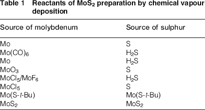
One of the most popular vapour deposition methods involves reacting Mo with S precursor gas evaporated from a solid sulphur source. This approach can facilitate large area synthesis of MoS2 films over a length scale of a few inches. Zhan et al. have directly prepared monolayer and few layered MoS2 on substrates by predepositing an Mo film in sulphur (113°C) using CVD. 8 Figure 1a shows the typical procedure: first, a thin layer of Mo was predeposited on SiO2/Si by e-beam evaporation, then S was introduced and reacted with Mo at 750°C for 10 min, using N2 as a protective atmosphere, which forms a very thin film of MoS2. The size and thickness of the MoS2 layer depend on the size of the substrate and the thickness of the predeposited Mo. Laskar et al. showed for the first time that CVD on epitaxial substrates can generate large area, oriented crystalline films of unprecedented high quality by sulphurising e-beam evaporated Mo films. 44 The growth temperature and choice of substrate critically impacted the quality of the grown film. They sulphurised samples at 500, 700, 900 and 1100°C for 12 h, and their results suggest that the films grown at higher growth temperatures had much higher structural quality than those grown at lower temperatures. Lee et al. developed a large area synthesis method for preparing high quality MoS2 films using H2S gas and a Mo metal source (Fig. 1b). 45 First, they deposited Mo metal on SiO2/Si or a quartz wafer by e-beam evaporation and then placed the samples in a tube furnace, which they heated to 750°C under rough vacuum. After preannealing the Mo, they injected a reaction mixture of H2S/H2/Ar to synthesise MoS2 over 15 min; during synthesis, the chamber pressure was 3·1 × 10− 1 torr.
Variety of preparation methods of MoS2 film. a model of introducing S to Mo thin film predeposited on SiO2 substrate, CVD system used to prepare MoS2 samples and SiO2/Si substrate with few layers of peeled MoS2. 8 b schematic of growth and transfer system used to prepare MoS2 films; CVD can be used to synthesise large area MoS2 films on SiO2/Si wafer or quartz substrate. This film can be transferred to arbitrary substrate. 45 c schematic of experimental set-up, and AFM image of monolayer MoS2 film on SiO2/Si substrate. 49 d schematic of promoter and growth substrates, showing various regions (A-P) divided according to distance from promoter substrate to growth substrate, along with corresponding optical images of MoS2 flakes in those regions. 52 e schematic of synthesising MoS2 layers by MoO3 sulphurisation. First, MoO3 layer is thermally evaporated on sapphire substrate, then MoO3 is converted to MoS2 by two-step thermal process. 54 f Growth set-up, conditions and SEM of triangular MoS2 monolayer 57
Another CVD method involved using MoO3 in place of the Mo metal source. Sulphurising MoO3 has been comprehensively studied; it is the main MoS2 synthesis technique, as MoO3 has low melting and evaporation temperatures.
46
Typically, MoO3 is partially reduced by sulphur vapour to form volatile MoO3-x species, which flow downstream in a carrier gas, adsorb onto the substrate, diffuse on the surface and react with sulphur to rearrange into MoS2 layers (equation (1))47,48

The growth conditions of MoS2 are very sensitive to surface treatment. Layer growth can be promoted with aromatic molecules, such as graphene, reduced graphene oxides, perylene-3,4,9,10-tetracarboxylic acid tetrapotassium salt and perylene-3,4,9,10-tetracarboxylic dianhydride, as well as with F16CuPc and CuPc.49,52,53 Lee et al. used various aromatic molecules as seeding promoters to produce large area, highly crystalline, uniform MoS2 monolayers with CVD (Fig. 1d). Growing MoS2 also depends on seed concentration. For example, Fig. 1d shows a promoter substrate covered with condensed perylene-3,4,9,10-tetracarboxylic acid tetrapotassium salt seeding promoters. The growth substrate was divided into various regions (A–P), which shows the different flake sizes and surface coverage varied in interesting ways. From region I onward, the size of monolayer flake decreases gradually, but the density of the flake appears to be increased.
Lin et al. deposited MoO3 on a c-face sapphire substrate using a thermal evaporator.
54
First, they placed an MoO3 film coated on a c-face sapphire substrate in the cold zone of a quartz tube flowing with Ar/H2. When the centre of the furnace reached 500°C, they moved the substrate to the hot zone for the first anneal. After 1 h, they moved the sample to the cold zone and placed a ceramic boat of S powder in the cold zone. After the hot zone reached 1000°C, they moved the samples and the boat to the centre of the furnace for a second anneal for 30 min with Ar flowing at 70 sccm (Fig. 1e). The chemical equations for the two-step reaction are proposed in equations (2) and (3)


Wu et al. reported a new, straightforward method for obtaining monolayer MoS2 with high optical quality, 57 using MoS2 powder as the source of both Mo and S. The powders were placed at the centre of a horizontal quartz tube furnace, maintaining the carrier gas flow and setting the pressure to ∼20 torr. The furnace temperature was increased to ∼900°C, holding it for 15–20 min (Fig. 1f ). In this way, MoS2 can be grown on various insulating substrates, which should facilitate device fabrication without need for a transfer process.
In the earlier time, Mo(CO)6 and H2S can be used to produce MoS2 in the temperature range of 175 to 300°C.58,59 After a short while, researchers found that the MoS2 films can be deposited by reaction of molybdenum halides with H2S. 60 Lee et al. reported that the MoS2 CVD film was fabricated by reaction of H2S with MoF6 at 1 kPa and at temperature as low as 703 K. 61 Endlera et al. obtained MoS2 lubricant coatings film using a gas mixture of MoCl5, H2S and Ar. 62 In 2014, Yu et al. synthesised MoS2 atomic films by placing MoCl5 and S powders in a furnace at a growth temperature of 850°C, flowrate of 50 sccm and pressure of ∼2 torr. 63 Cheon et al. deposited MoS2 from the metal organic precursor Mo(S-t-Bu)4. 64 The MoS2 film was deposited using a Pyrex high vacuum apparatus containing substrate temperatures of 110–350°C and a pressure of 10− 4 torr, and the film thickness depended on the deposition time and the total precursor flux. However, in recent years, few have used MoCl5 and Mo(S-t-Bu)4 as Mo sources.
There are many types of CVD, including low pressure CVD, which is the most common type. 65 In this method, the reaction chamber in the furnace should be at low pressure; this makes the reaction more downy, which is better than depositing on a single sample. Other methods include metal organic CVD and plasma activated CVD,66–68 which can produce films and nanoparticles. However, these methods are not usually used to produce MoS2 films.
Physical vapour deposition (PVD)
An early application of MoS2 was lubrication, as surface coating can effectively improve the durability of materials used in aggressive environments.69,70 Methods useful for depositing coatings include PVD and magnetron sputtering.33,71
Recently, some researchers have tried to prepare MoS2 films by PVD. 72 Most recent papers have reported monolayer MoS2 exhibiting triangular morphology. However, the triangular morphology appeared as early as 2000 in samples produced by PVD. 73 Later, Lauritsen et al. obtained the same morphology of triangular MoS2. Initially, they deposited Mo by PVD onto Au(111) in H2S at 10− 6 mbar at 400 K. The Au substrate acted as a nanotemplate. They then annealed the substrate at 673 K for 15 min in H2S. The cluster morphology of the triangular MoS2 that they produced depended strongly on the size of substrate. 74
Depositing metal contacts may also substantially affect the structure and electronic properties of MoS2.75,76 For example, Gong et al. deposited three different metals (Pd, Au and Ag) on monolayer MoS2. 77 They placed MoS2 powder source downstream, far from the oven centre in a cooler zone, and increased the furnace temperature to 900°C, keeping the growth temperature to ∼650°C. For experimental details, refer to Ref. 54. They heated the metals before deposition for 5 min, and then e-beam evaporated the metals on the MoS2 samples at 2 × 10− 6 torr. Their Raman spectra showed that Pd wet the MoS2, forming a uniform, intimate contact, while the Au and Ag adsorbed inhomogeneously.
Compositing, decorating and doping
MoS2 has received much attention because of its excellent properties. Researchers expect to improve the properties of MoS2 through compositing, decorating and doping. Many reports have investigated compositing and decorating MoS2 with graphene, metal oxides and noble metals.78–80 In this review, we discuss research on compositing, decorating and doping related to CVD.
Composite
Currently, graphene is one of the most studied compounding materials for MoS2.81,82 Yu et al. produced high performance graphene/MoS2 heterostructure device, using the MoS2 as the transistor channel and graphene as the contact electrodes and circuit interconnects (Fig. 2a). 83 They deposited 20 nm aluminium oxide (Al2O3) on the CVD-MoS2 by atomic layer deposition. Large area single layer graphene was then grown on Cu foils at 1035°C by CVD and transferred onto a sample in a vacuum probe station at 3 × 10− 6 torr. The result shows that this contact between graphene and MoS2 was ohmic, and the paper is the first demonstration of logic circuits using CVD grown 2D heterostructures. The output characteristics of their inverter, a low voltage of − 4 V represents logic state 0 and a voltage close to 0 V represents logic state 1.
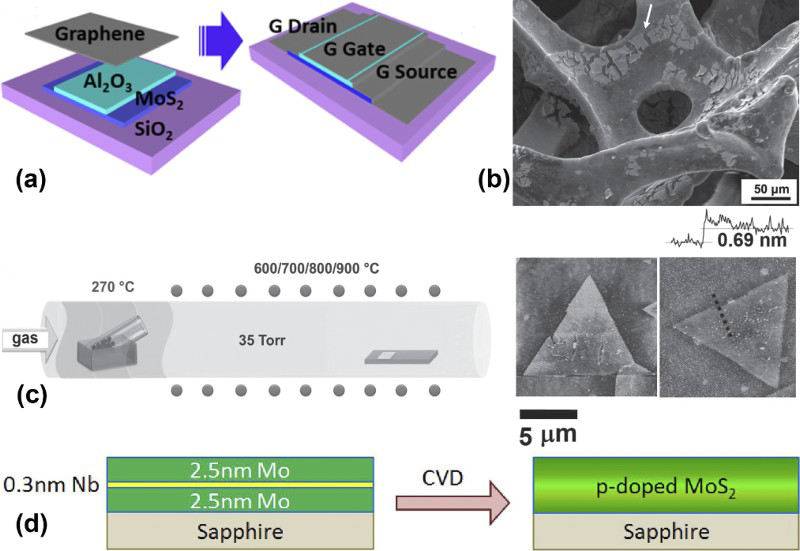
Compositing, decorating and doping of MoS2 film: a schematic of important steps to fabricate large scale electronics from graphene/MoS2 heterostructures, using MoS2 as channel and graphene as contact electrodes and interconnects; 83 b SEM image of MoS2/3DGN composite (arrow indicates microscale MoS2 flakes); 84 c selenised MoS2 (at 800°C) on sapphire substrates; 88 d schematic of Nb doping in CVD grown MoS2 94
As a different example of composite films, Zhang et al. produced MoS2 coated 3D graphene networks (3DGNs) (Fig. 2b). 84 After synthesising the 3DGNs by CVD, they prepared an MoS2 precursor solution by mixing (NH4)2MoS4 in dimethylformamide. Then, they placed the 3DGNs into the MoS2 precursor solution for 5 min, before transferring it to the CVD chamber. The CVD chamber was pumped down to 10 mtorr, and the MoS2 precursor coated 3DGNs were annealed at 50°C for 1 h. Then, the temperature was increased to 400°C in an Ar/H2 protective atmosphere. After the temperature stabilised, the MoS2 precursor coated 3DGNs was annealed at 400°C for 1 h. Then, the furnace was cooled naturally to room temperature. The MoS2/3DGN composite exhibited good cycling performance when used as an anode for lithium ion batteries. It exhibited reversible capacities of 877 and 665 mA h g− 1 during the fiftieth cycle at current densities of 100 and 500 mA g− 1 respectively.
Decorating
To improve the performance of hydrodesulphurisation in petroleum, researchers have attempted to deposit Co on MoS2.85,86 For example, Okamoto deposited Co(CO)3NO onto MoS2 catalysts supported on SiO2. They presulphided MoS2/SiO2 in a 10%H2S/H2 stream at 400°C using Co(CO)3NO. 87 After exposing the MoS2/SiO2 to the Co(CO)3NO vapour for 5 min, they evacuated the sample for 10 min at room temperature, and then performed a second sulphidation under the same conditions as the first.
MoS2 is very interesting because its band gap changes from indirect in the bulk crystal to direct in single layers. Li et al. reported that the CVD grown MoS2 monolayer flakes can be selenised in the presence of selenium vapour on sapphire substrates. 88 First, they placed as grown triangular monolayer MoS2 at the centre of a quartz tube furnace. Then, they heated Se powder, placed close to the open end of the furnace at the upstream position, to 270°C and various other temperatures using a separate heating belt for 4 h. As the selenisation temperature changed, the band gap varied from 1·86 to 1·57 eV (Fig. 2c).
Shi et al. decorated the edges of monolayer MoS2 with Au nanoparticles using a controllable wet method. 89 Using MoO3 and S as precursors for CVD, they produced high quality crystalline MoS2, which they directly immersed in 5 mM AuCl3 for 20 s. They formed MoS2 transistors with an ionic gel film, which works as a dielectric layer. Decorating the MoS2 with Au NPs decoration changed the threshold gate voltage from 0·47 to 1·29 V and shifted the Fermi level in MoS2 layers down. Decorating the device increased the on/off ratio by ∼50 times.
Doping
Dopants are impurities that enhance electrical conductivity and photocurrent gain. 90 Currently, research on doped MoS2 is very limited. Rhenium doped MoS2 single crystals have been grown using chemical vapour transport with Br2 as the transport agent. 91 In this study, pure Mo, Re and S were sealed in a quartz ampoule containing Br2; at a temperature gradient of approximately 960–930°C, the productions are MoS2 doped with 0·5–1% rhenium.
Doped niobium was reported several decades ago,92,93 but only large crystals were investigated. In 2014, Laskar et al. reported a CVD method for niobium doped MoS2. 94 Using e-beam evaporation, they produced Mo (2·5 nm)/Nb/Mo (2·5 nm) on sapphire, which they sulphurised in a CVD chamber at 900°C for 10 min (Fig. 2d ). They found that Nb can act as an efficient acceptor in MoS2 leading to a high hole density and relatively high mobility: at room temperature, a hole concentration of 4 × 1020 cm− 3 and hole mobility of 8·5 cm2 V− 1 s− 1.
Applications of MoS2
Graphene is the most widely studied 2D material because of its high carrier mobility and electrical conductivity.95,96 However, graphene has no band gap, and it is very complex to design graphene with band gap. Meanwhile, the mobility will be reduced due to the design. MoS2 is a current research focus across a broad range of disciplines.
MoS2 is a current research focus across a broad range of disciplines. MoS2 has unique features as a channel material in field effect transistor.97,98 Wang et al. fabricated top gated transistors on single layer MoS2 grown by CVD for the first time. 99 They obtained MoS2 using MoO3 and S powder; then, a 5 nm Ti/50 nm Au metal stack was deposited on the MoS2 film. Then, the top gate dielectric consisting of 30 nm HfO2 was deposited. Lastly, the top gate was formed by depositing 50 nm Pd. The maximum on-state current of their device reached 16 μA μm− 1, and its threshold voltage was − 2 V. The extracted carrier mobility of this polycrystalline CVD single layer MoS2 was above 40 cm2 V− 1 s− 1.
The unique structure of layered MoS2 forms a smooth surface. The free dangling chemical bonds on the surface makes it suitable for highly efficient Schottky barrier solar cells. Shanmugam et al. deposited MoS2 nanomembranes using Mo and S powder in the Ar environment. 100 With a simple stacked structure of indium tin oxide/MoS2/Au, their fabricated solar cell exhibited a photoconversion efficiency of 0·7% for 110 nm MoS2 and 1·8% for 220 nm MoS2.
The band gap of MoS2 is tuneable, which may allow for engineering of optical absorbance in photovoltaics. MoS2 phototransistor has been extensively studied because of the photosensitive of thin films MoS2.30,101 Zhang et al. constructed a phototransistor based on a graphene/MoS2 hybrid device by CVD. 102 The measured responsivity of the graphene/MoS2 transistor was up to ∼1 × 10⁴ mA W− 1 with an incident power of 0·645 μW at VDS = 0·1 V and VBG = 0 V. This responsivity was higher than that of a MoS2 phototransistor and graphene phototransistor at the same conditions.
In addition, MoS2 also has many promising applications, including lubricant, lithium storage, biosensors, gas detectors and integrated circuits12,103–106 because MoS2 has a large band gap of 1·2–1·9 eV, high mobility, excellent current on/off ratios and high natural abundance. 20
Outlook and future challenges
Two-dimensional graphene-like molybdenum disulphide is a relatively new and exciting material that has many unique properties, making it promising for a number of applications. MoS2 films, especially monolayer films, are necessary for most transistor applications, including field effect transistors, phototransistors, integrated logic circuits and gas and biological sensors. It will likely be the material of choice for ultra thin, transparent, flexible conductors in transparent, flexible devices.
Research in MoS2 films has increased gradually, but there are many unknowns to explore. Currently, challenges in preparing MoS2 by CVD include uniformity, controllable size, thickness and high quality. To improve the performance and application of MoS2 films, we must find experimental conditions that can better produce these materials more efficiently and more safely. To increase the performance of MoS2 devices, we must explore creating heterostructures by integrating layered MoS2 with other layered materials. Achieving large area, uniform, high quality MoS2 films still requires much effort, specifically involving the development of new fabrication processes to control the thickness and transport properties of the MoS2, an exciting and rapidly expanding area of research.
Footnotes
Acknowledgement
This work is supported by the National Natural Science Foundation of China (grant nos. 61076039, 61204065, 61205193, 61307045, 61404009 and 61474010), Research Fund for the Doctoral Program of Higher Education of China (grant no. 20112216120005), the Developing Project of Science and Technology of Jilin Province (grant nos. 20121816, 201201116, 20140520107JH and 20140204025GX), National Key Laboratory of High Power Semiconductor Lasers Foundation (grant no. 9140C310101120C031115).