
Abstract
Al doped CdZnTe film was prepared by radio frequency magnetron sputtering with aluminium induced crystallisation. Structural and electric properties of Al doped CdZnTe film were studied. Al doped CdZnTe film has a preferred [111] orientation with uniform pebble-like grain structure, and the leakage current is 2·3 × 10− 8 A. Current conduction mechanism in Al doped CdZnTe film has been investigated and analysed. Space charge limited current emission is found to be the dominant mechanism in Al doped CdZnTe film, which was associated with trapping process of Cd vacancies.
Introduction
Special attention has been given to CdZnTe films for optoelectronic devices such as X-ray and gamma-ray detectors because of its low leakage currents and high quantum efficiency in detectors at room temperature.1,2 The doping CdZnTe films are very useful in devices because they produce considerable changes in their structural and physical properties.3,4 The doping CdZnTe films can be prepared by various methods, including thermal evaporation, radio frequency (rf) magnetron sputtering, electrodeposition and closed space sublimation.5–8 However, these methods suffered the problem of defects and non-uniform composition during the deposition process, thus causing descend of resistivity and homogeneity in CdZnTe film, which limits its application. From this reason, rf magnetron sputtering with aluminium induced crystallisation (AIC) method was proposal to fabricate high resistivity Al doped CdZnTe films.
The Al doped CdZnTe film prepared by AIC technology based on the deposition of CdZnTe precursor layer capped with a thin aluminium film formed recrystallisation CdZnTe film by thermal annealing. 9 The Al doped CdZnTe film by AIC has advantages of simple instrumentation, perfect crystallinity and excellent electrical properties. In this work, structural, surface composition and electrical conduction of Al doped CdZnTe film by AIC were studied.
Experimental
The Al doped CdZnTe film was deposited on ITO glass substrates by rf magnetron sputtering with AIC technology. CdZnTe and Al layers were deposited by rf and direct current (dc) magnetron sputtering respectively. Cd0·9Zn0·1Te crystal target with 60 mm diameter and high purity aluminium (purity 99·999%) were used. The distance of substrate target was 5 cm. The base pressure before sputtering was 8·0 × 10− 4 Pa. The work pressure was 1·5 Pa. CdZnTe layer was first deposited on substrate with rf sputtering power of 80 W for 1 h. Subsequently, an Al layer was deposited on the CdZnTe layer by dc magnetron power of 100 W for 10 min. To perform the AIC of CdZnTe/Al layered structure, the samples were heated at 200°C for 1 h. Finally, dilute sodium hydroxide solution was used to remove the residual aluminium layer on the CdZnTe surface.
Without the AIC technology, undoped CdZnTe film (thickness, 1 μm) deposited at the same preparation conditions was a reference sample.
The structure of the CdZnTe films was tested by X-ray diffraction (XRD). The surface morphology of the CdZnTe films was observed by atomic force microscopy (AFM). The X-ray photoelectron spectroscopy (XPS) was used to determine the surface composition of CdZnTe films. I–V curve of CdZnTe films was measured using Keithley 4200-SCS source meter. Ag top electrodes with an effective area of 10− 2 cm2 were sputter deposited with a shadow mask.
Results and discussion
Typical XRD patterns obtained for the undoped and Al doped CdZnTe films are shown in Fig. 1. The diffraction peak observed at 2θ = 23·8° has been identified as the (111) diffraction peaks of CdZnTe, which suggests that the CdZnTe film is single phase formation with a preferred [111] orientation.
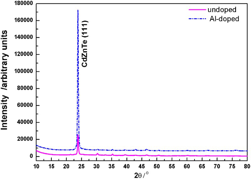
XRD graphs of undoped and Al doped CdZnTe films
The surface morphology of film was investigated by AFM, as shown in Fig. 2. The mean grain diameter of undoped CdZnTe film is ∼50 nm. Al doped CdZnTe film shows pebble-like crystal grains with a mean diameter of 140 nm. The grain of Al doped CdZnTe film becomes more uniform and larger than that of undoped film. The reason for the change in morphology may be due to the heterogeneous nucleation of aluminium in the CdZnTe layer. 10
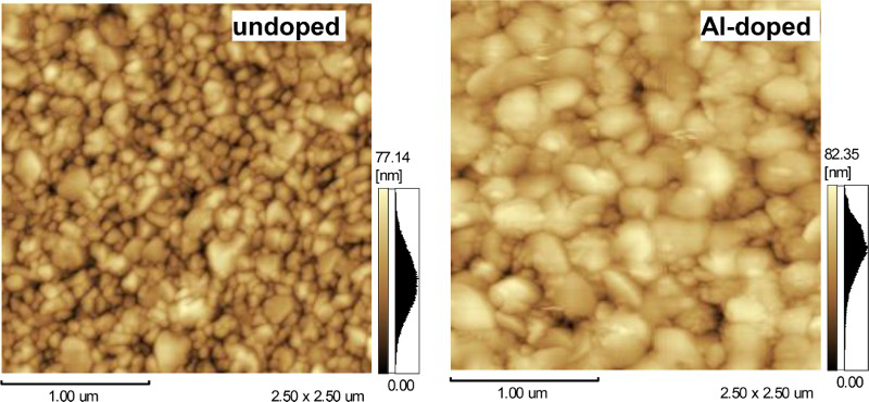
AFM micrograph of undoped and Al doped CdZnTe films
The surface composition of CdZnTe films has been studied by XPS. Figure 3 shows the XPS spectra of the CdZnTe films. The binding energy regions of Cd3d, Zn2p and Te3d were obtained. The binding energies of Cd(3d5/2 and 3d3/2), Zn(2p1/2 and 2p3/2) and Te(3d5/2 and 3d3/2) levels were 405·1 and 411·9 eV, 1045 and 1021 eV, and 572·5 and 582·9 eV respectively. It is apparent that Te–O bonding is present at the film surfaces as indicated by the peaks at 576·2 and 586·5 eV along with the expected Te peaks. It was indicated that TeO2 and CdTeO3 were formed in the surface of the films.11–13 The composition of undoped CdZnTe film is 51·27 at-% Te, 45·16 at-% Cd and 3·57 at-% Zn. The composition of Al doped CdZnTe film is 50·21 at-% Te, 43·76 at-% Cd, 4·6 at-% Zn and 1·43 at-% Al. It is worth noting that the surface of the undoped and Al doped CdZnTe films is rich in Te atoms. The values of Zn concentration (x = [Zn]/([Zn]+[Cd])) of undoped and Al doped films are 0·07 (Cd0·93Zn0·07Te) and 0·1 (Cd0·9Zn0·1Te) respectively. The composition of Al doped CdZnTe film agreed with the Cd0·9Zn0·1Te target.
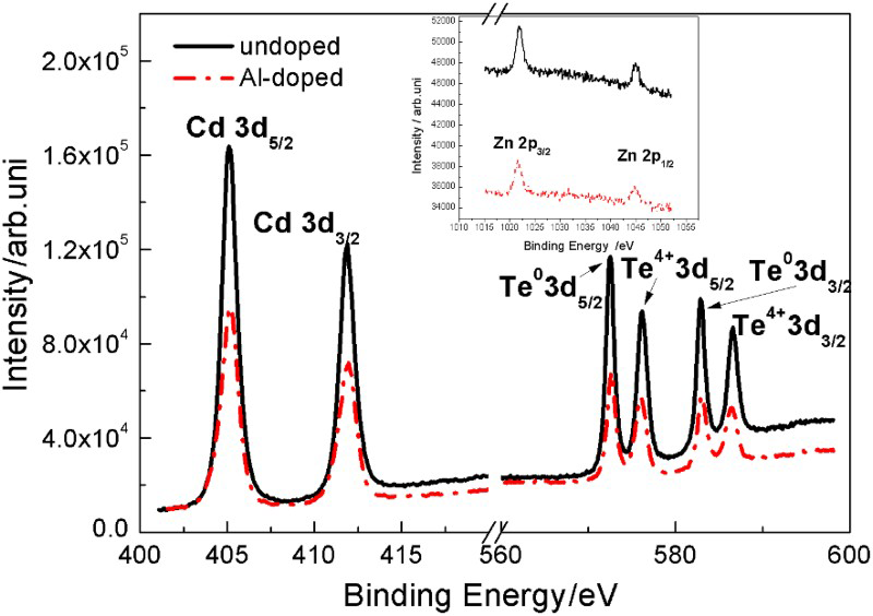
XPS spectra of undoped and Al doped CdZnTe films
Typical I–V characteristics of the undoped and Al doped CdZnTe films were shown in Fig. 4. The leakage current in undoped CdZnTe film was 3·3 × 10− 6A at a bias voltage of 2 V. However, for Al doped CdZnTe film, the leakage current was 2·3 × 10− 8 A, which satisfies the noise requirement of nuclear detectors. The resistivity of undoped and Al doped CdZnTe films is approximately equal to 5·6 × 107 and 8·5 × 109 Ω cm respectively.
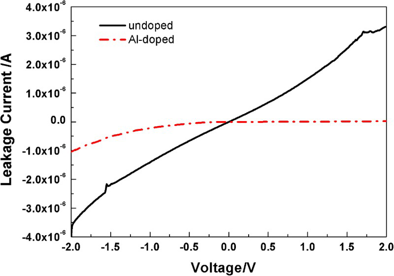
I –V curves of undoped and Al doped CdZnTe films
To understand the improvement of resistivity, study of current conduction mechanisms of undoped and Al doped CdZnTe films is very essential. The relationship between electric field (E) and leakage current density (J) of the undoped and Al doped CdZnTe films is shown in Fig. 5. J–E curve of undoped CdZnTe film is linear, and the conduction mechanism is ohmic conduction, which is related to the charge transfer process between ionic and electronic conductors.
15
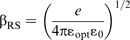
J–E curve of Al doped CdZnTe film exhibits a polynomial relation, implying the existence of space charge limited current (SCLC), Schottky and Poole–Frenkel (PF) conduction mechanisms.16–18 We have plotted the relationships of J–E2, ln J–E1/2 and ln(J/E)–E1/2 in Fig. 6 along with the measured J–E data of Al doped CdZnTe film. For the equations of PF effect and Schottky emission, there is a constant of
 , which shows the conduction mechanism. The constant of Schottky emission
 and the constant of PF effect
 can be calculated by the following equations
19
:
can be calculated by the following equations
19
:

 F m− 1, the dielectric permittivity of vacuum
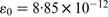 F m− 1 and
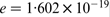 C. The theoretical values of
 and
and
 are 1·4 × 10− 5 and 2·8 × 10− 5 eV respectively. At 300 K, the theoretical slopes of Schottky and PF emission, corresponding to
 , were 5·4 × 10− 4 and 1·1 × 10− 3 respectively. However, the measured slopes of ln J–E1/2 and ln (J/E) − E1/2 are 4·4 × 10− 2 and 1·6 × 10− 2 respectively. The experimental slope is largely different to the theoretical slope. This suggests that neither Schottky nor PF mechanism is the dominant conduction. A linear J1/2 − E relation is shown in Fig. 6, which corresponds to the SCLC conduction. According to the SCLC theory, we established a ‘triangle’ in a log (J)–log (E) plot. Ohm's law and Child's law obey20–22

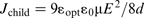
 ,
,
 and d are electronic charge, carrier concentration, and carrier mobility and thickness of the sample respectively. With the fitting of J–E curve of Al doped CdZnTe film with the Ohm's law and Child's law, the slopes of Ohm's law and Child's law are 1·78 × 10− 11 and 3·2 × 10− 11 respectively. The calculated carrier concentration and mobility in Al doped CdZnTe films are 2·4 × 108/cm3 and 0·45 cm2 (V s)− 1 respectively. Compared with hole mobility of 27 cm2 (V s)− 1 reported by literature,
23
mobility of Al doped CdZnTe films is reduced.
and d are electronic charge, carrier concentration, and carrier mobility and thickness of the sample respectively. With the fitting of J–E curve of Al doped CdZnTe film with the Ohm's law and Child's law, the slopes of Ohm's law and Child's law are 1·78 × 10− 11 and 3·2 × 10− 11 respectively. The calculated carrier concentration and mobility in Al doped CdZnTe films are 2·4 × 108/cm3 and 0·45 cm2 (V s)− 1 respectively. Compared with hole mobility of 27 cm2 (V s)− 1 reported by literature,
23
mobility of Al doped CdZnTe films is reduced.
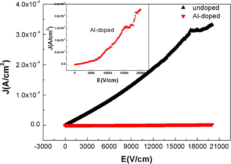
Electric field dependence of leakage current density of undoped and Al doped CdZnTe films
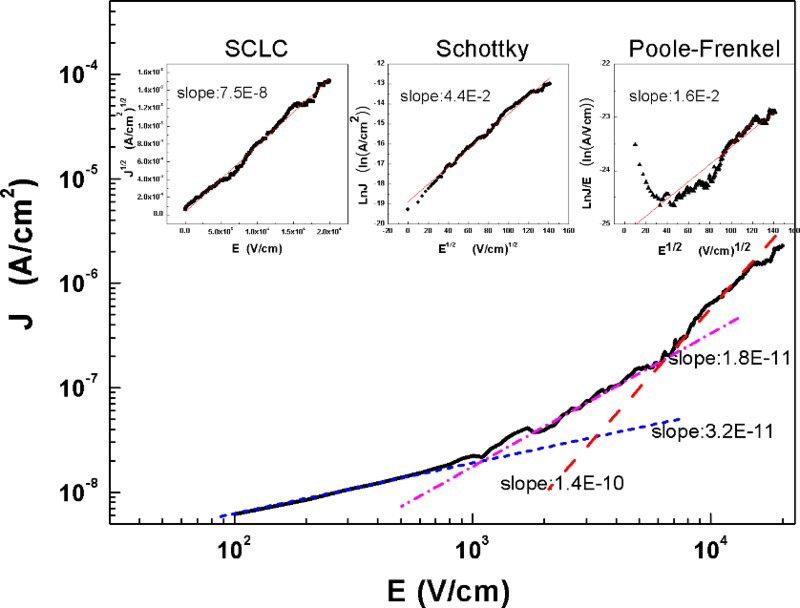
J –E curve of Al doped CdZnTe films; insets show plots of J –E2, lnJ –E1/2 and In(J/E) − E1/2 for the SCLC, Schottky and PF conduction mechanisms respectively
In our opinion, SCLC in Al doped CdZnTe films is bulk limited conduction, which was associated with the trapping process of the free carriers. In Al doped CdZnTe film, Al atom acted as a donor occupying Cd vacancy. The acceptor of Al doped CdZnTe film is complex defect (VCd–AlCd) or (VCd–2AlCd). 24 The shallow traps and deep donors are coexistence in CdZnTe films. The deep donors compensate Cd vacancy, which was associated with the free carriers trapped by the Cd vacancies.
Conclusions
Al doped CdZnTe film was prepared with the AIC technology, which has a finer and more uniform pebble-like structure due to the heterogeneous nucleation of aluminium in CdZnTe layer.
The surface composition of the Al doped and undoped CdZnTe films has slightly Te rich state, and the composition of Al doped CdZnTe film agreed with the Cd0·9Zn0·1Te target.
The resistivity of Al doped CdZnTe film is 8·5 × 109 Ω cm. The conduction mechanism of Al doped CdZnTe films is space charge limited. The calculated carrier concentration and mobility in Al doped CdZnTe films are 2·4 × 108/cm3 and 0·45 cm2 (V s)− 1 respectively.
Footnotes
Acknowledgements
This work was supported by the National Natural Science Foundation of China (grant no. 51002012) and Beijing Institute of Petrochemical Technology Breeding Project of Outstanding Young Teachers and Management Backbones (grant no. BIPT-BPOYTMB-2014).