
Abstract
The effects of Ni content on the structural, optical, dielectric and electrical properties of Bi1·5Zn0·92Nb1·5O6·92 pyrochlore ceramics have been investigated. Nickel atoms were inserted into pure samples in accordance to the composition Bi1·5Zn0·92Nb1·5−xNixO6·92−3x/2, with x varying from 0·07 to 0·40. The structural analysis revealed that a single phase of the pyrochlore compound can be obtained for x values of 0·07 and 0·10 only. Further increase in Ni caused the appearance of multiple phases. The optical energy band gaps are determined as 3·30, 3·35 and 3·52 eV for Ni content of 0·00, 0·07 and 0·10 respectively. The temperature dependent electrical resistivity and the frequency dependent capacitance are observed to increase with increasing Ni content. The resonance frequency, which was determined from the capacitance–frequency dependence, was observed to shift from 12·14 to 10·47 kHz as the x values increase from 0·00 to 0·10 respectively.
Introduction
Deficient pyrochlore oxides have attracted great interest due to their potential applications in various technological areas such as ionic conductors,1 oxygen electrodes2, 3 and solid electrolytes in rechargeable batteries.4 Deficient pyrochlore of the form AB2X6 is reported to exhibit superconductivity5 and unusual magnetic properties as well.6–8 Extensive research has been performed on the structural, physical, electrical and dielectric properties of pyrochlores. Ideal pyrochlore structures have a general formula of A2B2X6Z, where A and B are cations, and X and Z are anions. By removing A and/or B cations or Z anion from the ideal pyrochlore structure, a variety of deficient pyrochlores can be obtained.
Bismuth based pyrochlores related to the Bi2O3–ZnO–Nb2O5 ternary system are promising materials for high frequency filter applications due to their temperature stability, low loss and high permittivity.9–12 Moreover, their low firing and sintering temperatures (850–950°C) and compatibility with Ag allow them to be co-fired with Ag for the purpose of preparation of multilayer devices.13, 14 Bi2O3–ZnO–Nb2O5 based ceramics were explored in the 1970s as temperature stable and temperature compensating multilayer ceramic capacitors.15 Levin et al.16 studied the Bi1·5Zn0·92Nb1·5O6·92 phase using X-ray diffraction (XRD) and neutron powder diffraction techniques, and they concluded that the cubic pyrochlore had a lattice parameter of 10·5616±0·0001 Å with both Bi and Zn mixed on the A sites or Zn cations present on both A and B sites. The dielectric properties of Bi1·5Zn0·92Nb1·5O6·92 pyrochlore have also been well investigated.10,17–20 Bi1·5Zn0·92Nb1·5O6·92 has a high dielectric constant k and a high Q×f value at 2·3 GHz (k≈126 and Q×f = 550 respectively).21
Although numerous articles that discuss the preparation conditions and the structural and compositional and dielectric properties of Bi1·5Zn0·92Nb1·5O6·92 pyrochlore ceramics are available in the literature, little optical and electrical data on the bulk form have been reported. The main purpose of this work is to study and discuss the effect of nickel doping on the structural, optical and electrical properties of Bi1·5Zn0·92Nb1·5O6·92 pyrochlore ceramics.
Experimental
Ceramic samples were prepared by the conventional solid state reaction. Raw materials of Bi2O3, (99·99%, Aldrich), Nb2O5 (99·5%, Merck), ZnO (99·5%, Aldrich) and NiO were weighed according to the composition Bi1·5Zn0·92Nb1·5−xNixO6·92−3x/2, where x = 0·07–0·40. The weighed oxides were wet mixed and milled in ethanol for 4 h in a polyethylene bottle using zirconia milling media and calcined at 800°C for 4 h in a closed alumina crucible. The ground calcined powders were uniaxially pressed into a disc (∼10 mm in diameter and 0·5–1·5 mm in thickness d), which was then sintered at 1000°C for 4 h in a tightly closed alumina crucible in air. The sintered disc density was measured using Archimedes’ water immersion technique. The Ni doped single phase Bi1·5Zn0·92Nb1·5O6·92 ceramics sintered at 1000°C for 4 h had relative densities over 97%. The crystalline phase of the sintered samples was identified by XRD technique (Rigaku model, 1° min−1, 2θ = 10–70°) with nickel filtered Cu Kα radiation. Lattice parameters were refined by the least square refinement procedure. This is a process of improving the parameters of an approximate (trial) structure until the best fit is achieved between an observed diffraction pattern and that calculated by Fourier transformation from the numerically parameterised trial structure. It is performed by least-squares minimisation between the experimental structure factors and those calculated by varying the adjustable parameters of the structural model.
The optical data of the samples were recorded using a Perkin-Elmer Lambda EZ 201 spectrophotometer. The electrical contacts were made using silver paste. The electrical data were recorded using a Phywe high voltage (0·0–2·0 MHz) wave function source, a Mastech RC meter and a Keithley 485 picoammeter.
Results and discussion
The XRD pattern of the Bi1·5Zn0·92Nb1·5O6·92 pyrochlore ceramic (BZN), which is illustrated in Fig. 1, was analysed using the Crystallographica software. The collected data indicated the single phase appearance of the pyrochlore. No additional phases were observed. Since the XRD data of Bi1·5Zn0·92Nb1·5O6·92 pyrochlore did not show any superlattice reflections, it is assumed that the Bi and Zn cations are randomly distributed over the A site, while the Nb and Zn cations are distributed over the B site in the A2B2O7 pyrochlore.22, 23 The Miller indices (hkl) are also displayed in Fig. 1. The lattice parameters of the cubic unit cell, evaluated by the least squares method for the BZN pyrochlore sintered at 1000°C for 4 h, were found to be 10·5616±0·0004 Å. This value is close to that we have previously reported as 10·442 Å for the Bi1·5ZnSb1·5O7 pyrochlore sintered at 1200°C for 5 h.24 Careful analysis of the Miller indices (Fig. 1) has revealed that nearly for all the obtained intensive X-ray patterns, the total sum of the indices (h+k+l) is even, and all the odd reflection sums of the (h+k+l) are weak. This behaviour indicates that the Bi1·5Zn0·92Nb1·5O6·92 pyrochlore ceramic may have a face centred cubic structure.
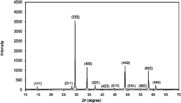
X-ray diffraction pattern of Bi1·5Zn0·92Nb1·5O6·92 pyrochlore
Since the ionic radius of the Ni element (0·69 Å) is near the ionic radius of Nb (0·64 Å), Ni was doped into the Nb site of the BZN pyrochlore. For this purpose, the composition of Bi1·5Zn0·92Nb1·5−xNixO6·92−3x/2, with x being varied from 0·07 to 0·4, was used. The XRD patterns for the Ni doped samples are displayed in Fig. 2. Analysis of the Ni doped X-ray patterns has shown that a single phase pyrochlore compound can be obtained only when x is 0·07 and 0·10. When x is 0·15, ZnO second phase [Joint Committee on Powder Diffraction Standards (JCPDS) card no. 13-0311] started to form (Fig. 2). At higher Ni doping values, phases other than ZnO appeared. At x = 0·30, a high amount of Bi5Nb3O15 phase (JCPDS card no. 16-293) and a low amount of Bi2O3 phase (JCPDS card no. 18-244) were detected. The amounts of Bi5Nb3O15 and Bi2O3 increase with increasing Ni. The lattice parameters of the Ni doped BZN pyrochlore ceramics, Bi1·5Zn0·92Nb1·43Ni0·07O6·815 and Bi1·5Zn0·92Nb1·4Ni0·1O6·77, sintered at 1000°C for 4 h were determined by the least squares method and found as 10·5429±0·0004 and 10·5486±0·0004 Å respectively. The lattice constant data for undoped and Ni doped samples suggest that the doping has reduced the lattice constant of the undoped one from 10·5616 to 10·5429 Å. Furthermore, increasing the content of Ni increases the values of the lattice parameters. The attenuation of the lattice parameters with Ni content may be attributed to the ionic radius of Ni being larger than that of Nb. However, it should always be noticed that the XRD determines only the average periodic structure and does not offer insights to any local structural distortion.
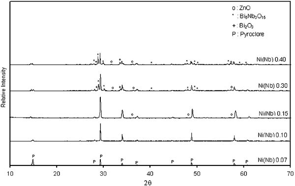
X-ray diffraction patterns of Bi1·5Zn0·92Nb1·5−xNixO6·92−3x/2 ceramics for different Ni doping values
The optical absorption coefficient α of the undoped and Ni doped with 0·07 and 0·10 samples was calculated from the measured transmittance T, displayed in the inset of Fig. 3, and reflectance R was computed using the relation T = (1−R)2 exp (−ad) in the incident photon energy region of 3·1–5·8 eV at 300 K. The data are displayed in Fig. 3. For the pure sample, the absorption coefficient sharply falls from ∼12 cm−1 at 5·8 eV to 5·6 cm−1 at 4·8 eV; thereafter, it decreases very slowly and tends to remain constant. In other words, the absorption coefficient does not reach a zero value; even at low incident photon energy, below the absorption edge, the α value is ∼5·6. This behaviour of the absorption coefficient was also observed for Tl2InGaSe4 crystal25, 26 and was attributed to the strength of the absorption at the ground state exciton energy. The same behaviour was observed for the doped samples. As can be seen from Fig. 3, Ni doping slightly decreases the value of the absorption coefficient, but it shifts the absorption edge significantly.
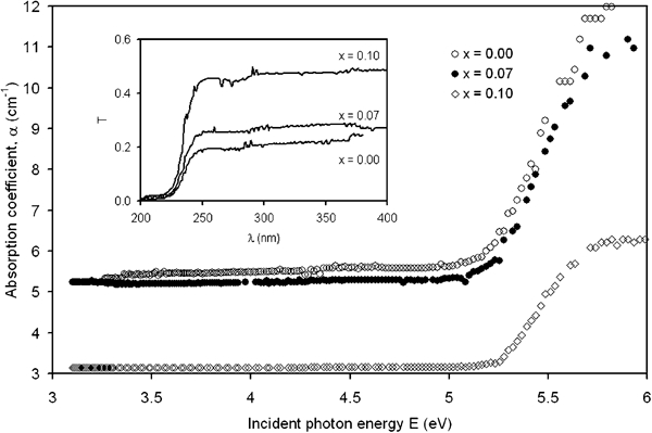
Optical absorption spectra for Bi1·5Zn0·92Nb1·5−xNixO6·92−3x/2 pyrochlore: inset represents transmission spectra
In the strong absorption region (5·8–4·8 eV), the absorption coefficient can be represented by the relation27

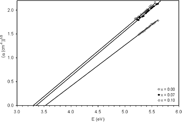
Plots of α1/3 as function of incident photon energy E for Bi1·5Zn0·92Nb1·5−xNixO6·92−3x/2 ceramics
The increase in the energy band gap from 3·30 to 3·35 and to 3·52 eV by increasing the nickel doping percentage suggests a widening of the energy band gap by Ni doping. The widening of the band gap with doping is a well known physical phenomenon and is observed for several composites like Ni doped Cu2O films deposited by reactive magnetron sputtering. The increase in N doping concentration up to 3% enlarged the energy band gap from ∼2·1 to ∼2·5 eV.30 This was attributed to the significant structural changes induced by N doping. Furthermore, by referring to our X-ray data analysis and recalling that the increase in nickel doping caused the appearance of multiple phases, the widening of the energy gap for the currently studied pyrochlore may be attributed to the structural modifications that come to stage by doping.
Figure 5 displays the electrical resistivity ρ for the undoped and Ni doped samples. The room temperature electrical resistivities were found to be 2·09×107, 6·04×107 and 6·94×107 Ω cm respectively. At all the applied temperatures,
 . Increasing the Ni content increased the electrical resistivity of the samples. This behaviour is mainly attributed to the band gap shrinkage, which was determined in this work by increasing the Ni content. The increase in electrical resistivity with increasing Ni content may also be due to the increased lattice imperfections. As reported through structural analysis, the increase in Ni content increases the values of the lattice parameter (due to the difference in ionic radios of Ni and Nb). It causes the appearance of other phases. The existence of more than one structural phase in a material increases the lattice mismatch and leads to many atomic vacancies that in turn increase the crystal imperfections.
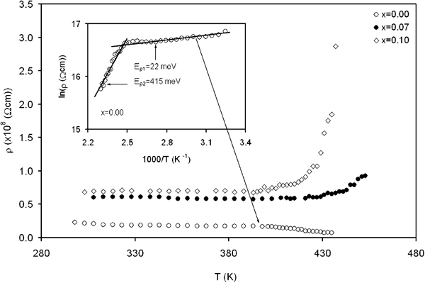
Variation of electrical resistivity with temperature for Bi1·5Zn0·92Nb1·5−xNixO6·92−3x/2 solid solution: inset reflects ρ−T−1 for pure sample
As may be seen from Fig. 5, the temperature dependence of the pure sample appears to be very different from that of the Ni doped ones. Particularly, while the resistivity of the pure sample decreases with increasing temperature in all the studied temperature range, the doped sample's resistivities are temperature invariant in the temperature range of 300–410 K. For temperatures >410 K, the resistivity of the doped samples increased with increased temperature. The constant electrical resistivity with increasing temperature may indicate that the electrical resistivity is not dominated by the bulk ceramic material but by the resistance of the ceramic surface contacts in the material. This behaviour could have happed due to the increased lattice imperfections.
The ln (ρ)−T−1 of the pure sample is displayed in the inset of Fig. 4. This sample reflects a typical semiconductor resistivity behaviour that can be represented by the relation ρ∝exp (Eρ/kT), with Eρ being the resistivity activation energy. The values of Eρ are 22 and 415 meV below and above 395 K as determined from the slopes of ln (ρ)−T−1, shown by solid lines, in the inset of Fig. 4. These values indicate the extrinsic nature of conduction due to thermal excitation of charged carriers. In contrast to the behaviour of pure samples, the doped samples did not show any thermal activation with temperature, and it reflects a trend of
 below and above ∼410 K respectively. The increase in electrical resistivity with increasing temperature could be explained by means of lattice vibrations. The higher the temperature, the wider the thermal vibration of atoms in the lattice, the less regular the atomic spacing (imperfection increased by doping), thus the less mobility of electrons in the ceramics.31
Figure 6 represents the capacitance dependence on the frequency f of the applied ac voltage Vac for the BZN ceramics being recorded at 300 K. It is clear from the inset that the capacitance initially raises sharply with increasing frequency up to critical values of 0·55, 0·68 and 0·710 nF at frequencies of 12·14, 10·70 and 10·74 kHz for the pure, 0·07 and 0·10 doped samples respectively. For higher applied frequency values, the capacitance falls sharply. The variation of the capacitance with frequency is mainly due to the dielectric constant of the material that reflects the extent to which the material concentrates electrostatic lines of flux. As the dielectric constant increases, the electric flux density increases (provided all other factors remain unchanged). This enables the device to hold the electric charge for long periods of time and/or to hold large quantities of charge. The increasing Ni content in the samples increased the maximum capacitance of the ceramic slightly. The increased capacitance is associated with the shift in frequency of the maximum capacitance towards lower values. This is due to the increase in the electrical resistivity of the samples.
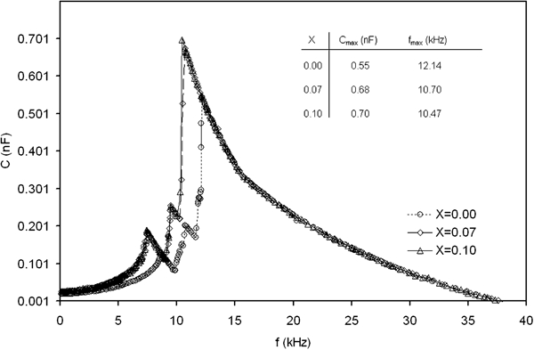
Variation of capacitance as function of frequency of applied ac signal for Bi1·5Zn0·92Nb1·5−xNixO6·92−3x/2 solid solution
Conclusion
In this work, Bi1·5Zn0·92Nb1·5O6·92 pyrochlore ceramics were doped with nickel at different doping ratios. The Ni doping effect on the structural, optical, electrical and dielectric properties of this material has been studied in detail. The XRD analysis revealed a single phase for low doping percentages of x = 0·07 and 0·1. At higher percentages above x>0·1, other phases have appeared. The calculated lattice constants for the single phased samples are found to decrease by doping and reincrease with increasing doping ratio. The optical absorption coefficient, which was recorded in the incident photon energy range of 3·1–5·8 eV, is observed to be strongly affected by doping. The absorption coefficient data analysis revealed an indirect forbidden transition energy band gap of 3·30 eV, which increases to 3·35 and 3·52 eV for a doping content of 0·07 and 0·10 respectively. The widening of the energy gap was attributed to structural modifications. The electrical resistivity of the samples increased with increasing Ni content and increasing temperature, while the pure ceramic pyrochlore reflects typical semiconducting properties and the doped ones reflect very different properties. The dielectric properties of the samples, which were investigated by means of capacitance–frequency characteristics, are observed to have absolute maxima at 12·14 kHz. The increased Ni content slightly increased the dielectric constant of the ceramics.
Footnotes
Acknowledgements
This work was supported by The Scientific and Technological Research Council of Turkey (TÜBİTAK) under grant no. 107M083. The authors would also like to thank the BSc student Mrs B. H. N. Kmail from the Department of Physics, Arab-American University, Palestine, for her help in the electrical data collection.