
Abstract
Indium tin oxide (ITO) ceramic sputtering targets used for the manufacturing of transparent conductive thin films for electrodes in flat panel displays, solar cells, touch panels, antistatic films and others developed and commercially produced are described. Thanks to optimised compositions and developed technology, commercially producing large size planar and new generation rotary ceramic target components have high density (up to 99·5% of theoretical density), uniform microcrystalline structure and superior properties, e.g. low electrical resistivity. As a result, nanosized thin films produced by direct current magnetron sputtering from the developed targets have uniform nanocrystalline or amorphous structures and superior transmittance (>90%) and low electrical resistivity. The morphology and properties of these films have been studied, depending on the film processing features. The benefits of the developed ITO rotary targets for industrial nanosized film processing (e.g. significant increase in process efficiency, about three times higher target utilisation, practically no nodule formation and particle redeposition during sputtering and reduced processing cost) are outlined.
Introduction
Highly transparent and electrically conductive oxide (TCO) thin films are widely used as electrode layers in optoelectronic devices, such as in flat panel displays (FPDs), e.g. liquid crystal displays, organic light emitting diodes, plasma display panels, touch panels, electrochromic devices as well as antistatic conductive films and low emission coatings.1–8 Also TCO films have had a great interest in photovoltaic applications for the formation of flexible thin film solar cells. Along with optical properties, TCO films are used for high temperature strain gas sensors. The films are commonly produced by conventional direct current (dc) magnetron sputtering on glass or polymer substrates, requiring a fine tuned deposition process and high quality sputtering targets. Ceramic sputtering targets are used as a cathode for magnetron sputtering equipment for TCO film processing. Required film properties are defined by compositional and structural features of the ceramics and by sputtering process parameters. The ceramics should be of high purity with a uniform microcrystalline structure. They should possess high electrical conductivity and high density [99+% of theoretical density (TD)] to maximise the useful life of the targets. These characteristics should allow the formation of electrically conductive transparent films without structural defects during sputtering.
One of the most reliable and suitable materials for sputtering targets for the mentioned applications is indium tin oxide (ITO) ceramics because these materials provide highly homogeneous nanostructured or amorphous transparent (>80% of transmittance in optical range) and electrically conductive thin films with thickness of 70–250 nm.4–10 These ceramics are formed by the addition of tin oxide to indium oxide, resulting in modification (distortion) of the crystalline lattice of indium oxide and an increase in its electrical conductivity. The ITO ceramics have a wide direct bandgap (Eg is ∼3·6 eV). The introduction of Sn4+ in In3+ cation sites in the crystalline lattice is balanced by vacancies or O2− sites. This results in the donation of free electrons to the lattice and provides n type electrical conductivity. The content of Sn4+ and the final density of the ceramics are among the crucial factors in the extent of electrical conductivity.9–13 Owing to the presence of lattice defects, such as interstitial atoms or oxygen deficiencies, it is not straight forward to define the theoretical density of ITO ceramics. However, it is generally accepted as 7·14–7·16 g cm−3 for the ITO 90∶10 ceramic composition. This composition (i.e. with an approximate wt-% ratio of 90∶10 between In2O3 and SnO2) is one of the most widely used in the industry since it provides the high quality conductive and transparent films required for optoelectronic applications. However, some other ITO compositions with ratios from 98∶2 to 80∶20, such as 98∶2, 97∶3, 95∶5, 85∶15, 80∶20 and others, are used, depending on the customers’ requirements in similar and other optoelectronics devices.
The quality of dc magnetron sputtered thin films is generally superior when ceramic targets have higher density; higher density targets also display an enhanced deposition rate.14, 15 Dense ceramic targets have higher resistance against sputtering erosion and nodule formation. In particular, nodules (‘black spots’), which are considered as indium suboxide In2O,16–18 occur during sputtering on the periphery of the erosion race track on target surfaces and tend to cause electrical arcing. The presence of nodules reduces the film processing efficiency and deteriorates the homogeneity and properties of the films, and they must be periodically removed during processing. The nature of nodule formation is complex, and its mechanism has not yet been completely understood.16–21 However, based on the experimental results, Gehman et al.14 noted that high ceramic target purity is not the major property that promotes films with lower resistivity, i.e. ultrahigh purity grade targets would be only a small advantage to the film quality. Similarly, a small influence of ITO ceramic density on electrical resistivity and transmittance is noted by Yoshimura et al.15 when the density is above 92–95% of TD. This is also confirmed by Zhang et al.,22 who studied RF sputtering in later publications. The authors16, 21, 22 suggest that sputtering parameters may have a greater influence on the film quality and nodule formation when using rather high density and uniform ceramic targets.15 Additionally, target design and ceramic to metal bonding quality are also important for the sputtering process efficiency and film quality. However, in accordance with industry needs, in order to maintain stable, without downtime, dc magnetron sputtering processing of high quality thin film, high density (99% of TD or greater) and large size ITO ceramic products are required.
The development and characterisation of ITO and some other In2O3 based ceramics are of the interest of many ceramic manufacturers and TCO consumers. Despite numerous studies, there is not enough data describing the manufacturing and properties of commercially produced ITO ceramics. In reality, there is a big ‘distance’ between the requirements for laboratory scale samples and industrial ITO targets and their actual manufacturing. The challenges in the manufacturing of ITO sputtering targets include the use of high quality starting materials, especially In2O3 powders with respect to purity, morphology and sinterability, manufacturing routes and sintering process. Basically, the purity of ITO ceramics affects the quality of the deposited films (e.g. electrical conductivity and transmittance) and the sputtering behaviour of the targets. The purity of ceramics is defined by the quality of starting materials, batch composition and accuracy of ceramic manufacturing. Also the film quality is dealt with the homogeneity of distribution of SnO2 in In2O3 in ceramics that is defined by ceramic processing. Densification is one of the critical points in manufacturing ITO bodies with maximal density; it is defined by starting material properties, features of the processing route and firing conditions. In2O3 based ceramics generally have a low sinterability. This is related to the partial dissociation and volatilisation of In2O3 and SnO2 at elevated temperatures in accordance with the following reactions23–25


The present work summarises the development, optimisation and industrialisation of the state of the art technology of ITO ceramic large size planar and relatively new rotary targets using in-house prepared In2O3 powders. ITO ceramic tiles with areas of up to 1200–1700 cm2 (with a variety of dimensions) for planar targets and ITO hollow cylinders with diameters of 100–200 mm and a wall thickness of 4–10 mm, which are assembled into rotary targets with a length up to 3·8 m, are currently manufactured. Properties of the commercially manufactured ITO ceramics and the nanosized films obtained from these ceramics deposited by dc magnetron sputtering are reported; the film properties are analysed as a function of sputtering conditions.
Sputtering target design and its influence on thin film processing
Owing to the present need of high quality films in large area optoelectronic devices, ceramic targets are required to be as large as possible. Until recent time, only planar sputtering targets were used in the industry. These targets consist of several dense monolithic tiles, which are assembled and bonded onto a metallic backing plate. Large size tiles with areas of up to 1400–1700 cm2 are demanded to minimise the number of joints in a target surface. The manufacturing of these large sized fully dense products is quite challenging for commercial ceramic processing. However, the conducted development allowed implementing into production these large tiles with up to 99·5% of TD.26
Conventional planar targets are eroded during sputtering, resulting in a specific racetrack pattern (localised plasma zone). Only 20–40% of the planar target is utilised. Moreover, the risk of formation of nodules on the surface of the targets, which finally leads to disruption of the film deposition, is relatively high.16–21,26 Thus, the need for system maintenance during target lifetime, which reduces the system up time, is inevitable using a planar cathode configuration.
In order to increase both utilisation of expensive ITO ceramic sputtering targets and efficiency of the sputtering process, rotary sputtering cathodes equipped with tubular ceramic targets may be employed.27, 28 Such rotary sputtering targets are regarded as a new generation of sputtering targets used for TCO thin film preparation. A schematic of rotary and planar targets is shown in Fig. 1. As opposed to planar targets, almost the entire surface of rotary targets becomes a working surface that results in a significant increase in target utilisation (typically 70–90%, depending on the magnet array or about three times greater than the utilisation of planar targets). Erosion of the quasi-entire surface area also avoids undesired particle redeposition on the target surface, so the growth of nodules can be avoided or, at least, significantly suppressed. Moreover, because the thermal load is on the entire cylindrical target surface area with rotary magnetrons, higher power loads can be applied on rotary targets. This normally leads to higher deposition rates. All these features provide a significant reduction in the thin film production cost, and a longer service cycle may be achieved.
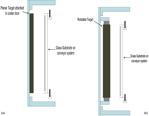
Schematic of a planar and b rotary sputtering targets design
Recently introduced rotary sputtering targets consisting of tubular metal substrates coated with ceramic powders used for TCO thin film preparation (e.g. ITO) are produced by employing high temperature processing, such as plasma spray coating and some other methods.28 However, these designs and processing methods do not allow to obtain high density ceramic layers (limited to only 90–95%) with a necessary thickness; typically, only 2–3 mm may be obtained by these technologies, while 4–10 mm after post-firing machining are typically required for planar targets in the industry. Also the ceramic layers of the targets formed by these methods cannot be easily separated from a metallic substrate that creates difficulties in recycling expensive ITO materials. The use of rotary targets with hollow cylindrical segments made by ‘traditional’ ceramic processing bonded to a metallic backing tube can significantly reduce these difficulties. However, ITO rotary sputtering targets were not widely used in the optoelectronic industry until recent time due to the serious complexity in ITO ceramic component manufacturing. It is especially regarded to rotary targets based on thick wall dense ITO ceramic hollow cylinders because they did not exist. Our recent development has allowed implementing the technology of ITO ‘ceramic’ rotary targets to the TFP industry, significantly increasing the process efficiency.29
Experimental
Starting materials and manufacturing
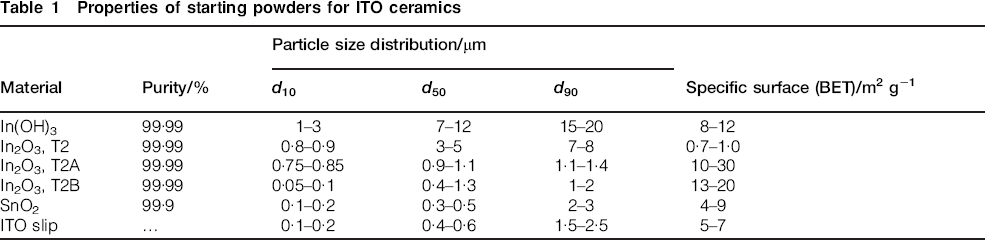
High purity commercially produced In2O3 and SnO2 powders are used as the main starting materials for the production of ITO ceramics. The In2O3 powders are in-house manufactured using a proprietary process from pure indium via acidic dissolution with subsequent neutralisation and precipitation of In(OH)3. The obtained In(OH)3 is then calcined at proper temperatures specially selected to obtain In2O3 with desirable powder characteristics and morphology. When hydrochloric acid is used for acidation, the In2O3 powders prepared via this route are denoted as T2. Also the starting powders with higher specific surfaces and ‘special’ morphologies were prepared by modification of the precipitation and calcination processes. Processing ‘waste’ materials and spent targets after sputtering are recycled on the conventional basis to obtain pure In. Each lot of starting In and prepared In salts, In(OH)3 and In2O3 powders is qualified by chemical analyses and powder characterisation. In2O3 powders, as a major ingredient of ceramic compositions, are produced with 99·99% purity. This is achieved through the multistep process control of the In2O3 preparation. Typical properties of the processed powders are summarised in Table 1, and their typical particle size distributions are illustrated in Fig. 2. The In2O3 powders have a cubic morphology, and they are generally aggregated (Fig. 3). The properties of SnO2 powders manufactured by other suppliers are also shown in Table 1.
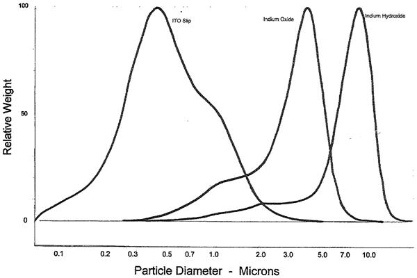
Particle size distribution for In(OH)3 and In2O3 powders and ITO slip
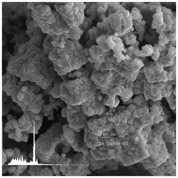
Image (SEM) of In2O3 type 2 powder
Properties of starting powders for ITO ceramics
The weight ratio between In2O3 and SnO2 is selected to optimise the electrical properties of the ceramics and the electrical properties and transmittance of the films. Based on numerous studies and practical experience, including the end users requirements, the ratio of 90∶10 generally provides the optimal combination of low electrical resistivity and high optical transmittance of films prepared by sputtering, and this composition is mostly used in the industry at the present time.1–4,7–10,14,17–22,26,29 Because of this, the major studies described here were conducted for ITO 90∶10; however, some other ITO ceramic compositions used for optoelectronic industrial applications were also studied.
Starting materials are mixed and milled using ball milling or attrition milling processes in accordance to specially designed procedures. Attrition milling allows adequate disintegration in significantly shorter time. The formulated water based ceramic slurries (special dispersing and binding agents have been selected for the slurry preparation) have workable viscosities and specific gravities suitable for consequent ceramic processing steps. The ceramic bodies are shaped using a proprietary processing to produce either flat tiles of various dimensions or hollow cylindrical bodies. After gentle drying and dry state cutting (if required), ‘green’ ceramic bodies are fired in high temperature electric kilns using specially designed kiln loading and firing conditions. The optimised firing profile (firing temperature <1600°C) and firing conditions provide near complete densification (up to 99·5% of TD). Fired ceramic bodies are cut and ground with diamond tooling in order to attain precise dimensions, flatness or roundness (depending on shape) and surface quality, which are required for back face metallisation, bonding and sputtering processes. For example, roughness Ra of the ground ceramics is attained at <1 μm. Multistep process control during powder preparation and ceramic manufacturing ensures high purity and high quality ceramic targets. Ground ceramic components are ultimately bonded to a metallic backing plate or tube. Dye penetration and ultrasonic non-destructive testing, which may be conducted for bare ceramics and bonded targets, confirmed the absence of cracks, flaws and other defects, which might negatively affect the sputtering behaviour.30 Examples of large size planar and rotary targets and their constituents manufactured are illustrated in Fig. 4.
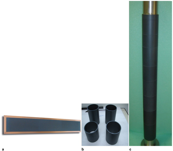
Indium tin oxide ceramic sputtering targets commercially produced:
Sputtering
ITO films were deposited from planar and rotary ITO ceramic targets, including from the targets with actual dimensions used for industrial applications, onto glass substrates (Corning no. 1737F) using industrial dc magnetron sputtering systems in collaboration with designated sputtering equipment companies. The base pressure, power density and sputtering pressure in the process module during the sputtering runs were typical for industrial applications. The base pressure in the process module was <5×10⁻⁵ Pa. Typically, a power density of 3·1 W cm−2 for planar targets and two to three times higher for rotary targets was applied during the sputtering runs. The sputtering pressure was in the range of 0·3–0·6 Pa and could be adjusted using a mass flow controller. Specifically, for rotary targets, different sputtering powers from 5 up to 12 kW were applied with a total energy of greater than 3000 kW h, and sputtering behaviour (e.g. plasma behaviour, arc formation, cycling performance, film uniformity) was evaluated. The sputtering process was run in an Ar atmosphere with the addition of 0–5% of O2 reactive gas. The sputtering was conducted at ambient and elevated temperatures, i.e. on the preheated substrate (up to 200–235°C); IR radiation lamps installed in the process module were applied to maintain uniform substrate heating. Post-deposition heat treatment (annealing) of the coatings produced at ambient temperature was carried out using an electric furnace in an air atmosphere. Annealing was carried out at temperature of 200°C over 60 min. The parameters of the sputtering process were optimised in order to obtain high quality films, depending on particular conditions.
Characterisation
Particle size distribution of processing powders was measured using the Sedigraph and CPS Disc Centrifuge instruments; specific surface area was measured with the Brunauer–Emmett–Teller (BET) method. The morphology of the powders was studied by scanning electron microscope (SEM). The phase composition and microstructure of the fired ceramics and sputtered films were studied using glancing incidence angle X-ray diffraction (XRD) as well as SEM and transmission electron microscopy under different magnifications using ‘as received’ or etched samples. Slurry characterisation was conducted using conventionally used methods by determination of viscosity (Brookfield viscometer), specific gravity and pH. Thermal gravimetric analysis (TGA) was conducted in the range of 20–1400°C using a standard procedure. Oxygen content in the ITO ceramics was determined using TGA. This method is based on the calculation of the weight decrease after reduction in the pulverised sintered ITO ceramic powder since it is assumed that the weight decrease is equivalent to the oxygen content in ITO when In and Sn are fully reduced.
The density of ceramic components was measured by the water immersion method based on Archimedes’ law. Young's modulus was tested using the resonant frequency method in accordance with ASTM C885. Sonic velocity was determined based on the formula related Young's modulus and sonic velocity: E = c2d(1+p)(1−2p)/(1−p), where E is the Young's modulus, c is the sonic velocity, d is the density and p is the Poisson's ratio also determined by ASTM C885. Flexural strength (four-point loading) was tested in accordance with ASTM C1161. Thermal diffusivity α was measured by the laser flash technique in accordance with ASTM E1461. Specific heat (heat capacity) Cp was tested using a differential scanning calorimeter (ASTM E1269). Thermal conductivity λ values were calculated using the formula: λ = αCpd (where d is density). Thermal properties were determined in the temperature range of 20–250°C. Coefficient of thermal expansion (CTE) was determined in the temperature range of 20–1000°C using a quartz dilatometer. Specific electrical resistivity was determined using the inline four-point probe measuring unit. Test ceramic samples were cut from actual tile targets for the dimensions required by the appropriate testing procedure.
ITO film thickness was optically determined using a reflectometer analyser (J. Y. Horiba, Tokyo). Film uniformity was determined by comparison of the thickness, measuring at different points of the film samples. The microstructure and phase composition of the films were studied using SEM and XRD techniques respectively. The specific electrical resistivity of the films was determined using a four-point probe measuring unit (Jandel Scientific, Corte Madera, CA, USA). Transmittance in the visible range from 400 to 800 nm wavelength was measured using a spectrophotometer (PerkinElmer, Norwalk, CT, USA). Film stress was determined for the selected films deposited onto Si wafers of 100 mm diameter in accordance with a standard procedure for FPD applications using a cantilever technique; an α-step profilometer was used to measure the bending contour due to the stress in the thin films.
Results and discussion
ITO ceramics
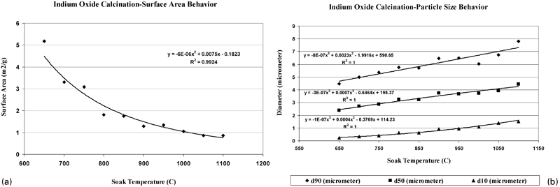
The developed technology of ITO ceramics includes optimised colloidal processing using high purity starting materials, advanced shaping technique and optimised firing process, which are the company ‘know how’. In addition to the chemical routes of the starting material preparation, the calcination process, e.g. calcination temperature and conditions, may be one of the ‘tools’ that may be used to manage In2O3 powder characteristics and morphology. Figure 5 illustrates the influence of calcination temperature on In2O3 T2 powder characteristics. It is clearly seen that particle size increases and specific surface area decreases with the increasing calcination temperature. Accordingly, varying the calcination temperature and calcination conditions, the ITO slurry preparation, e.g. dispersion and slurry composition, milling process, etc., may be successfully managed. The ITO ceramic slurry composition and colloidal process development provided low viscosity with a relatively high specific gravity and a proper pH level of the slurries. The starting powder properties and the dispersant–binder system selection, as well as the slip preparation process, could overcome the possible difficulties in a tendency to agglomeration due to the increased attractive van der Waals forces, achieving adequate slip rheological properties and providing uniform distribution of SnO2 in In2O3. The obtained ITO slips have approximate solid contents of up to 84 wt-%, and owing to their parameters, they are suitable for different forming processes. Various shapes of ceramic bodies with quite large dimensions are produced. The material preparation process and shaping methods allow to reach green densities of the ceramic bodies of 65–70% of TD. This high level of green density promotes densification and relatively low grain growth at sintering.
Influence of calcination temperature on In2O3 T2 powder parameters:
Densification of ITO ceramics depends on the properties and morphology of the starting materials, composition, e.g. a weight ratio of In2O3/SnO2 in the mix, ceramic processing route and firing conditions. As noted above, In2O3 based ceramics generally have a low sinterability that is related to the partial dissociation and volatilisation of In2O3 and SnO2 at elevated (above 1200°C) temperatures.23–26 Partial volatilisation of the oxides at elevated temperatures was confirmed by the results of TGA (Fig. 6). Owing to this fact, a temperature increase might not assist a full densification if appropriate conditions are not maintained. The use of sintering aids must be strongly limited due to the requirements of high purity of ITO ceramics and films. In the case of the use of expensive and not very productive hot pressing or other pressure assisted firing technologies, which also have a limitation for manufacturing large size ceramic components, some lack of oxygen takes place that inhibits densification of ITO ceramics to the required high level, i.e. the pressureless sintering process may be the most reasonable for ITO ceramics, particularly large size and different shape components. The option to apply pressure at the intermediate step of the sintering proposed by Son et al.31 may be interesting only for very small size bodies, and it is not practical for industrial manufacturing of large size bodies, especially of the hollow cylindrical shapes required for rotary targets (actually, the authors31 conducted their studies with ∼10 mm diameter tablets using the dilatometric analysis equipment).
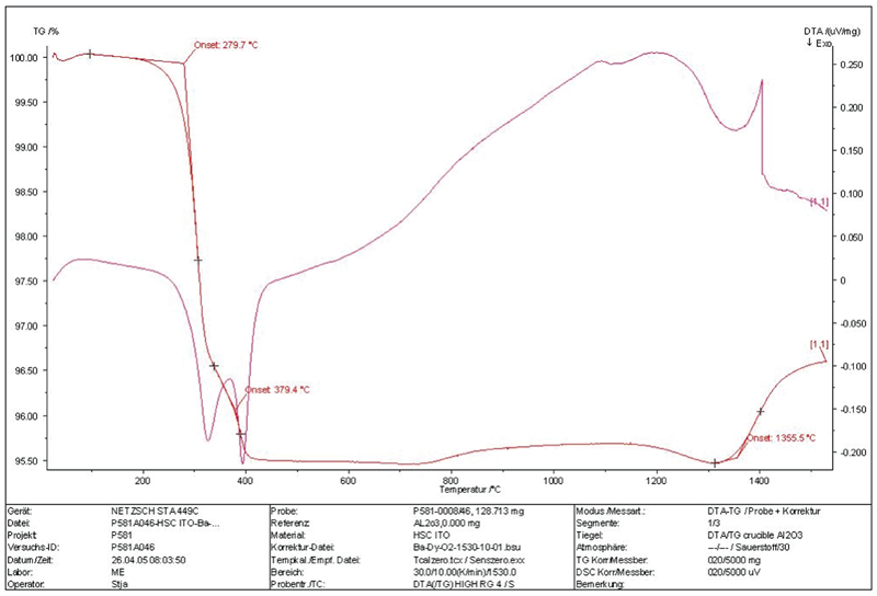
TGA curve of ITO (90∶10) ceramics
Based on the studies of the influence of the morphology of In2O3 powders on their sinterability, it was found that particles with a cubic shape provided the highest sinterability of ITO ceramics; the presence of particles of other shapes (e.g. due to some imperfectness of the In2O3 preparation) in sufficient quantities resulted in the decrease in ceramic sinterability. This is in a good correlation with the study conducted by Kim et al.,32 who found that the transformation of rhombohedral In2O3 to cubic induces coarsening of grains and formation of voids in the microstructure that can retard ceramic densification. A proper combination of starting powders with specially selected particle size distribution and specific surface area, including the use of powders with rather high specific surface, can improve the sinterability of ITO ceramics without sacrificing the capability to process large size products. General parameters of In2O3 powders, which may be utilised in ITO processing, are performed in Table 1.
Because the evaporation–condensation mechanism inherent to In2O3 and SnO2 based ceramics is not favourable for high densification, this negative factor has to be overcome at ITO sintering. ITO ceramic formation occurs via solid state sintering. High temperature densification and grain growth occur through the recrystallisation process due to ‘necking’, as the intermediate stage, and grain coalescence (through grain boundary diffusion). Also the diffusion viscous flow of the vacancies, which are presented in the system due to the lattice defects occurring when Sn4+ penetrates in the In3+ cation sites in the crystalline lattice, promotes ITO densification. Grain growth is rather sufficient (Figs. 7 and 8), which is generally beneficial for porosity elimination as the pore configuration becomes energetically unstable with a decrease in the number of grains surrounding a pore.33–36 However, the grain growth in the existing situation is not very high (in comparison with the sintering of ITO ceramics from nanopowders31, 37, 38) that is favourable for manufacturing large size components. If a secondary phase (In4Sn3O12) occurs, it is growing on the grain boundaries, filling the space between the grains (mostly, at the ‘triple junction’ locations). For the well sintered ceramics (i.e. with density of 99% of TD or higher), occasional pores may be found between grains mostly at the ‘triple junction’ locations. As a positive point, there are practically no pores inside the grains.
Microstructure of ITO 90∶10 ceramics (image from fracture surface without thermal etching); sample for examination was cut from actual large size cylinder
Microstructure of ITO 95∶5 ceramics (demonstrating grain boundary area)
A specially designed firing profile and selected firing conditions provide a high sinterability of ITO ceramics without applying pressure at elevated temperatures. The density of ITO ceramic bodies (tiles and hollow cylinders) fired in industrial conditions reached up to 7·13 g cm−3, i.e. up to 99·5% of TD (considered as 7·15–7·16 g cm−3), with a good reproducibility. The achievement of high density values strongly depends on the size of the products and firing conditions. These high density values could be achieved not only for rather small tiles with areas of 500–900 cm2, but also for tiles with areas of up to 1200–1750 cm2 and for hollow cylinders with wall thickness of 10–15 mm (before grinding).26, 29 Firing of cylinders has an additional difficulty related to their substantial mass and the requirement of an accurate shape with minimal ovality. To overcome these difficulties, firing has been engineered in accordance with the general principles in ceramic processing utilising the understanding of the processes occurring with ITO components and taking into consideration their large size and mass as well as the industrial kiln design. The proposed and tested rapid rate sintering for nanocrystalline ITO37, 38 is not suitable for large size components, which need to be obtained with density of up to 99%+ of TD. It is clear that, due to the sufficient difference in sintering rate and shrinkage of the outer and inner areas of the ceramics and due to some differentiation of the heat and gas transfer in real production furnaces, the fast firing is not safe. Additionally, Kim et al.37, 38 demonstrated that fast firing did not provide the desirable densification, even when more ‘active’ nanopowders were used because the densified outer region formed constrains densification of the inner region, and that was especially sensitive with the sample mass increase.
The ITO ceramics studied in this work consist of mostly cubic In2O3 (bixbyite) as the major crystalline phase. However, in accordance with XRD analysis, the presence of a secondary phase In4Sn3O12 in ITO 90∶10 and 80∶20 ceramics is observed. This correlates with the data from the publications, which regards to the presence of this phase in the ITO ceramics with a content of 6 at-% or more of Sn.18,39–43 The content of this phase has not been accurately determined, and it depends not only on the composition (ceramics with higher contents of SnO2 have higher contents of the secondary phase) but also on the firing conditions. In many cases, the detection of this secondary phase can be difficult since its peaks in the difractograms are overlapped with the peaks of the major In2O3 phase. Some authors claimed the possibility to obtain ITO ceramics with a single phase structure.44 They used a co-precipitation technology of the starting powder preparation that provides a high level of homogenisation of In2O3 and SnO2. However, these authors did not demonstrate actual ceramics with only In2O3 phase. In accordance with our studies, as well as with the results of other authors,18, 32, 42, 43 even the coprecipitation method of the starting powder preparation cannot guarantee the absence of the secondary In4Sn3O12 phase in ITO ceramics; however, this approach can promote minimisation of this secondary phase formation and its more even distribution in ceramics. The formation of this In4Sn3O12 phase initiates from the SnO2 grains, and it is clear that more even SnO2 distribution reduces the growth of the In4Sn3O12 phase. The formation of this secondary phase may be regarded as positive from the densification standpoint because this new phase grows between In2O3 grains occupying residual pores. Owing to the formation of the In4Sn3O12 phase, it is much easier to obtain density values of 7·10–7·14 g cm−3 for the 80∶20 composition, although the calculated TD of this composition is slightly lower. Crystallisation of the SnO2 phase was not detected, which is in agreement with other studies.19, 24, 39, 40
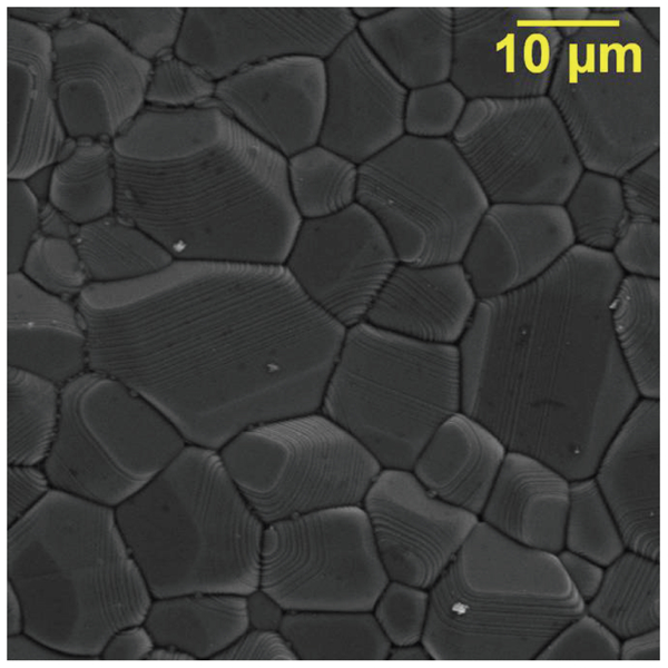
The microstructure of the produced ITO ceramics is dense, rather uniform, and it consists of grains with sizes from 2 to 20 μm, depending on the ITO composition (Figs. 7–9). The grains consist of crystallites with sizes of around 50–100 nm (which vary depending on starting material preparation conditions), as determined by XRD analysis using the Scherrer formula. The secondary phase formation inhibits grain growth that may be confirmed by the comparison of grain sizes of the studied materials. As can be seen from the SEM images, the grain sizes of ITO 95∶5 ceramics, which does not contain the secondary phase, are 10–20 μm (Fig. 9a), while ITO 90∶10 (Fig. 9b) and 80∶20 (Fig. 9c) ceramics containing this phase have smaller grain sizes (5–10 up to 15 μm, and 2–7 μm respectively). The grain cleavage can be seen in the SEM images of fracture surfaces. This provides evidence of a high extent of ceramic densification since the fracture occurs through the grains. Irregular occasional small intergranular pores are uniformly distributed, but they are not interconnected. It may be noted that, in the case of manufacturing large size products, the firing profile is usually extended in accordance with the general ceramic principles that result in more intensive grain growth.
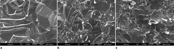
Comparison of microstructures of ITO ceramics:
Appropriate oxygen content in ITO ceramic targets is important to maintain a stable sputtering process and a wide ‘process window’ required for consistency of the producing films. Depending on the process features, either fully oxidised or partially reduced ITO tiles are preferable. The theoretical oxygen content in ITO ceramics is not a very reliable value because it depends on the method of calculation. This value may be 17·682% for ITO 90∶10 if it is extracted from the mixture of 90 mass-%In2O3 and 10 mass-%SnO2, or 17·243% if it is calculated from the composition (In0·907Sn0·093)2O3, where some amount of Sn atoms substitute In atoms in the crystalline lattice. Owing to the presence of a secondary In4Sn3O12 phase, the oxygen content becomes even more uncertain. For our study, an oxygen content of 17·69% was considered as theoretical for ITO 90∶10, 18·08% for ITO 80∶20 and 17·48% for ITO 95∶5. As noted, the oxygen content determination was conducted using TGA analysis. The determined oxygen content of the studied ITO 90∶10 ceramics is in the range of 17·55–17·90%, which is close to the theoretical value taking into account the measuring accuracy. In fact, the difference in actual and theoretical oxygen contents for the 80∶20, 90∶10 and 95∶5 ITO compositions is higher for compositions with lower In2O3 contents (for comparison, the actual oxygen contents for 80∶20 and 95∶5 compositions are 17·94 and 17·43% respectively). There is not a clear correlation between oxygen content values and densities of ITO ceramics when their densities are greater than 98·5–99% of TD. It is also difficult to explain the variation in the values of oxygen content when the actual oxygen contents for some samples are even greater than the theoretical value. Most likely, the answer can be found considering the grain boundaries in ITO ceramics.
The physical properties of the produced ITO ceramics are listed in Table 2. Their mechanical strength is at a moderate level; however, ITO ceramics are not intended for structural applications. Young's modulus and sonic velocity, in addition to structural properties, indicate the level of densification, especially in the presence of closed pores and macrodefects, and these data are useful for comparison of ceramics with the same composition, e.g. ITO materials. However, the determination of sonic velocity using the above mentioned formula may not be accurate enough for ITO ceramics because of a relatively wide range of Poisson ratio values.
Some physical properties of studied ITO ceramics
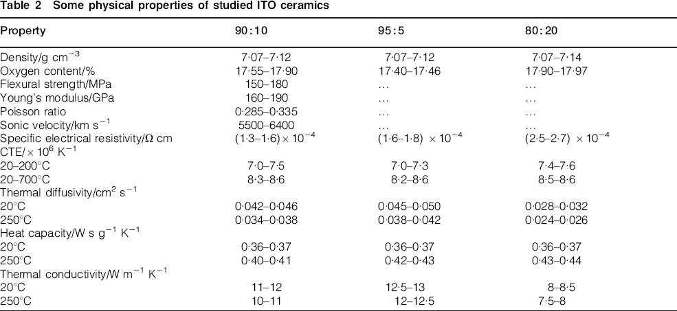
The values of specific electrical resistivity of ITO ceramics are generally lower for the 90/10 compositions in comparison with some others. The values range from (1·3–1·7)×10−4 Ω cm for the compositions of 90∶10 to (2·5–2·7)×10−4 and (1·6–1·8)×10−4 Ω cm for the 80∶20 and 95∶5 compositions respectively. However, the measure of electrical resistivity is not a very reliable indicator of ITO composition, especially if the SnO2 content is in the range of 5–12%. Densification of ITO ceramics has more influence on the electrical resistivity (ceramics of the same composition but with higher density usually demonstrate lower values of specific electrical resistivity) than their ultrahigh purity. However, a high total content of impurities (e.g. more than 1000 ppm) may result in not only the undesirable distortion of the In2O3 crystalline lattice, but also the formation of electrically insulating layers between In2O3 grains. This may enhance the ceramic electrical resistivity and, consequently, the film resistivity. In this case, the consideration of impurities and their influence on the electrical properties of ITO ceramics should be ‘selective’, e.g. the formation of alkali silicate, alkali earth silicate or some other glassy phases should be avoided. At the same time, some other impurities do not affect the electrical properties of ITO ceramics.
The values of electrical resistivity for ITO ceramics may vary in a rather wide range, depending on the content of the less conductive In4Sn3O12 phase. This phase, as discussed above, is formed when Sn contents are >6 at-%. This phase content and the solubility of Sn in In2O3 may depend on processing features, such as particle size of starting ingredients, mixing, milling and firing conditions (e.g. temperature distribution in the kiln, oxygen level, etc.). Practically, an oxygen level and the sintering process also depend on the size of the ITO ceramic bodies, their loading in the furnace and the ‘thermal mass’ in the furnace (related to the products sizes and their amount in the furnace), which may vary from firing to firing under actual production conditions. Depending on these factors, the content of the In4Sn3O12 phase and electrical conductivity of the ceramics may vary. Elevated values of electrical resistivity in the 80/20 composition are explained by the crystallographic structure of the material and a greater extent of the slightly less conductive In4Sn3O12 phase. However, the presence of this In4Sn3O12 phase positively affects the density values of ITO ceramics. Therefore, the influence of the phase composition and structure of ITO ceramics on their properties and quality of sputtered films is rather complex.
It is difficult to correlate the influence of microstructure (grain size and grain size distribution) on the electrical properties of ITO ceramics. There is no discussion in the publications regarding this influence, even for small samples processed and fired under very uniform laboratory conditions. Considering real production conditions with possible variations in starting powder preparation and firing conditions, the structure may vary from firing to firing, especially if large sized products are fired. The influence of the microstructure on the electrical properties may be difficult to observe. Only a small increase in conductivity with a grain size growth might be noticed.
Thermal diffusivity and thermal conductivity of ITO ceramics have to be as high as possible to minimise thermal tensile stresses, which naturally occur in targets during sputtering; otherwise, related defects may be a cause of non-uniform deposition of ITO films. The values of these properties are higher for materials with higher contents of In2O3. The influence of ceramic densification on the thermal properties is similar to its influence on electrical conductivity; the higher the density, the greater the thermal diffusivity, the heat capacity and the thermal conductivity. Samples with higher electrical conductivity also demonstrate higher thermal conductivity. The values of thermal diffusivity and thermal conductivity decrease with a temperature increase. The change of thermal conductivity versus temperature has a linear character, but the change of thermal diffusivity with temperature does not display such behaviour (Fig. 10). Both electrical and thermal conductivities tend to be higher for ITO samples with larger grain sizes, since ceramics with larger grains contain fewer grain boundaries to act as resistance to electrical and thermal flow (with respect to electrical properties, this trend may be noted for samples with a significant difference in grain sizes). The values of CTE of ITO ceramics with different contents of SnO2 are comparable, which allows the use of similar compositions for metallisation and bonding processes.
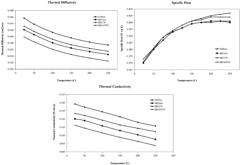
Thermal diffusivity, heat capacity and thermal conductivity of ITO 90∶10 ceramics
ITO thin films
Thin films with a thickness of 70–150 nm obtained by conventional dc magnetron sputtering at different conditions were analysed for their compositions, microstructure and properties. The results for the films obtained from 90∶10 ITO ceramic targets, considered as the most reliable composition, are reported. By adjusting the amount of oxygen inserted to the system, as well as other sputtering parameters, a wide process ‘window’, a stable sputtering process and high quality layers were obtained.
The obtained thin films had a uniform thickness; the film uniformity was determined optically by measuring the thickness in various points over the large area of the substrate. The thickness difference between points of measuring was below 10%, which is well accepted in the optoelectronic industry. The roughness of the films deposited at elevated temperature and after annealing was about 2 nm; this high film uniformity was obtained from both rotary and planar targets (Fig. 11).
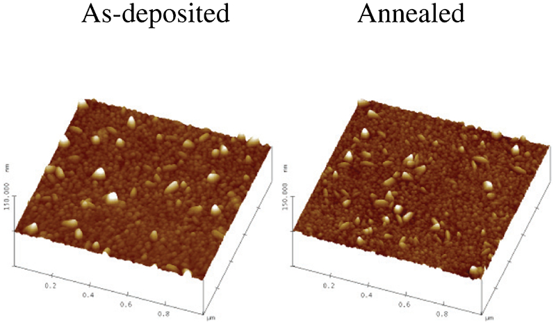
ITO coating topography: left: as-deposited; right: annealed film (coating roughness: Ra ∼2 nm, Rmax ∼22 nm)
The glancing incidence angle XRD spectra of selected ITO layer structures were recorded and compared with JCPDS database no. 6-0416. The spectrum of an almost entirely amorphous structure (a-ITO) with a small amount of crystalline site was inherent to the ITO films deposited at room temperature (‘as deposited’), as demonstrated at Fig. 12. A polycrystalline structure (p-ITO) spectrum showing Bragg lines of the cubic In2O3 phase with preferential orientation in the (222) direction (Fig. 12) was formed in the films produced with thermally activated processes. A rather small diffraction peak corresponding to the (440) orientation was also detected. This film structure, depending on the sputtering conditions, is in good agreement with other studies.45–50 At low 2θ angles (20–35°), the signals from the layers are superimposed with the X-ray amorphous spectrum of the glass substrate.
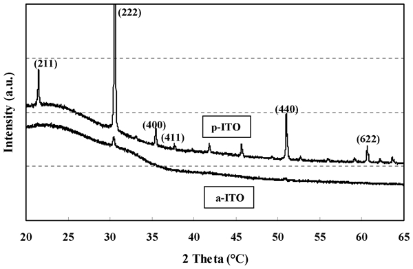
XRD spectra of ITO (90∶10) films obtained at different sputtering conditions (for amorphous and polycrystalline films)
Morphology studies easily demonstrated the influence of sputtering conditions on the ITO film structures. The micrographs of a-ITO (‘as deposited’) films showed a poor topographical contrast. A polycrystalline structure of cubic In2O3 grains was observed for the films deposited at elevated substrate temperatures. The films produced after annealing at 200°C also had very homogeneous polycrystalline structures (p-ITO) consisting of the In2O3 phase. These crystalline structures exhibited densely packed equiaxed (cubic) grains with average sizes of 10–25 nm (Fig. 13). Occasional nanopores were observed at some triple junctions between grains. The evolution of some columnar grains with size of 30–50 nm that form larger domains may also be seen in Fig. 13. Such patterns are typical for heat treated and elevated temperature deposited ITO films.45, 46 The XRD and microstructure studies verified that the annealing process thermally activated complete crystallisation of the amorphous film structure and, subsequently, promoted a density increase in the ITO films.
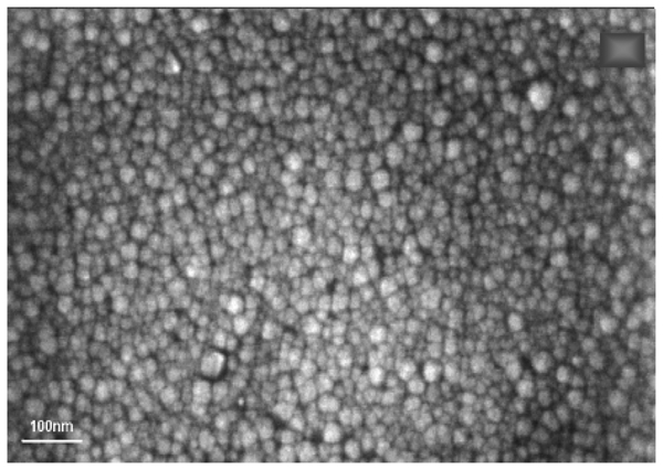
Microstructure of ITO (90∶10) film prepared by dc magnetron sputtering (deposition at room temperature with subsequent annealing at 200°C during 1 h)
The specific electrical resistivity of the amorphous (‘as deposited’) films was as low as ∼600 μΩ cm at the oxygen flow of approximately 1·6% (Fig. 14a). After annealing, the specific electrical resistivity of the nanocrystalline ITO structures was lowered to 200–210 μΩ cm, which is well acceptable for various FPD applications. Transmittance of the layers at 550 nm wavelength was approximately 85% with insertion of approximately 1·8% of oxygen for ‘as deposited’ films; transmittance was increased to more than 90% after 1 h annealing in air (Fig. 14b). The results are in a good agreement with previous studies46–51 when an annealing process results in a relaxation of disorder bands as well as crystallisation of the amorphous network, thus increasing the electrical conductivity and optical transmittance of the film. Deposition on a heated substrate provided the same level of specific electrical resistivity and transmittance as the annealed films due to crystallisation on the hot substrate.
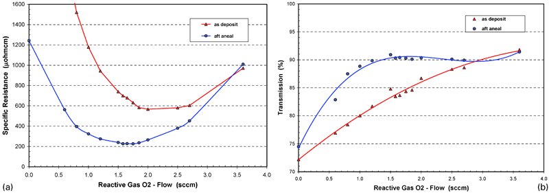
Properties of ITO films prepared from ITO 90∶10 ceramic target by dc magnetron sputtering (after deposition and after annealing at 200°C during 1 h):
Selected film samples obtained from spattering using planar and rotary targets were evaluated for their stress condition. The ‘as deposited’ films are considered as being under compressive stress. It was assumed that compression of the ‘as deposited’ films stemmed mainly from the thermal expansion mismatch between the ITO layer and the Si wafer substrate.49 After the post-deposition annealing of the amorphous ITO film, the film stress converted from compression to tensile. Values of approximately −200 MPa (i.e. compressive stress) were determined for the as deposited 150 nm films, while values of approximately +(200–250) MPa (tensile stress) were determined for thin films after annealing. The transition of compressive stress in a-ITO to tensile stress in p-ITO after annealing may be due to an enormous densification, as an amorphous structure transforms to crystalline phase with nanometric grain sizes. The obtained values are within the specifications for the stress conditions for the FPD applications (below than ±500 MPa compressive/tensile49).
It was difficult to define a strong correlation between the density of ITO ceramics and the macroscopic properties of the ITO films. Based on the studies conducted by Utsumi et al.,9, 10 an increase in density of ITO ceramics from 90 to 99% of TD resulted in a slight decrease in film resistivity due to a slight increase in carrier concentration. This change of resistivity was noted when the density of ceramic samples increased from 97 to 99% of TD; however, an influence on film transmittance was not found. Yoshimura et al.15 also did not find film property improvement with a ceramic density increase of >92% of TD. These authors also indicated that an increase in substrate temperature to 300°C during sputtering allows the use of lower density ITO targets. However, it should be noted that all samples used for the sputtering tests in the present work had a high level of density (99% of TD or greater) that is required by the FPD industry. This high level of density of ceramics has to be maintained in order to not only achieve high quality film properties but also minimise the occurrence of defects in the films and maximise the sputtering efficiency in industrial conditions, especially in the case of large area targets.
Extensive sputtering tests (with total sputtering energy greater than 2500 kW h) of new rotary sputtering targets consisting of high density ITO hollow cylinders with medium size inside diameter (135 mm) and wall thickness of 6 mm bonded to the titanium backing tube with a total length of the ceramic component of 1200 mm demonstrated well acceptable results, including adequate film properties (e.g. electrical resistivity and transparency) comparable with those obtained by sputtering of planar targets under standard conditions and that satisfy industrial requirements.52 Owing to rotation, utilisation of the ceramics was significantly higher; practically, the whole target was spent with a thickness of the remaining material even <1·5 mm for the almost entire length. Based on the erosion profile obtained after the sputtering of this relatively ‘short’ rotary target (Fig. 15), it can be noted that utilisation of the target can be minimum 80%. Later manufactured longer rotary targets with length of 3–3·8 m allowed increasing the utilisation even over 90%. No defined erosion groove (‘race track’) inherent to planar targets appeared. Films with thicknesses in the range of 70–100 nm had a high uniformity with deviation of <10% that is well accepted for optoelectronic industry and comparable with a uniformity of films prepared using metallic rotary targets. A stable behaviour was observed during the cycling process when the plasma was exposed to OFF and ON modes for several hundred times in order to test real manufacturing conditions. The most important in the application of rotary targets in the industry is the point that their use allows to significantly increase target utilisation (about three times higher in comparison with ‘conventional’ planar targets), significantly increase efficiency and significantly reduce the cost of film processing along with obtaining superior film properties. With a designed sputtering procedure, the following achievements in sputtering may be outlined:
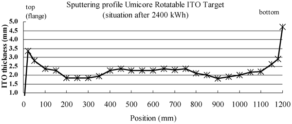
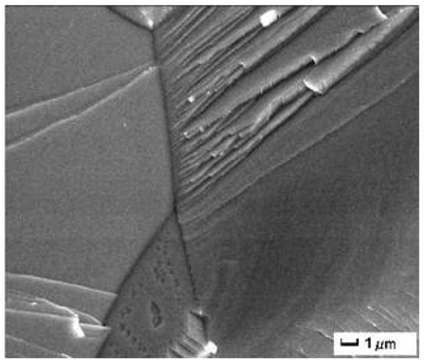
Erosion profile measured on rotary sputtering target surface after total sputtering energy of 2400 kW h
no abnormalities with plasma ignition at a high power level (up to 12 kW m−1)
uniform and steady plasma behaviour
stable cycling performance (e.g. stable sputtering voltage over a long period of time and low arcing)
sputtered nanostructured film with a high uniformity
practically no nodule and redeposition on the target.
The use of a rotary cathode allowed to apply a higher sputtering power. This possibility permitted to increase the deposition rate and, as a result, provided a higher efficiency of film deposition.
Conclusion
The developed and established technology of ITO ceramics using in-house prepared starting In2O3 powders allows manufacturing high quality and high density (up to 99·5% of TD) products with different dimensions and shapes. Ceramic components with areas up to 1750 cm2 for planar and rotary sputtering targets are commercially produced. Thanks to optimised compositions, high uniformity and densification, the manufactured ceramics possess low electrical resistivity and acceptable structural and thermal properties. As a result, nanosized ITO films with nanocrystalline or amorphous structures obtained by dc magnetron sputtering with fine tuned process parameters reveal low specific electrical resistivity and high transmittance required for applications in industrial large area and laboratory optoelectronic manufacturing. The use of rotary sputtering targets provides a significant increase in ITO film processing efficiency, greater utilisation of expensive ITO ceramics (up to 90%) and overall cost reduction with minimised nodule formation and redeposition during sputtering.
Footnotes
Acknowledgements
The assistance of Fraunhofer Institute for Thin Films and Surface Technology, FhG-IST Braunschweig (Germany), is greatly appreciated for the performance of XRD and high resolution SEM analysis of thin films.