
Abstract
Nanoscratch testing, as an important technique for the assessment of the mechanical failure behaviour and adhesion strength of ceramic coatings and a simulation tool of single asperity contact in tribological experiments, is increasingly becoming an established nanomechanical characterisation method. This paper reviews recent work in nanoscratch testing in different engineering applications including thin ceramic films, automotive organic coatings, chemical–mechanical polishing and biomaterials. In the main part of the paper, nanoscratch results from experiments performed using NanoTest systems fitted with tangential force sensors and spherical indenters as scratch probes are presented and discussed. The types of nanoscratch tests described include constant load nanoscratches, ramped load nanoscratch tests and multipass repetitive unidirectional constant load nanoscratch tests (nanowear). The results are discussed in terms of critical load sensitivity to intrinsic and extrinsic factors, impact of scan speed and loading rate, influence of probe radius and geometry, estimation of tip contact pressure, influence of surface roughness and film stress and thickness, and finally role of ploughing on friction evolution.
Introduction
Over the last 25 years, commercial nanomechanical testing instruments have expanded the range of their test techniques beyond simple nanoindentation to include capability for nanotribological measurements such as nanoscratch and nanowear testing, which has consequently greatly expanded their range of applications. Nanoscratch testing in particular is increasingly becoming an established nanomechanical characterisation method. It is mainly used for adhesion strength and mechanical failure modes measurement of ceramic coatings; however, it also brings interesting capabilities for nanoscale characterisation of bulk materials. Nanoscratch testing overcomes some of the limitations of atomic force microscopy (AFM) in terms of measurement stability and excessive tip wear on hard samples and is an important tool in simulation of single asperity contact in tribological experiments. It is a flexible method, which can be easily tailored to represent different application scenarios using various types of tip materials and geometries as well as different test kinetics with a constant or ramped applied load in a single or repetitive scratch mode.
In the design of coatings for improved tribological performance, a key issue to be resolved is the relationship between the coating mechanical properties and its adhesion to the substrate. It has been found that the mechanical response of a coated component is underpinned by the film/substrate system deformation behaviour rather than the adhesion strength alone.1–11 Both scratch resistance and interfacial toughness/adhesion under light and heavy loaded sliding contact can be assessed through nanoscratch experiments. Moreover, the progressive load nanoscratch test enables film performance throughout the load range to be assessed in a single test.
The majority of published work in nanoscratch testing area relates to establishing mechanical parameters of various coating/substrate systems. Roy et al. used nanoscratch test to characterise the interfacial adhesion of amorphous SiCN thin films deposited by plasma enhanced chemical vapour deposited (PECVD) method on Cu/Si substrates.12 The authors showed a relationship between the stresses in the coating and the cracking/buckling behaviour of the film observed experimentally, which was then further analysed by three-dimensional finite element model. A multilayer coating system Au/NiCr deposited on Al2O3 substrate was studied by Tang et al.13 Based on experiments, the coating deformation process was divided into three stages, and it was found that plastic deformation dominated over elastic deformation before the film failure for this metallic system. Various coating systems were investigated by Beake et al. by means of nanoscratch method.10,11,14–19 In the study of Beake et al.,11 high resolution scanning electron microscopy has been used in conjunction with progressive load nanoscratch testing and nanoindentation to investigate TiFeN, TiN and TiFeMoN film behaviour in highly loaded sliding and mechanical properties. It has been found that softer films exhibited lower ratios of hardness to modulus (H/Er), and films with H/Er≤0·11 possessed a more optimum combination of mechanical properties for applications where they are exposed to high shearing forces and strain in the film. In previous studies,14,17,19 much thinner (5, 20 and 80 nm) ta-C films deposited on Si (100) were assessed for potential applications in silicon based microsystems when mechanical contact occurs. Small scale fretting, nanoscratch and nanoindentation experiments were performed using spherical indenters to investigate the influence of the mechanical properties and phase transformation behaviour of the silicon substrate on tribological performance of films. A clear correlation between the fretting and nanoscratch tests was found despite the differences in contact pressure and failure mechanism.
Nanoscratch testing has been successfully used in other applications than coated systems. Noh et al. looked at the scratch characteristics of automotive organic coatings using nanoscratch tests.20 The results showed a close correlation between the scratch resistance data obtained from car wash experiments and nanoscratch tests and confirmed that mechanical properties, including scratch resistance, are improved with increased crosslinking networks in the coatings. In work carried out by Fu et al.,21 nanoscratch experiments were performed using AFM in deionised water and a slurry to investigate mechanical aspects of material removal process in chemical–mechanical polishing. Significantly deeper scratches were generated in slurry than in deionised water, which was attributed to a soft passivation layer generated during chemical interactions on the copper surface. Nanoscratch method has been also increasingly employed recently in biomaterials testing, where, among other cases, it was used to evaluate the wear behaviour of human root canal dentin,22 investigate tribological properties of polymethylmethacrylate based bone cements23 or compare mechanical behaviour of materials used in total hip replacement components.24
Although an international standard for nanoindentation now exists, nanoscratch testing is yet to be standardised despite being in increasingly common use. Project partners in the EU projects NANOINDENT25 and NANOINDENT-PLUS26 have been performing round robin investigations to deepen our understanding of the technique as a first step towards a test standard detailing the recommended experimental protocol and data interpretation in nanoscratch testing. In this paper, nanoscratch tests on coating and bulk materials using single pass constant and ramped loads method as well as multipass repetitive unidirectional constant load method are evaluated including studies on TiN films performed within the NANOINDENT project. The results are discussed in terms of critical load sensitivity to intrinsic and extrinsic factors, impact of scan speed and loading rate, influence of probe radius and geometry, estimation of tip contact pressure, influence of surface roughness and film stress and thickness and finally role of ploughing on friction evolution.
Experimental
The nanoscratch tests described include constant load nanoscratches, ramped load nanoscratch tests and multipass repetitive unidirectional constant load nanoscratch tests (nanowear). The progressive load nanoscratch tests were performed as a topography progressive load scratch topography multipass procedure. The progressive load ‘three-scan’ scratch tests, constant load single scratches and repetitive scratch tests (nanowear) were all performed using NanoTest systems (manufactured by Micro Materials, Wrexham, UK) fitted with tangential force sensors and spherical indenters as scratch probes. The end radii of the scratch probes were calibrated by nanoindentation. The design of the NanoTest combines high frictional sensitivity with sufficiently high lateral stiffness for accurate friction determination. Data were corrected in the NanoTest software to allow estimation of mean contact pressure by an in situ method without recourse to post-test imaging of scratch tracks. Table 1 summarises the systems studied and the scratch probe radii used.
Probe radius and film thickness in nano-scratch test studies
Results and discussion
Critical load sensitivity to intrinsic and extrinsic factors
Steinmann and coworkers reported that the critical load in the macroscale scratch test could be influenced by a range of extrinsic and intrinsic factors with intrinsic factors including scratching speed, loading rate and tip radius and extrinsic factors such as substrate hardness, and the roughness, thickness and friction of the coating.5 More recently, it has been shown that in addition to these factors, the mechanical properties of the coating also play a critical role in nanoscratch testing, with even quite small changes in H/E capable of altering the locus of film failure relative to the moving probe in hard nitride films.10,11 The lateral stiffness of the instrument is also important. If the test instrument can combine high frictional sensitivity with sufficiently high (i.e. optimised) lateral stiffness, then the probe traces remain very smooth until film failure. In contrast, if the instrument has insufficient lateral stiffness, the scratch tracks are wavy on all but the smoothest samples. A sensitive friction force capability in the nanoscratch test is highly desirable for several reasons including reliable quantitative friction data to be obtained, separate the interfacial and ploughing contributions to the total measured friction and clear identification of the onset of wear.
Scan speed and loading rate
The variation in critical load in the macroscale scratch test on a 3·5 μm thick CVD TiC coating on steel with a 200 μm radius diamond with scan speed and loading rate has been studied.5 It was found that for this system, the critical load decreased at lower loading rate and increased at lower scratching speed. However, provided tests were performed at a constant dL/dx ratio (the increase in load per unit scratch distance where L is the normal load and x is the scratch distance), the critical load was approximately constant within the precision of their measurements. Since a reduction in critical load was found when dL/dx decreases, it was recommended tests that be performed with a fixed dL/dx of 10 N mm−1. Steinmann et al. suggested that the probability of encountering defective adhesion within a certain load range increases when dL/dx decreases, resulting in a decreased critical load. However, this explanation may not apply for highly homogeneous coatings that do not fail by selective failure of poorly adhering regions and so exhibit very consistent Lc values, and also does not consider the possibility of cohesive failure.
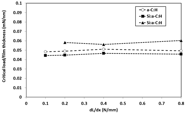
The influence of loading rate and scan speed on the critical load in the nanoscratch test has been investigated for diamond-like carbon (DLC) and Si doped DLC coatings on glass that show clear film failure.15 There was considerably less sensitivity to these scan parameters than has observed in macroscale scratch testing. When testing these samples at the nanoscale, no marked dependence on critical load was found on scratching speed, loading rate or (dL/dx) when dL/dx is much <1 N mm−1, while critical loads only slightly increase at higher dL/dx (1–5 N mm−1). Recently, Beake and coworkers have reported little clear variation in critical load for failure of an 80 nm ta-C film on Si over a 100-fold range of dL/dx.19 These results suggest that nanoscratch tests under significantly different loading conditions can be compared directly.
Topography progressive load scratch topography multipass scratch tests
An improvement on the basic nanoscratch test is the three-scan procedure (topography scan–progressive scratch–topography scan) that enables identification of failure mechanisms, the role of stress in particular, in more detail. The first reported multipass test of this type was described in detail by Wu and coworkers from IBM in 1989.27,28 In 2006, Beake and coworkers showed that by removal of the instrument compliance contribution to the measured deformation, the true nanoscratch and nanowear depth data could be displayed after levelling.10 By performing three-scan progressive load nanoscratch tests, it is possible to determine the critical load for the onset of non-elastic deformation since this is the load at which the residual scratch depth is no longer zero. The mean pressure at this point can be used as an estimate of the yield pressure.
Influence of probe radius and geometry
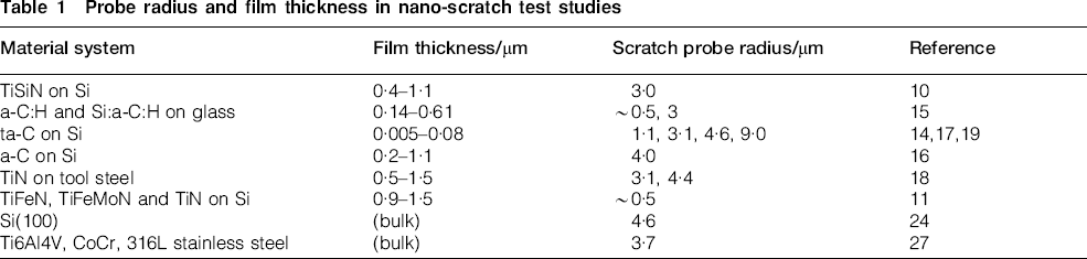
Material behaviour in the nanoscratch test is critically dependent on the radius of the test probe. Periodic calibration of the indenter radius by nanoindentation is necessary to determine the effective radius and ensure that the calibration remains accurate. If possible, this calibration should be performed with the probe in the same loading head. For bulk materials, transitions occur when critical pressures are reached, as in nanoindentation. The critical load at the onset of non-elastic deformation of fused silica appears to occur when a critical pressure of ∼8 GPa is reached. Assuming constant mean pressure (for a bulk material displaying no indentation size effects) leads to power law dependence with exponent of two for the variation of the critical load with probe radius. For coatings, the behaviour may be more complex when failures occur not solely at a critical pressure but are also associated with exceeding a critical bending strain in the coating.
Spheroconical probes with end radius typically 1–10 μm are commonly used in nanoscratch testing. Figure 1 shows the variation in the critical load for the total film failure of an 80 nm FCVA ta-C film on Si wafer. The critical load follows a power law dependence on the probe radius of the type shown in equation (1), where a is a measure of the effective adhesion strength in the nanoscratch test. The best fit curve to the data in Fig. 1 is given by a curve of y = 8·4x1·76.

Influence of probe radius on critical load for total film failure of 80 nm ta-C films on Si
The use of the spherical indenters has the additional advantage that the contact pressure analysis described below can be directly applied to the nanoscratch data, provided the instrument software has the capability to remove the contribution of instrument compliance, sample slope and roughness from the measured deformation data so that true nanoscratch and nanowear depth data are displayed.
Contact pressure
The progressive load multipass scratch technique has been improved by an analytical approach, which obtains accurate scratch depth data after correction of the raw data for the contribution from instrument compliance, sample topography and sample slope.
9
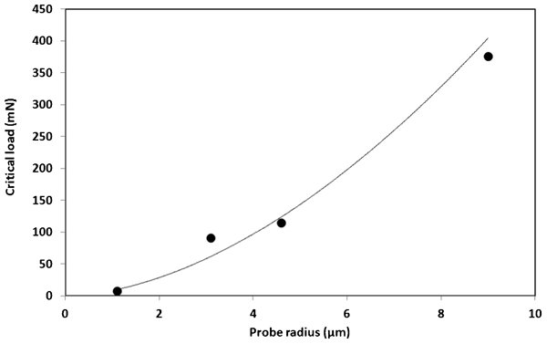
9,17 The method described by Beake et al.17 enables the yield stresses and the pressure required for the failure of the film to be estimated from contact mechanics, assuming the geometry of indentation, provided spherical indenters are used. Using spherical probes, the contact depth hp in an indentation contact is given by


the presence of a tangential load does not influence the pressure distribution too greatly so that the measured friction coefficient is well below 0·3
the radius of the indenter is constant
the sliding speed is sufficiently slow and contact sufficiently close to elastic that the load is supported on the rear of the indenter
the indenter can reach the bottom of the scratch track in the final topographic scan.
These conditions can be met in the nanoscratch test, although the approximation becomes less valid as the geometry moves away from Hertzian conditions due to increasing friction or plasticity. The methodology has been validated for thin films on silicon wafers with good agreement between scratch hardness independently determined from optical measurements of scratch widths and contact pressures for film and substrate yield events. The approach described above can also provide an estimate of the contact pressure during the progressive load nanoscratch test, at least at low contact forces where the friction coefficient is sufficiently low. It can provide an estimate of the mean contact pressure required to produce plastic deformation.
Nanoscratch testing has been applied to the study of the durability of metallic alloys (Ti6Al4V, CoCr and 316L stainless steel) that are increasingly popular for biomedical and other advanced applications.29 In order to develop improved mechanistic understanding for reliable artificial joint design, it is necessary to investigate the mechanical and tribological properties of biomedical materials at the relevant contact scale as these properties can be highly size dependent. Hardness and yield stress increase as the length scale of the contact is reduced (‘smaller is stronger’).30–32 Reported macroscopic yield stresses of these biomedical materials are in the range of 0·3–1 GPa, with stainless steel being lowest and Ti6Al4V being highest.33–35 Mean pressures for measurable plastic deformation in the nanoscratch test (defined by the first point in the final topographic scan showing non-zero depth) were ∼2·3 GPa for Ti6Al4V, ∼2 GPa for CoCr and ∼1 GPa for the 316L stainless steel. This ranking correlates with
 , which is a measure of the resistance to plastic deformation, and the reported macroscale yield stresses. The nanoscratch data show higher yield stress at the nanoscale, emphasising the importance of testing at the relevant scale rather than using bulk values.
Surface roughness
Beake and co-workers have recently investigated the influence of coating thickness, roughness and the direction of scratching relative to grinding marks on the behaviour of TiN coatings on M42 steel in single and multipass nanoscratch (nanowear) tests.18 TiN coatings (500 and 1500 nm) were deposited on M42 steel as this is a model system displaying clear failure with comparative frictional data available from previous macroscale scratch testing. The critical load for delamination failure was dependent on coating thickness and scratch orientation relative to polishing marks on the surface made before coating deposition. The critical load was 22% lower when scratching perpendicular to the grinding marks than parallel to them. Coating failure was more gradual when the scratch direction was either parallel to or aligned at an intermediate angle to the grinding grooves than when it was perpendicular. The dependence of the critical load on the direction of the nanoscratch orientation relative to the grinding marks is in agreement with literature results1 in scratch testing of thicker TiN coated high speed steel (HSS) with 200 μm probes. The decrease in critical load of ∼20–25% between scratches made across or parallel to grinding grooves for a TiN film with Ra = 0·12 μm in the nanoscratch test is similar to the macroscale result reported by Larsson et al. who found that below Ra = 0·1 μm, there was little influence of scan direction, but the critical load decreased by >50% when Ra reaches 0·5 μm.1 High roughness tends to decrease the critical load but the load carrying capability of higher thickness can have a much greater effect. Despite being much smoother, the critical load on 500 nm TiN was only ∼50% of the critical load on the 1500 nm TiN.
Influence of film stress and thickness
Coatings for mechanical property evaluation by nanoindentation have often been deposited on silicon as a readily available and smooth choice of substrate. Unsurprisingly, to date, many reports of nanoscratch testing have also involved thin coatings deposited on Si substrate. This has the advantage that coatings tend to be smoother but potentially adds some complexity since it has been shown that the combined response of the coating–substrate system can be strongly influenced by the contact induced phase transformation of the Si substrate. The nanomechanical and nanotribological characterisation of thin films on Si has involved nanoindentation with Berkovich indenters in combination with nanoscratch testing with spherical indenters.10,11,14,16,17,19 A key motivation was to understand the interplay between film thickness and interfacial toughness for microelectromechanical systems (MEMS) and other protective thin film applications. The reliability of Si based MEMS devices is limited by stiction forces when contact occurs. Applying very thin, low surface energy and low stress coatings can alleviate this problem, but it is critical that they are deposited optimally.
The film thickness is a key parameter influencing the critical load in the nanoscratch test. In principle, film thickness can have two opposing effects: thicker films that are harder than the underlying substrate provide more load support and so delay the onset of the substrate deformation that is often the precursor of film failure (higher critical load) and thicker films can be more highly stressed and more easily through thickness crack and delaminate when deformed (lower critical load) since the driving force for spallation to reduce stored elastic energy is greater.
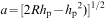
The relationship between film thickness and critical load can be quite complex in practice. Figure 2 shows how the critical load for film failure varies with the thickness of 5–80 nm FCVA ta-C films on Si when scratched by an R = 3·1 μm probe. The maximum von Mises stress is in the substrate at the critical load. It is deformation of the Si substrate by plasticity and phase transformation that drives the film failure. The increasing critical load with film thickness is due to the ability of the thin films to protect the Si substrate. Nanoscratch studies on 200–1000 nm a-C films deposited on Si by closed field unbalanced magnetron sputtering16 and 150–600 nm Si:a-C:H films deposited on glass by PECVD15 have shown that the critical load for total film failure in the nanoscratch test can be strongly correlated with film thickness reflecting enhanced load support and substrate protection.
Variation in critical load for total failure of 5–80 nm ta-C films on Si with their thickness
Provided the films are not too stressed, the ratio Lc/tf can be approximately constant in practice. Si doping during deposition resulted in small mechanical changes of DLC coatings of different thickness on glass, but the H/E ratio of the films remained approximately constant. After normalising the critical load by their thickness, as in Fig. 3, the films have similar scratch behaviour.
Critical load normalised by film thickness for 141 nm DLC and 366 and 614 nm Si doped DLC films on glass
As part of the NANOINDENT project, DLC films were deposited at BAM by CVD on Si to 450 and 962 nm thickness without an adhesion promoting interlayer.25 Nanoscratch testing with a 3·7 μm probe showed that both films delaminate easily, with the thicker film failing at only half of the critical load of the thinner film to due high stress. Substrate bias during deposition can significantly alter film stress. Shi and coworkers reported nanoscratch data for 200 and 1000 nm a-C films deposited with varying substrate bias voltage (−20 to −140 V) by closed field unbalanced magnetron sputtering.16 At 200 nm thickness, the highest H/E films performed best since the intrinsic stress in the film was relatively low (no recovery spallation and low H/E). For ∼1 μm a-C films, they observed a general relationship between H/E and the scratch test critical loads. When H/Er is ∼0·09–0·1, there was a tendency of the films to delaminate behind the moving probe at low critical load. Beake and coworkers previously reported a similar correlation for ∼0·8 μm Ti–Si–N nanocomposites films on Si.10 Higher H/E led to higher critical loads for elastic–plastic transition and also for the total film failure occurring in front of the probe. However, when H/Er was >0·09, film failure was always by tensile failure behind the probe (also described as unloading failure). The high tensile stress behind the probe in the nanoscale scratch test can lead to complete failure for hard films on silicon.
Beake and coworkers recently reported a similar correlation between the mechanical properties of hard 0·9–1·5 μm nitride based films on Si.11 At low scratching loads, the mechanical properties of the film itself control nanoscratch behaviour and films with higher H/E and lower plasticity indices are more resistant. At higher scratching load, the failure of harder films with H/Er>0·11 was accompanied by delamination outside the scratch track. It is suggested that hard films with H/Er≤0·11 possess a more optimum combination of hardness and toughness for applications where they will be exposed to high shearing forces and strain in the film in this case is more readily relieved by intergrain cracking.
The results of all these studies show the same trends. For optimum durability in highly loaded sliding contact, when films are deposited to ∼1 μm thickness, they should not be designed to be as hard and have as high a ratio H/Er as possible. For high H/E films, energy dissipation by mechanisms such as plastic deformation or localised intergranular fracture is less likely during the highly loaded sliding of these hard and elastic films, and ultimately, the stored elastic energy is instead relieved by dramatic fracture resulting in a larger delaminated area.11
Repetitive nanowear
More information can be provided by nanowear tests. Constant load, unidirectional multipass scratch testing was first described by Bull and Rickerby7 and has been shown to be an effective low cycle fatigue test. The same approach can be applied to micro- and nanoscratch testing. Constant load nanowear tests are often used to determine rates of sliding/abrasive wear and investigate the role of fatigue. A typical multipass experimental design is shown in Fig. 4. The low cycle nanowear experiments can often be much more informative regarding the influence of thin film stress, leading to poor adhesion than single scratch tests. When compared to progressive load nanoscratch testing, nanowear testing has the advantage that the load can be varied to tune the maximum von Mises stress to be close to the coating/substrate interface.
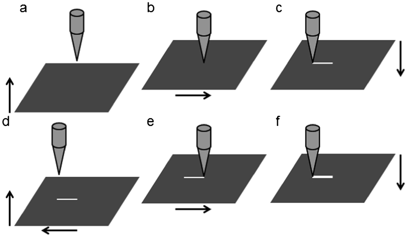
Schematic representation of first two cycles in unidirectional nanowear test:
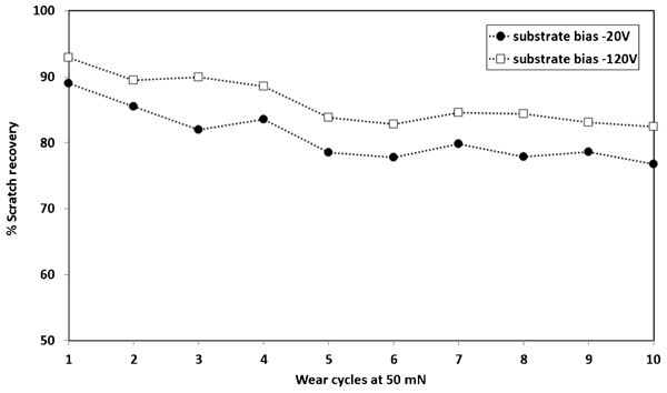
Evolution of scratch recovery and mean pressure during nanowear test on a-C films at 50 mN using 4 μm probe
Shi and coworkers performed subcritical load nanowear testing at two load levels to investigate the performance of 1 μm a-C films described above that fail in the progressive load nanoscratch test at a critical load of ∼200 mN.16 The wear test loads were chosen so that the maximum stresses were either within the film (at 50 mN) or the substrate (at 150 mN) so that the additional stress due to the imposed stress field from the scratch reaches the interface for the higher load test. In the lower load wear test, the contact is almost completely elastic with residual wear depths under 100 nm. Higher H/E films showed lower residual depth. An increase in residual wear depth and decrease in scratch recovery with each wear cycle (as illustrated in Fig. 5) confirm that the low load multipass wear test is a fatigue process.
For the film deposited at −20 V substrate bias (H/Er = 0·076), the mean pressure decreases from 9·0 GPa in cycle 1 to 7·9 GPa after 10 cycles. For the film deposited at −120 V substrate bias (H/Er = 0·089), the mean pressure decreases from 13·4 GPa in cycle 1 to 10·6 GPa after 10 cycles.
A reduction in contact pressure through the wear test has also been reported on hardmetals,37 biomedical alloys27 and TiN films.18 On 0·5 μm TiN, 10 cycles at 100 mN with a 4·4 μm diamond probe caused a decrease in contact pressure from 14·1 to 9·7 GPa, and the same conditions on 1·5 μm TiN led to a reduction from 15·8 to 11 GPa. Gee and Nimishakavi reported that a contact pressure of ∼8 GPa decreased to under 1 GPa within 10 cycles of a 20 μm diamond probe at 41·4 mN with contact pressure estimated from measurements of scratch width, which dramatically increases.
In marked contrast, when the subcritical load is a much higher fraction of the critical load, the behaviour is very different. Nanowear under these conditions is a very low cycle fatigue test where plasticity and microfracture dominate and the harder films deposited under high bias perform poorly. The behaviour of 1 μm a-C films with a very high ratio of H/E, deposited under high substrate bias, was found to be very strongly dependent on the test conditions, with the films performing well at low load wear but very poorly in more highly loaded contact.16 They exhibit low critical loads in progressive load scratch tests, and when they fail in the nanowear test, there is extensive delamination outside of the scratch track. The combination of nanowear tests at different loading levels provides information regarding the suitability of the a-C films for contact applications.
Friction evolution: Role of ploughing
The friction force in the nanoscratch test can be deconvoluted into its interfacial and ploughing components so that the interfacial friction can be reported (equation (5))

performing constant load friction test at very low force where contact is completely elastic and the ploughing contribution is zero
performing repetitive scratches to eliminate the ploughing contribution
performing progressive load scratch and extrapolating the low load friction data to zero load.
Typically, the friction coefficient at yield is of the order of 0·05.
Although frictional measurements are often reported to differ at different length scales, it appears that when the extent of deformation is taken into account, there is much better agreement. Friction force measurements on TiN in nanoscratch tests are in good agreement with conventional macroscale scratch testing with a 200 μm diamond probe. Dryda and Sayer reported 0·05 for a range of different 3–5 μm TiN coatings.38 The values of 0·04 (500 nm TiN) and 0·05 (1500 nm TiN) at 1 mN (R = 3·1 μm) appear to be good estimates for the interfacial component of the sliding friction. As the ploughing contribution increases, the total friction increases. The friction coefficient at film failure in the nanoscratch test is ∼0·2, consistent with macroscale determinations of 0·17–0·25.1,6,38
When friction and surface roughness are low, the loading curves in indentation and scratch tests can be surprisingly similar.24 As an illustration of this, Fig. 6 shows the response of Si(100) to indentation and scratch testing with the same spherical probe. The friction coefficient at pop-in is low (∼0·07), similar to the value of (0·08±0·01) that marks the onset of ploughing in nanoscratching with a 1 μm tip.39
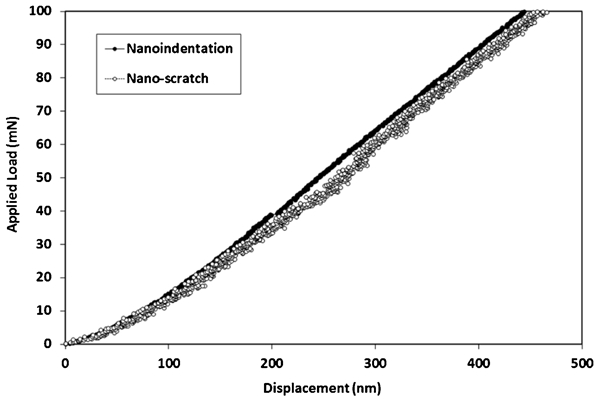
Typical load versus depth curves in nanoindentation and nanoscratch tests on Si(100) with 4·6 μm spherical probe
In contrast, metallic alloys such as 316L stainless steel and Ti6Al4V show a predominantly ductile response to scratching with ploughing and pile-up and debris at the sides of the scratch track, with the onset of chipping events at increasing applied load. Compared to Si(100), the metallic samples have higher friction at comparable load, and consequently, the deformation during the nanoscratch test is greater than in nanoindentation. The friction, wear depth and mean pressure evolve continually with repetitive scratching of metallic samples.
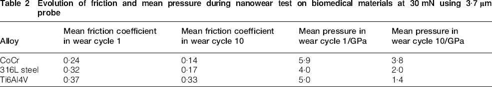
In the nanowear test, the Hertzian treatment is approximate on these alloys due to their high friction, but it can provide a convenient way to estimate contact pressures without the need for post-test imaging and can therefore be used to follow the evolution of contact pressure with repetitive scratching as has been performed in Table 2. The contact pressure decreases rapidly due to wear within a few cycles.27 The increase in the on-load probe depth over the 10 cycle wear test is ∼750 nm on the Ti6Al4V but only 100 nm on the CoCr. The Ti6Al4V alloy, which wears the most, consequently shows the largest drop in mean pressure.
Evolution of friction and mean pressure during nanowear test on biomedical materials at 30 mN using 3·7 μm probe
The observed frictional behaviour on repetitive sliding is explained by changes to the ploughing component of friction and smoothing of asperities, both of which alter the contact area and therefore can influence the friction.40 The evolution of friction and wear in the repetitive nanoscratch test can be followed by the parameters μ1/μn and d1/dn. For these metals, μ1/μn scales with d1/dn so that decreasing ploughing contribution results in μ (Ti6Al4V)>μ (316L stainless steel)>μ (CoCr). Studies of the relative importance of yield stress and microstructure on the evolution of friction and wear of metallic materials during microscale repetitive sliding have concluded that yield stress plays the dominant role on the evolution of friction as the friction was almost independent of the grain size but decreased with increasing hardness.41,42 On titanium, high friction (μ, ∼0·4–0·6) was observed virtually independent of grain size. With repetitive scratch testing, titanium showed little42 or no41 decrease in friction coefficient, and in the nanoscratch test, the decrease in friction was much less on Ti6Al4V than on either CoCr or 316L stainless steel. This is explained by a lower scan on scan decrease in the ploughing contribution on pure Ti and the Ti alloy. H/E can prove a more reliable parameter than hardness in predicting the sliding wear resistance of coated systems.43 For the biomedical alloys, it correlates with the extent of scratch recovery and the elastic recovery in nanoindentation. In the repetitive nanoscratches, it appears that both mechanical and interfacial properties can influence the wear behaviour. With continued scratch passes, the samples with lower hardness and higher friction, i.e. titanium alloy and stainless steel, show higher and more variable wear than the CoCr alloy. The different evolution in friction and wear on stainless steel, CoCr and TiAl4V may be related to differences in their stacking fault energies. The titanium alloy has a much higher stacking fault energy than either CoCr or stainless steel and does not work harden to the same degree, resulting in little reduction in ploughing and friction on repetitive nanoscratching.
In the nanowear testing of thin films, the friction force can be very sensitive to the onset of failure, unless the failure occurs behind the moving probe. Figure 7 shows the evolution of the friction coefficient with wear cycles at 100–300 mN for 1500 nm TiN on M42 steel being scratched with a 4·4 μm diamond probe. With repeat scratching, the friction coefficient initially decreases due to a reduction in the ploughing component as described above for metallic samples. The onset of coating failure was marked by a sudden sharp increase in friction during a single wear cycle, which is accompanied by an inflexion in the depth versus wear cycle. After the abrupt increase in friction at film failure, the friction decreases with continued scratch cycles as failure debris is removed from the scratch track.
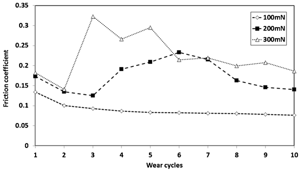
Variation in friction with number of wear cycles
Conclusion
In this paper, a review of recent progress in nanoscratch testing was carried out and the following conclusions can be drawn.
The critical load in nanoscratch test can be influenced by extrinsic and intrinsic factors. In addition, the mechanical properties of the coating and lateral stiffness of the instrument can also play an important role in nanoscratch experiments.
It has been observed that there was considerably less sensitivity to scan speed and loading rate in nanoscratch experiments than in macroscale scratch testing. The results suggest also that nanoscratch tests under significantly different loading conditions can be compared directly.
The nanoscratch three-scan procedure involving a sequence of topography scan, progressive scratch scan and topography scan enables identification of failure mechanisms and the role of stress in tested materials. Using this method, it is also possible to determine the critical load for the onset of non-elastic deformation.
Investigation of influence of probe radius and geometry revealed that periodic calibration of the indenter radius by nanoindentation is necessary to determine the effective radius and ensure that the calibration remains accurate. It has been also established that ∼5 μm represents an effective choice of end probe radius, ensuring that coating failure is observed within the force range of several commercial instruments but without risking rapid blunting of the indenter due to repeat scanning.
An approach based on indentation data enabling estimation of the contact pressure required for the failure of the film has been discussed. The approach can be used in the nanoscratch test, although it becomes less valid as the geometry moves away from Hertzian conditions due to increasing friction or plasticity.
Impact of surface roughness on nanoscratch experiments has been discussed and it has been shown that the critical load for delamination failure was dependent on scratch orientation relative to polishing marks on the surface made before coating deposition. Coating failure was more gradual when the scratch direction was either parallel to or aligned at an intermediate angle to the grinding grooves than when it was perpendicular.
It has been shown that the film thickness is a key parameter influencing the critical load in the nanoscratch test; however, the relationship between film thickness and critical load can be quite complex in practice. For optimum durability in highly loaded sliding contact, when films are deposited to ∼1 μm thickness, they should not be designed to be as hard and have as high a ratio H/Er as possible.
When compared to progressive load nanoscratch testing, repetitive nanowear testing has the advantage that the load can be varied to tune the maximum von Mises stress to be close to the coating/substrate interface. Nanowear experiments can also be much more informative regarding the influence of thin film stress leading to poor adhesion than single scratch tests.
The friction force in the nanoscratch test can be deconvoluted into its interfacial and ploughing components. It has been shown, however, that the impact of ploughing on friction has a complex mechanism and depends strongly on mechanical properties of tested materials.
Footnotes
Acknowledgements
We would like to acknowledge the contribution from our many collaborators and colleagues in the continuing development of the understanding of the nanoscratch test technique, in particular Drs J. Smith, M. Davies and S. Goodes of Micro Materials Ltd, Dr V. Vishnyakov and Professor J. Colligon of Manchester Metropolitan University and Dr B. Shi and Professor J. Sullivan of Aston University. The NANOINDENT project ‘Creating and disseminating novel nanomechanical characterisation techniques and Standards’ has received funding from the European Community's Seventh Framework Programme (FP7/2007-2013) under grant agreement no. NMP3-CA-2008-218659.FP7. The NANOINDENT-PLUS project ‘Standardising the nano-scratch test’ has received funding from the European Community's Seventh Framework Programme (FP7/2007-2013) under grant agreement no. NMP-2012-CSA-6-319208.