
Abstract
Microporous and macro-mesoporous silicon templates for surface-enhanced Raman scattering (SERS) substrates were produced by anodization of low doped p-type silicon wafers. By immersion plating in AgNO3, the templates were covered with silver metallic film consisting of different silver nanostructures. Scanning electron microscopy (SEM) micrographs of these SERS substrates showed diverse morphology with significant difference in an average size and size distribution of silver nanoparticles. Ultraviolet–visible–near-infrared (UV-Vis-NIR) reflection spectroscopy showed plasmonic absorption at 398 and 469 nm, which is in accordance with the SEM findings. The activity of the SERS substrates was tested using rhodamine 6G (R6G) dye molecules and 514.5 nm laser excitation. Contrary to the microporous silicon template, the SERS substrate prepared from macro-mesoporous silicon template showed significantly broader size distribution of irregular silver nanoparticles as well as localized surface plasmon resonance closer to excitation laser wavelength. Such silver morphology has high SERS sensitivity that enables ultralow concentration detection of R6G dye molecules up to 10−15 M. To our knowledge, this is the lowest concentration detected of R6G dye molecules on porous silicon-based SERS substrates, which might even indicate possible single molecule detection.
Keywords
INTRODUCTION
Surface-enhanced Raman scattering (SERS) spectroscopy is a highly sensitive technique widely used for identification and structural characterization of biological and chemical substances.1,2 It has retained all the advantages inherent to conventional Raman spectroscopy while overcoming its sensitivity drawback, which opens a wide range of new possibilities of the Raman technique for trace chemical analysis, environmental monitoring, and biomedical applications.3–5 The extremely high sensitivity is achieved by significant increase in the scattering cross section which can be several orders of magnitude higher than in conventional Raman spectroscopy. As a result, ultralow concentration detection can be attained, reaching even the ultimate limit of detection, single-molecule (SM) detection.6,7
The magnitude of SERS enhancement is highly dependent on the SERS-active substrate. 2 In past years, a large number of new SERS-active substrates were introduced due to the progress in nanoscience and nanotechnology. 8 They were produced by several methods, including electron-beam lithography, nanosphere lithography, and films over nanospheres.
In the past decade, noble-metal nanostructures deposited on porous silicon (pSi) templates have been extensively investigated as an easy-to-fabricate and cheap SERS substrate.9–12 Porous silicon is a nanostructured material obtained by anodization of crystalline silicon in hydrofluoric (HF) acid solutions. 13 Due to its large active surface area, which can be easily functionalized by different noble-metal nanostructures, this semiconductor material has become suitable for preparation of sensitive SERS substrates. Silver and sometimes gold are most commonly used for synthetizing nanoparticles often by the immersion plating method,9,14 but also the thermal decomposition method, 10 the method of anchoring colloidal nanoparticles, 15 and the inkjet printing method. 16
The morphology of the final SERS-active substrate obtained by the immersion plating method, and consequently, the enhancement of Raman signal of adsorbed molecules, depends on two main factors. The first is the underlying porous silicon structure, which in its turn, is determined by the type of silicon wafer used and the etching conditions.13,17 It is shown in the literature that the majority of authors use highly doped p- or n-type silicon wafers9,11,14,16,18–21 to produce mesoporous silicon templates for SERS substrates. However, a few of them reported utilization of low dropped silicon wafers15,22–24 for creation of macroporous silicon templates. The second factor that influences the morphology of SERS substrate is the deposition conditions, mainly the concentration of the metallic salt solution and the deposition duration.11,21
Here, we propose a simple technique for preparation of two types of SERS substrates by using micro- and macro-mesoporous silicon templates created from low-doped p-type silicon wafers. The production and characterization of microporous silicon were elaborated in more details in our previous paper. 25 The SERS substrate was thereafter prepared by immersion into silver nitrate (AgNO3) solution, which yielded a uniform layer of mostly spherical silver nanoparticles with narrow size distribution. In the second case, the macro-mesoporous silicon template was prepared by using additional treatment in hydrofluoric acid solution yielding macropores with mesoporous substructure. In this case, by the immersion plating method, much bigger silver nanoparticle aggregates with broad size distribution and irregular shapes with sharp edges were formed. The activity of both types of SERS substrates was tested using rhodamine 6G (R6G) dye molecules, evidencing detectable concentrations as low as 10−9 to 10−15 M. To our knowledge, this is the lowest concentration detected on pSi based SERS substrates, which might even indicate possible SM detection.
EXPERIMENTAL
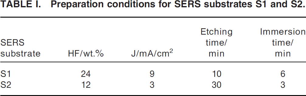
Micro- and macro-mesoporous silicon templates were produced by an anodization process from p-type, boron doped wafers with resistivity of ∼1 and ∼20 Ω·cm, respectively. The wafers (Prime Wafers Inc.) were cut into 4 cm2 squares and placed on the aluminum base of a Teflon etching cell using Ga-In as a back contact. The exposed surface of the silicon wafer electrode was 2.55 cm2, adjusted by an O-ring at the bottom of the cell. After etching, the templates were rinsed twice in ethanol and dried in air.
The pSi template for SERS substrate S1 was produced by etching ∼1 Ω·cm wafers in 24 wt.% HF acid ethanol solution for 10 min at constant 9 mA/cm2 current density, forming a highly luminescent homogenous microporous layer. The silver nanostructures were synthesized by immersing freshly prepared pSi template into 10−2 M AgNO3 aqueous solution. After 6 min (Table I), it was established by visual inspection of color changes of the surface that a uniform silver layer was produced. The pSi template for SERS substrate S2 was produced by etching ∼20 Ω·cm wafers in 12 wt.% HF acid ethanol solution for 30 min at constant 3 mA/cm2 current density, forming macroporous silicon overlaid with a highly luminescent microporous layer. To remove the luminescent microporous layer, the template was additionally immersed in 32 wt% HF acid-ethanol solution for 60 s, leaving the macroporous surface covered with mesoporous substructure. The silver nanostructures were synthesized by immersing a freshly prepared pSi template into 10−2 M AgNO3 aqueous solution for 3 min (Table I). Prepared SERS substrates were rinsed in redistilled water and dried in air.
Preparation conditions for SERS substrates S1 and S2.
To estimate the Raman activity, SERS substrates and pSi templates were cut into 3 × 3 mm2 squares and incubated for 2 h in 1 mL of R6G aqueous solutions. The R6G concentrations ranged from 10−2 to 10−15 M with 10−1 M step, giving a total of 14 samples per SERS substrate and pSi template, which were then dried in air.
Raman spectra were obtained by the Horiba Jobin Yvon T64000 triple Raman spectrometer in backscattering geometry. The samples were mounted under the microscope equipped with 50× long working distance objective (0.5 NA) and illuminated with 514.5 nm Ar+ laser excitation wavelength. The laser spot diameter was ∼0.8 μm, thus providing a scattering area of ∼0.5 μm2. The recording time was adjusted from 1 to 5 s with intensities from 10−8 to 10−6 W/μm2. The morphology of SERS substrates and pSi templates was obtained using a Jeol JSM-7000F thermal field emission scanning electron microscope (FE-SEM) operating at 5 and 15 kV accelerating voltage and the working distance of 10 mm. The plasmonic response of the nanostructured silver film deposited on substrates S1 and S2 was determined from the UV-Vis-NIR spectra using a Shimadzu spectrometer (model UV-3600) with the integrated sphere in total reflectance mode.
RESULTS AND DISCUSSION
The FE-SEM image of the pSi template for the S1 substrate shows a flat surface homogenously covered with numerous micropores (Fig. 1a). Such a microporous layer has random, nanometric spongelike structure with less than 2 nm pore size and fairly large surface area that can easily be accessed and chemically modified. On the other hand, the pSi template for the S2 substrate shows an uneven surface covered with numerous macropores of different depths and diameters between 1 and 3 μm (Fig. 1b). Higher magnification reveals a mesoporous substructure with pores 10–30 nm in size that completely covers the surface (Figs. 1c and 1d).
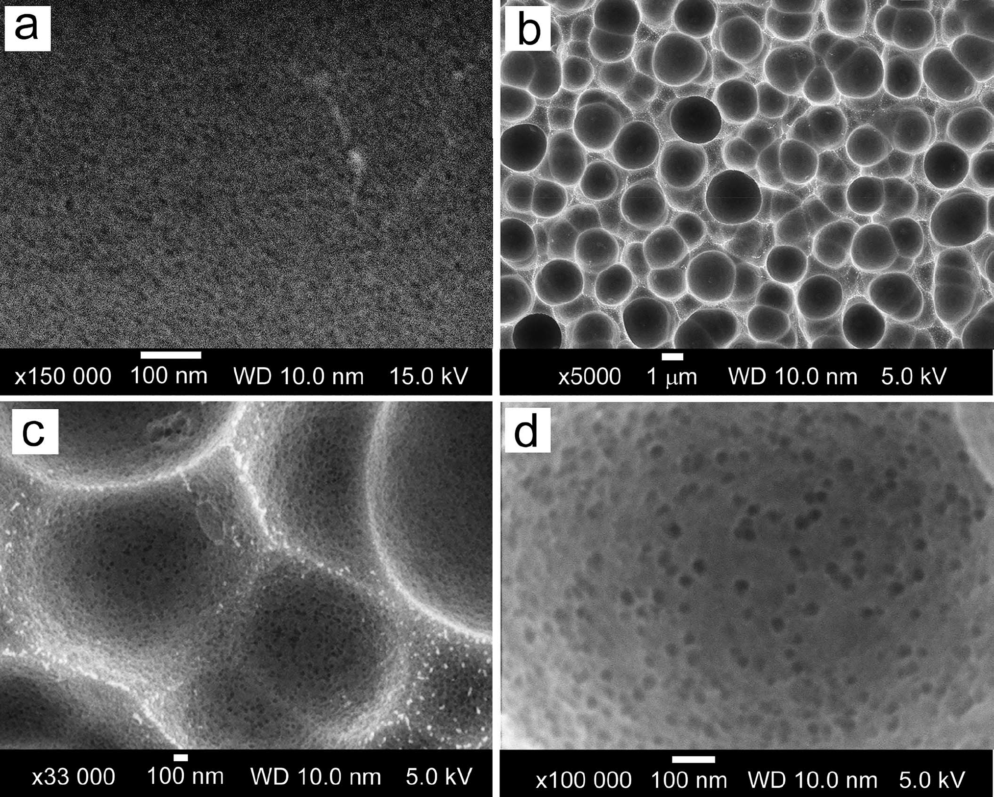
FE-SEM micrographs of pSi templates S1 and S2. (
According to the model proposed by Harraz et al., 27 the immersion of the pSi template into AgNO3 solution leads to spontaneous deposition of silver nanoparticles. During the immersion, the oxidation of the porous silicon surface and the reduction of silver ions occurs, which results in close-packed silver nanoparticles film. The morphology of the pSi surface provides a large density of appropriate sites for the nucleation and growth of silver nanostructures, and hence it has strong influence on the morphology of the deposited silver film. The FE-SEM micrograph of substrate S1 shows silver nanoparticles uniformly covering the surface (Fig. 2a). Higher magnification (Fig. 2b) reveals densely packed particles that are mostly spherical in shape while some of them have partially coalesced. The calculated size of the nanoparticles was 31 ± 13 nm with narrow size distribution as shown in Fig. 2c. This morphology suggests that the nucleation of silver nanoparticles started almost simultaneously at numerous sites across the whole microporous surface.
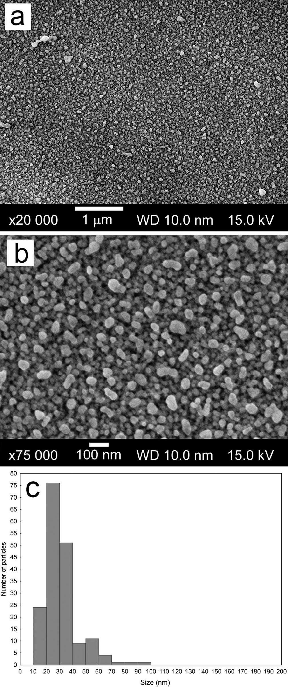
FE-SEM micrographs and distribution of silver nanoparticles of substrate S1. (
Contrary to that, the FE-SEM micrograph of substrate S2 shows good coverage of shallow macropores and pore walls, while the penetration of silver nanoparticles into the deep macropores could not be observed (Fig. 3a). A higher magnification micrograph (Fig. 3b) reveals the coalesced nanoparticles with highly irregular shapes and facetted forms with sharp edges. In between them, much smaller almost spherical particles are observed leaving interparticle distance sometimes less than 10 nm. The distribution of nanoparticles is relatively broad with calculated size of 65 ± 35 nm (Fig. 3c).
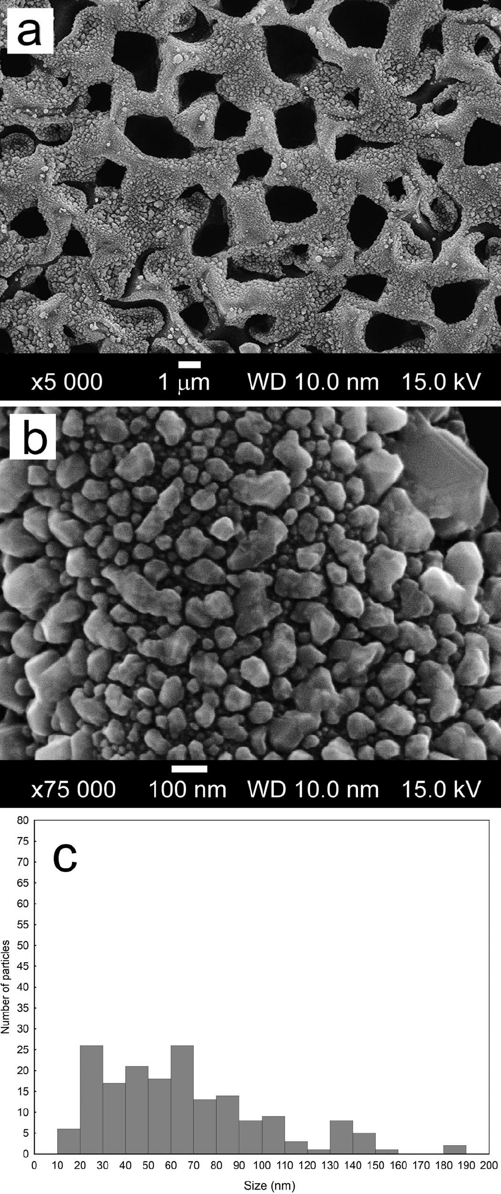
FE-SEM micrographs and distribution of silver nanoparticles of substrate S2. (
The optical response of metallic nanostructures is commonly measured by UV-Vis-NIR spectroscopy. In the case of non-transparent samples, such as in this experiment, the UV-Vis-NIR reflectance spectroscopy was used. Major spectral bands include the interband transitions of bulk silver around 320 nm and the broad LSPR band covering a majority of the visible spectral range (Fig. 4). 29 The position of the LSPR band of silver nanostructures depends on their structural properties, such as the size and the shape, as well as the interparticle gap spacing. 30 The increase of the nanoparticle size, the shape complexity, and the decrease in the interparticle distance shifts the LSPR band position towards the longer wavelengths.31–33 However, the width of the LSPR band mostly depends on the size distribution of particles.
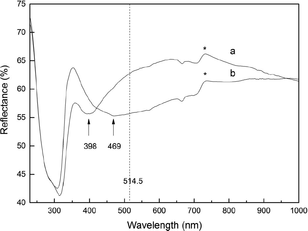
UV-Vis-NIR spectra recorded in total reflectance mode. The spectra (
Surface-enhanced Raman scattering substrates S1 and S2 exhibit different optical responses in the position and width of the LSPR band (Fig. 4). The LSPR band of substrate S1 is much narrower in comparison to substrate S2, which has a broad width as if it was composed of several bands. In addition, the difference in the LSPR band peak positons for 72 nm was observed. Substrate S1 contains particles with a narrow size distribution (Fig. 2c) and an almost regular spherical shape (Fig. 2b); hence, as it is expected, its LSPR band is narrow. Contrary to that, substrate S2 contains two times larger particles with broad size distribution (Fig. 3c), which redshifts and broadens the LSPR band. Additional contribution to the shift and width of the LSPR band could also be due to the irregular shapes of nanoparticles, as well as the nanoparticle interactions as a result of small gaps between them, sometimes less than 10 nm.
The Raman activity of SERS substrates and pSi templates was tested with R6G probe molecules which are well characterized in SERS spectroscopy. 35 The R6G molecules were randomly adsorbed throughout the surfaces of the samples by immersing them into R6G aqueous solutions at different concentrations ranging from 10−2 to 10−15 M with a 10−1 M step. The Raman spectra were recorded with the excitation laser wavelength of 514.5 nm, which is close to the absorption maximum of R6G (around 532 nm), indicating that resonant conditions were achieved. The R6G molecules have extremely high fluorescence quantum yield, and in a case of resonant excitation, one would expect a strong fluorescence. When the Raman spectra were recorded from R6G molecules adsorbed on pSi templates, the florescence background overwhelmed the Raman signal. Hence, the lowest detectible Raman signal was achieved for 10−3 M concentration, but when R6G molecules were close to the nanostructured silver surface, such as on SERS substrates, their fluorescence was quenched to a large extent by rapid energy transfer from the excited electronic state to the silver surface. Along with that, the Raman signal was enhanced due to SERS effect, and hence, the achieved detection limit of R6G molecules was 10−6 and 10−7 M for S1 and S2, respectively. At concentrations below those, only broad background spectrum, common in SERS measurements for all types of silver substrates, was present. The recorded spectrum had two broad bands, one around 1365 cm−1 and the other around 1585 cm−1, which are characteristic for disordered carbon materials. 36 That background was present even if the Raman spectrum was recorded from the SERS substrate only and was ascribed by Lin et al. 9 to the adsorption of contaminants during the preparation and storage of SERS substrates.
It is established that, at low concentrations, the R6G molecules are heterogeneously distributed throughout the sample, 18 and hence, it is very likely that they will be missed if the random place is taken to record the Raman signal. Therefore, in order to obtain the SERS spectrum, a large number of random sites were probed by manually scanning the samples under the microscope and recoding the Raman spectra with 1 s integration time. By this method, the detection limit was much improved, being 10−9 and 10−15 M for the S1 and S2 substrates, respectively (Fig. 5). Surface-enhanced Raman scattering spectra show prominent R6G vibrational bands at 1363, 1509, 1575, and 1651 cm−1, which correspond to C-C aromatic stretching vibrations. 35 In addition, at ultralow concentration (10−15 M), the background with bands around 1365 and 1585 cm−1 is visible.
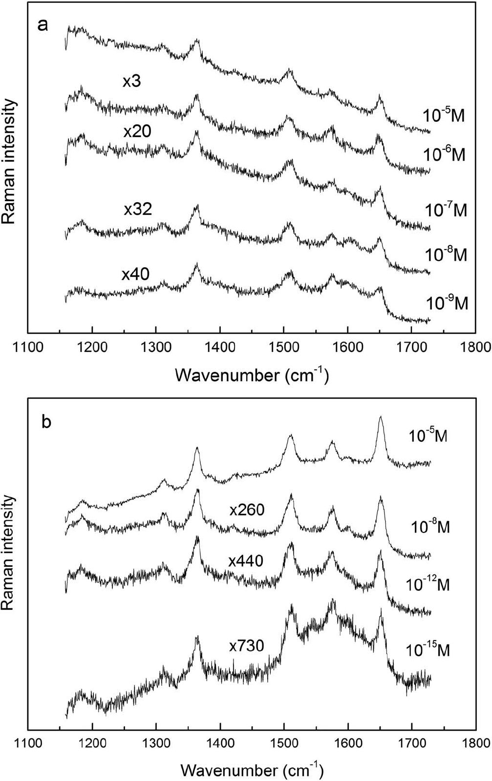
The SERS spectra of R6G molecules for substrates: (
To estimate the performance of SERS substrates, the enhancement factor 37 is usually calculated. Since the morphology of prepared substrates is quite complex, the reliable estimation of the number of molecules producing the signal is questionable. Hence, we used another parameter of merit called the external amplified Raman efficiency (EARE), which was proposed by Virga et al. 19 It is defined as the ratio of minimum detectable concentration of probe molecules obtained on the pSi template to the one obtained on the SERS substrate. For substrates S1 and S2, the calculated EAREs were 10 6 and 10 12 , respectively. The reason for this difference in substrate performance could have two origins. First, the electromagnetic theory 38 of SERS predicts the maximal signal enhancement when the laser excitation is tuned to the absorption maximum of localized surface plasmons, i.e., the LSPR band minimum in the reflectance spectra. In this experiment, the laser excitation wavelength was closer to the LSPR band minimum for substrate S2 (Fig. 4), which explains its better performance. Second, the additional contribution to average signal enhancement is due to the presence of so-called “hot spots”. Those are the gaps between two or more closely spaced interacting metallic particles 39 or particles with sharp nanoscaled corners and edges 40 where large enhancement of the EM field is present. Since both SERS substrates were silver metallic films with random roughness and densely packed nanoparticles, it was expected that both of them have hot spots, but the morphology of substrate S2 (Fig. 3b) exhibited coalesced nanoparticles with highly irregular shapes and facetted forms with sharp edges that indicate a higher probability of hot spot formation. This could additionally improve the substrate's performance and lead to a lower concentration detection limit.
Additional indication that more hot spots are present in substrate S2 than in substrate S1 was obtained by monitoring the change in the integral intensity of the R6G Raman band at 1363 cm−1 with concentration (Fig. 6). A recorded Raman spectrum at each concentration was normalized with the respect to the recoding time and laser power used in the experiment and baseline corrected prior to calculating the integral intensity. As was expected, with the decrease of R6G concentration, the Raman integral intensity was also decreasing for both substrates up to the concentration 10−6 M for S1 and 10−7 M for S2. For lower concentration, as previously mentioned, the surface coverage with R6G molecules of both substrates was incomplete and uneven, and hence, a large number of random sites had to be probed in order to obtain SERS spectra. Figure 6a shows that, by doing so, the integral intensity of the R6G Raman band at 1363 cm−1 decreases for substrate S1 up to the concentration of 10−9 M. For lower concentrations, the Raman spectrum could not be obtained, even though the thorough probing of random sites was performed. For substrate S2 (Fig. 6b), the integral intensity was continuously decreasing up to the concentration of 10−11 M. Below this concentration, very few R6G molecules are expected to be inside a laser spot diameter, and hence, to record a good Raman signal, they should be situated near the hot spots. The inset of Fig. 6b shows that, at concentrations below 10−11 M, the integral intensity of the 1363 cm−1 band is nearly independent on R6G concentration. At those ultralow concentrations, the position of the R6G molecules against hot spots and the activity of hot spots have crucial influence on the intensity of the SERS signal. Since the detection limit for substrate S1 was 10−9 M, while for substrate S2, it was 10−15 M, it was assumed that substrate S2 had much more hot spots with the right morphology to produce large enhancements, and hence, the probability of detecting R6G molecules is much higher.
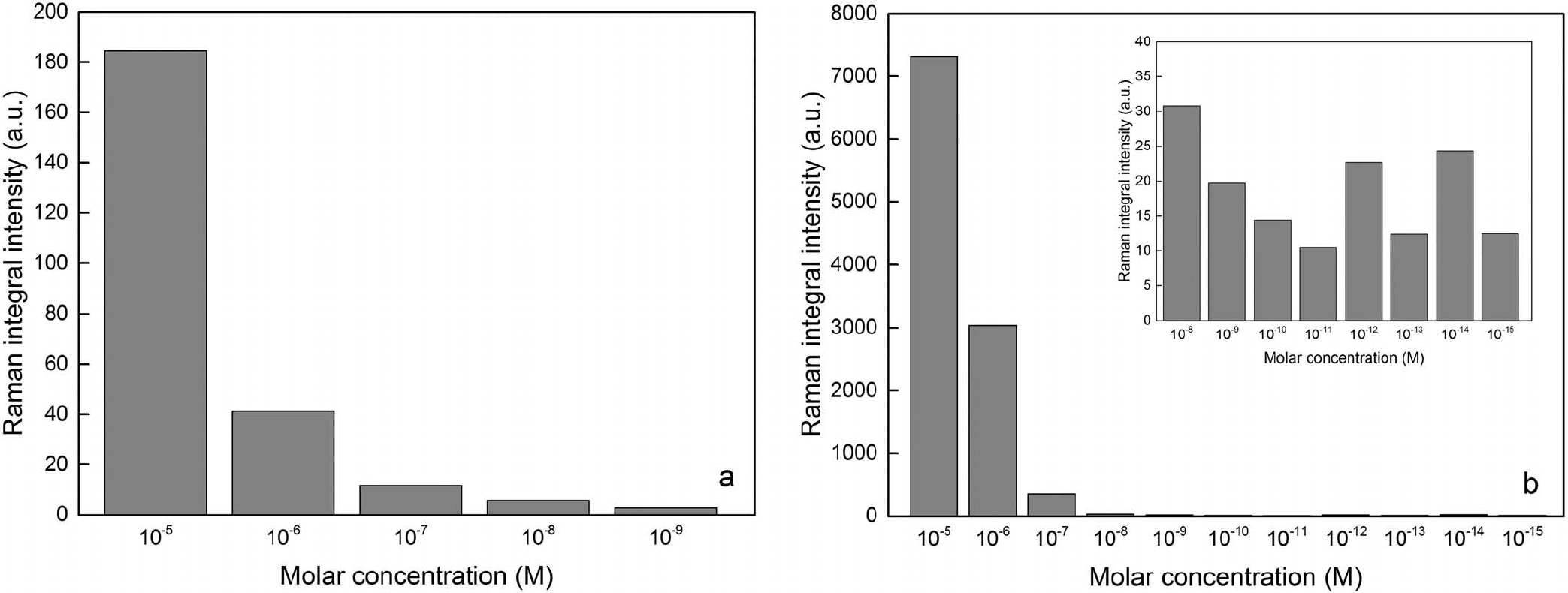
The integral intensity of Raman vibrational band at 1363 cm−1 vs. different R6G concentrations for substrates (
Recording the Raman signal at such high dilutions raises the question whether SM detection is plausible. According to Pieczonka and Aroca, 41 SM detection is possible on the silver metallic films where hot spots are realized with analytes that provide resonant Raman conditions. Taking into account that this experiment was done with highly diluted R6G concentrations in resonant conditions on the substrate containing highly active hot spots, it is plausible to assume that the Raman signal is likely to originate from one or several molecules. However, to confirm SM detection on these substrates, another more reliable approach should be used, such as the bi-analyte method 42 or the techniques of Langmuir-Blodgett films. 43
CONCLUSION
In this paper, we have proposed a simple technique for preparation of pSi templates from which highly sensitive SERS-active substrates were produced. By electrochemical etching of low doped p-type silicon wafers, a microporous silicon template was obtained, while additional immersion into HF acid solution produced a macroporous template with mesoporous substructure. Silver nanoparticles were deposited by the immersion plating method, yielding a uniform layer of mostly spherical silver nanostructures on a microporous template and much bigger silver aggregates with irregular shapes and sharp edges on a macro-mesoporous template. The activity of SERS substrates was tested using R6G dye molecules in resonant conditions. We confirmed better SERS performance of the substrate formed from a macro/mesoporous template whose silver film morphology was heterogeneous with broad distribution of sizes and shapes, which induced a lot of highly effective hot spots. In addition, the peak of the LSPR band for this substrate was closer to the excitation laser wavelength, which altogether enabled ultralow concentration detection of R6G molecules down to 10−15 M. To our knowledge, this is the lowest concentration detected on pSi-based SERS substrates, which might even indicate possible SM detection. Since porous silicon is characterized by easy and inexpensive fabrication of nanostructured silver films, it has great potential in the SERS field.
Footnotes
ACKNOWLEDGMENTS
The authors acknowledge the Croatian Science Foundation (Project “Hybrid Silicon Nanostructures for Sensing”) and the University of Zagreb (Project BM1.18) for the financial support of this investigation.