
Abstract
A huge number of parabens, esters of p-hydroxybenzoic acid, are used in cosmetic and personal care products as preservative substances. Due to their detrimental effects on ecosystem and human health, taking precautionary measures to remove these compounds is an important task regarding the environmental issues. In this study, a silica (SiO2) nanotube has been selected as a novel sensor to adsorb the most common parabens which are methyl paraben and propyl paraben molecules. To this aim, density functional theory (DFT) calculations were used to evaluate the properties for investigated compounds. The calculated adsorption energies of the most stable configurations for methyl parban@SiO2 and propyl paraben@SiO2 complexes were found to be –0.238 and –0.242 eV, respectively. The electronic properties of nanotubes experienced dramatic changes in case of interactions with parabens, which led to declining the HOMO/LUMO energy gap of the nanotube to its original value. Such adsorption could also enhance the electrical conductivity of the nanotubes meaning that the utilized SiO2 nanotube could detect the existence of methyl and propyl parabens molecules in the environment. As a concluding remark, the investigated SiO2 nanotube could work as a possible sensor for hazardous paraben with the importance of environmental issues.
Introduction
Parabens are esters of parahydroxybenzoic acid, which mainly include methyl paraben (MP), ethyl paraben (EP), propyl paraben (PP), butylparaben (BuP), and benzyl paraben (BP) [1]. It is almost a century that single standing parabens or in combination with other compounds, have been routinely utilized as preservatives in formulation of approximately all types of cosmetics, pharmaceuticals, and food products because of having antibacterial and antifungal effects [2, 3]. Furthermore, the widespread use of parabens as the most common preserving agents is attributed to their extraordinary physical and chemical properties such as having imperceptible odor or taste, chemical stability at high temperatures or wide pH range, low toxicity, and low production cost [4]. Earlier research works have shown a direct correlation which exists between increasing the anti-microbial activity of parabens and the chain length of their aster group; however, the shorter esters including MP and PP are frequently used because of their higher solubility in water [5–8]. Over the past few years, the vast use of paraben compounds has raised worldwide concerns about their unpredictable influence on human life and environment systems [9]. Although paraben safety has been proven by various studies, currently, some in vitro studies have identified parabens as Endocrine-Active Chemicals (EACs) which might make an adverse impact on human health [10]. Since parabens are able to be adsorbed by skin, their estrogenic activity may increase the risk of breast cancer or the male reproductive tract [11, 12]. In order to remove these hazardous compounds, a number of techniques have been applied such as extraction of parabens from cosmetic products and environmental samples using Solid Phase Extraction (SPE), Gas Chromatography–Mass Spectrometry (GC–MS), and adsorption has been reported [13–15]. Among them, the adsorption techniques have been considered as cost-effective and practical ways to remove and detect specific compounds [16]. This task is very much important regarding the environmental issues especially for the industrial societies.
Silica (SiO2) nanotube, discovered by Nakamura et al. in 1995, have drawn a great deal of attention because of their exceptional properties such as hydrophilic nature, easy colloidal suspension formation, and distinctive inner and outer surfaces [17]. In addition, their widespread applications in many fields including separation, adsorption, catalysis, optics, electronics, drug delivery, and chemical sensing have led to remarkable advances in the use of silica nanotubes in medicine and industry [18–20]. Since the discovery of SiO2 nanotube, a wide range of research on their preparation and the application has been carried out such as utilizing the SiO2 nanotube as the catalyst carriers by Zhang et al. [21] and introducing it as adsorbents for heavy metals by Wang et al. [22] It is important to note that after pioneering discovery of carbon nanotube (CNT), considerable efforts have been dedicated to characterize features of this novel material and its relatives [23–26]. Moreover, non-carbon and other types of nanostructures have been invented and introduced for different purposes [27–30]. Si-O bonds could provide more reactive surface for SiO2 nanotube regarding the electronegativity difference ∼1.5 between each of Si and O atoms in comparison with identical carbon atom composition of CNT [31]. Therefore, the idea of investigating its application for adsorption purposes could be interesting due to existence of such reactive tubular surface. In this case, computational works did dominant roles to detect and characterize such important characteristic features for nanostructures to reveal insightful information for researchers of specific fields of studies and applications [32–36].
Regarding the importance of paraben removal by nano structures, [15] interactions of MP and PP with SiO2 nanotube have been investigated in this work by the computer-based quantum chemical computations at the molecular scale. Structural geometries and electronic features were evaluated to reach the aim of this work to probably introduce SiO2 nanotube as an adsorbent for hazardous paraben counterpart (Table 1 and Figs. 1–6).
The adsorption energy (EAds) of MP and PP molecules on SiO2 nanotube, and energy fermi (EFermi), the charge on the molecule after its adsorption (QT) on the nanotube, the HOMO-LUMO energy gaps (EG) and the change of nanotube HOMO-LUMO gap upon the adsorption processes and Percentage Sensitivity of the compounds (% S)
The adsorption energy (EAds) of MP and PP molecules on SiO2 nanotube, and energy fermi (EFermi), the charge on the molecule after its adsorption (QT) on the nanotube, the HOMO-LUMO energy gaps (EG) and the change of nanotube HOMO-LUMO gap upon the adsorption processes and Percentage Sensitivity of the compounds (% S)
aThe change of EG of nanotube upon the adsorption process.
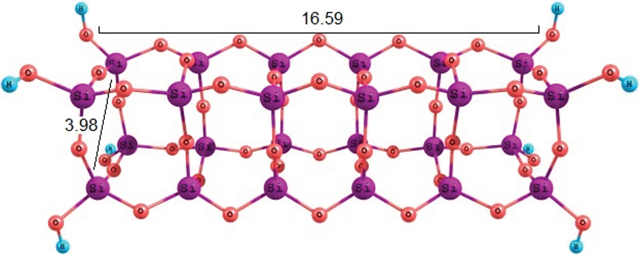
The optimized structure of original SiO2 nanotube.
Within this work, a representative single-wall SiO2 nanotube consisting of 24 Si and 52 O atoms was investigated as possible adsorbent for paraben molecules (Fig. 1). Avoiding the dangling effects, the ending atoms of nanotube were terminated by additional hydrogen atoms [37–39]. Geometries of original SiO2 nanotube were optimized at the B3LYP/6-31G* level of density functional theory (DFT) to reach the minimized energy structure. Moreover, singular molecules of paraben (EP and PP) were optimized at the same theoretical level of computations. Subsequently, interactions between each of paraben molecules with the SiO2 nanotube were examined at the mentioned theoretical level of computations including dispersion correction [40]. Moreover, the basis set superposition error (BSSE) was examined for the interacting complex systems showing almost negligible errors to energy values [41]. After energy calculations and optimization processes, electronic properties such as Molecular Electrostatic Potential (MEP), Natural Bonding Orbital (NBO), and Density of States (DOS) were evaluated for the investigated systems. All results of this work were obtained by the GAMESS program [42] and they were included in Table 1 and Figs. 1–6 fo further discussion on the topic.
Results and discussion
Optimized structure of SiO2 nanotube
The optimized structure of original SiO2 nanotube was shown in Fig. 1. After optimization process, the length and diameter of nanotube were calculated to be about 16.59 and 3.98 Å, respectively. Moreover, the length of Si-O bonds of optimized SiO2 nanotube were calculated in two types of Si-O bonds; one with the bond length of 1.63 Å lying in the octagonal rings, and another one with the bond length of 1.65 Å related to atoms bridge the rings (Fig. 2). These results were in close agreement with the available bond lengths of Si-O reported by Qiao et al. [43]. The energy gap (EG) between the highest occupied and the lowest unoccupied molecular orbitals (HOMO and LUMO) for the mentioned configuration of nanotube was 8.03 eV (Table 1). In order to determine the minimum adsorption configurations of Paraben@nanotube, the MP and PP molecules were initially placed one by one at different positions above the considered SiO2 nanotube with different orientations, so various configurations were used for optimization to reach the best minimized energy structure.
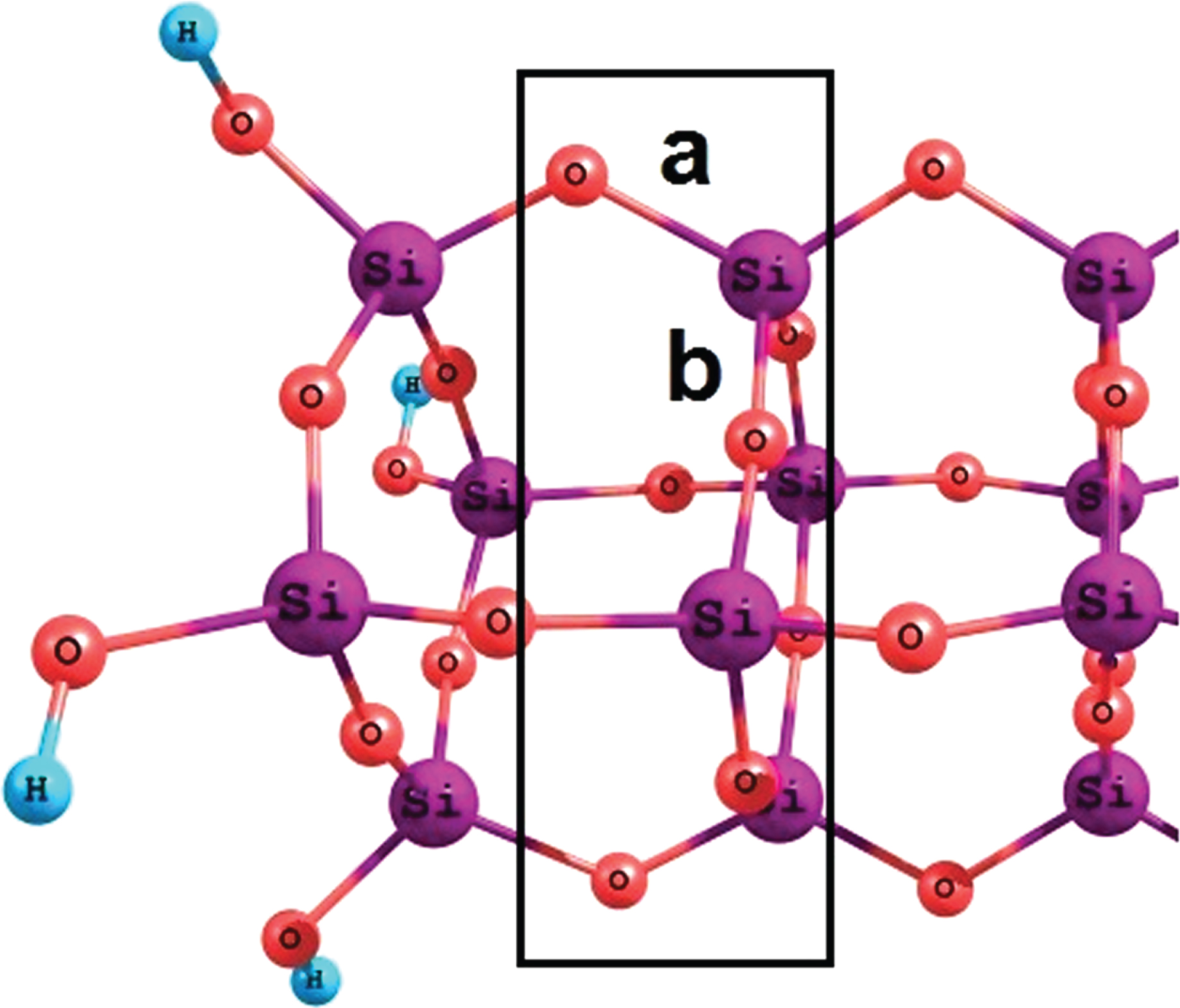
Two types of Si-O bond: a) Si-O bond that bridges the rings (1.65 Å), b) Another one lies in the octagonal rings (1.63 Å).
First, methyl paraben (MP) was selected for interacting with SiO2 nanotube to study the adsorption properties between adsorbate and adsorbent. Finally, after full structural relaxation, the most stable adsorbed configuration was achieved for the MP@SiO2 complex. The O atom of carbonyl group of MP oriented toward O atom of the octagonal ring with the distance of 2.86 Å (Fig. 3). This configuration was an exothermic process with negative EAds of –0.238eV and a charge transfer of 0.029 |e| from the molecule to the nanotube surface. These results indicated that this interaction could be accepted as chemisorption. The value of EG was calculated to be 5.24 eV for the MP@SiO2 complex. Detailed information including values of EAds, NBO charge transfer, EG, and ΔEG (change of EG of nanotube upon the adsorption process) ere all summarized in Table 1.
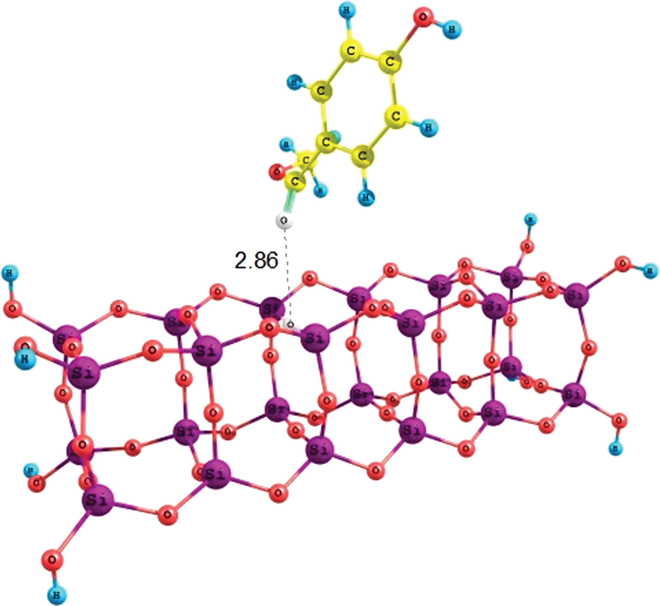
Optimized structure of stable MP@SiO2.
Likewise, to examine the sensitivity of the adsorption of SiO2 nanotube as an adsorbent for propyl paraben (PP), several adsorption configurations were applied by placing PP on various sites of the tube with different orientations. The most favorable configuration of PP@SiO2 complex was shown in Fig. 4. The calculations showed that PP adsorption was exothermic process with EAds of –0.242eV and distance from nanotube surface to PP was 2.92 Å, indicating that this interaction could be also chemisorption. In this configuration, a net charge of about 0.031|e| was transferred from the molecule to the nanotube surface. The value of EG of the PP@SiO2NT complex was calculated to be about 5.36 eV (Table 1).
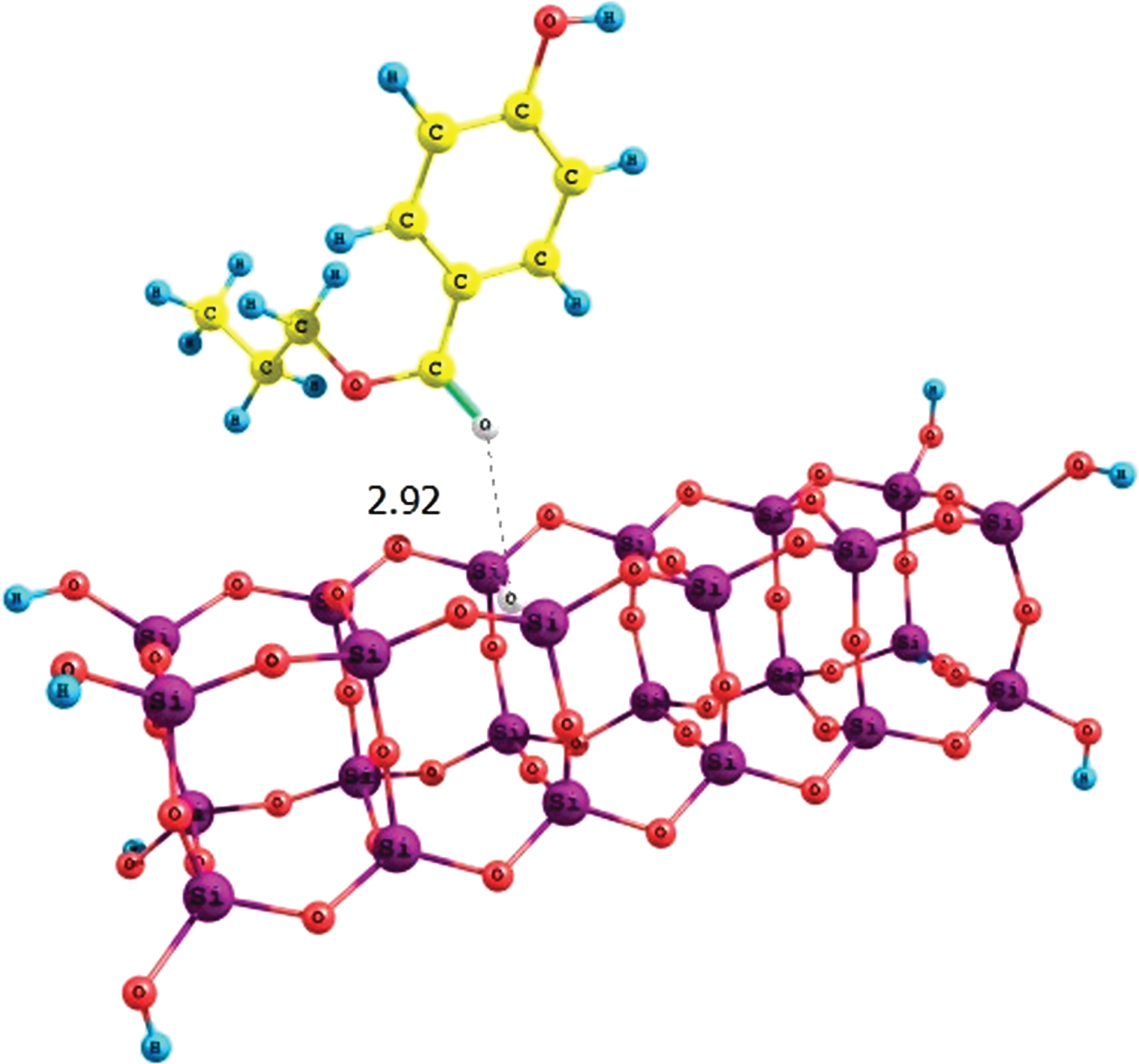
Optimized structure of stable PP@SiO2.
The charge distribution explained by molecular electrostatic potential (MEP) surface analysis gave us a deeper insight into MP@SiO2 and PP@SiO2 adsorption processes. In this regard, MP and PP cases were selected for MEP computations on the SiO2 nanotube surface. MEP is the molecular electronic potential surface generated by the charge distribution of the molecule, which could be defined at the atomic sites using eq. (1).
ZA is the charge on nucleus A, located at RA. The sign of V(r) depends on whether the effects of the nuclei or the electrons are dominant at any point. The MEP has repeatedly been used for investigation of the chemical properties of several materials [44–46]. As shown in Fig. 5, MEP plots in the most stable configurations indicated that Si atoms were blue representing positively charged atoms while the O atoms were located in red color area due to being negatively charged in Si-O bonds of tube surface. This implied that there were ionic bonds in the nanotubes surface, caused by charge transfer from O atoms to the Si ones. MEP analysis done on the most stable state of MP@SiO2 and PP@SiO2 also elucidated that there was a reaction between oxygen atom of the tube and carbonyl oxygen of each adsorbate.
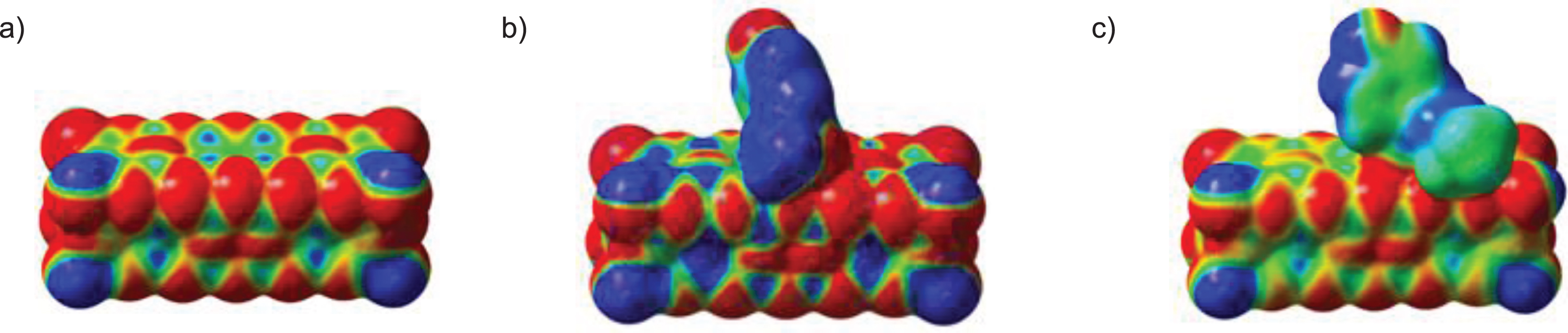
Calculated molecular electrostatic potential (MEP) surface for (a) original SiO2 nanotube, (b) MP@SiO2, (c) PP@SiO2. The surface is defined by the 0.0004 electrons/b3 contour of the electronic density. Color ranges in a.u.: blue is more positive than 0.050; red is more negative than –0.050.
The electronic properties of all structures were studied by DOS plots providing much more meaningful understanding of the nature of interaction. As shown in Fig. 6, Comparison of DOS plots demonstrated that the electronic properties of adsorbent after adsorption of MP and PP molecules were significantly altered, indicating a decline in the EG of adsorbent from 8.03 eV in free model to 5.24 and 5.36 eV, showing a considerable change of EG about 2.79 and 2.67 for MP@SiO2 and PP@SiO2 complexes, respectively. In the other words, after the adsorption process the value of EG decreased and therefore a substantial increase occurred in conductivity. This phenomenon could be explained by eq. (2) [47].
Where σ is the electrical conductivity and k is the Boltzman’s constant. According to eq. (2), the smaller EG at a room temperature leads to the higher electrical conductivity. Furthermore, it was observed from figures that there was a considerable reduction in Fermi level after each adsorption process as a result of transferring a huge number of electrons during the interaction between each adsorbate and SiO2 nanotube. Energy of Fermi level could be found by averaging values of HOMO and LUMO levels to show the medium state for electron transferring features. For the current investigated models, charge redistribution and electronic changes in the structure of the adsorption system significantly affected the electrical conductance of the materials. These results revealed that electronic properties of SiO2 nanotube were highly sensitive to the mentioned paraben molecules adsorption. Therefore, it seems that the SiO2 nanotube may be a practical sensor for the MP and PP molecules detection.
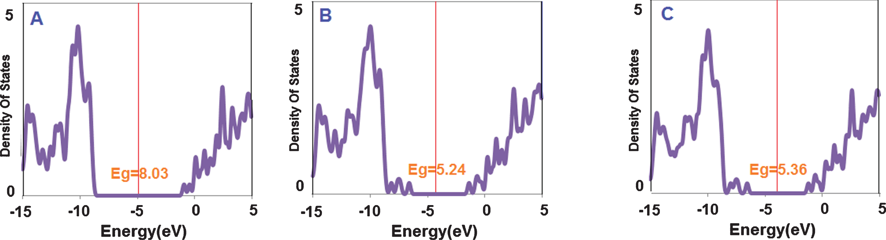
Density of state (DOS) plots for (a) original SiO2 nanotube, (b) MP@SiO2, (c) PP@SiO2.
In summary, the aim of this computational work was to investigate the adsorption of MP and PP on the surface of SiO2 nanotube using DFT calculations of structural and electronic properties including bond lengths, energy gaps, and adsorption energy. Calculations demonstrated that SiO2nanotube could perfectly adsorb MP and PP molecules on its surface through chemisorption mechanisms with notable adsorption energies. Beside, MEP and DOS analyses endorsed that during MP adsorption and then PP adsorption on the tube surface, a charge was transferred between adsorbate and adsorbent molecules. Due to this process, their HOMO/LUMO energy gap decreased about 2.79 and 2.67eV for MP@SiO2 and PP@SiO2 complexes, respectively, which altered the electronic properties of the nanotube. Hence, the electrical conductivity of SiO2 increased upon the adsorption processes. The results of this study clearly suggested that SiO2 could potentially be considered as a novel sensor for detection of MP and PP molecules and applied as a practical way to remove these unfavorable molecules from environment, especially in industrial societies.