
Abstract
Titanium nitride (TiN) films were generated in the abnormal glow discharge (AGD) region and the glow-arc transition discharge (GATD) region by varying target current density (Ja) in an Ar/N2 atmosphere in the pulsed DC magnetron sputtering system. The effects of different discharge regions on the structure and mechanical properties of TiN films were investigated by X-ray diffraction (XRD), scanning electron microscopy (SEM), scratch test and micro-hardness test. The results indicated that all TiN films exhibited a strong (220) preferred orientation. Ja of 0.24 A cm−2 was a demarcation point between the AGD and GATD region. Compared with the AGD films, the GATD TiN films exhibited smooth surface, regular dense columnar structures and small grain sizes. Especially, TiN films deposited at 0.4 A cm−2 showed the highest hardness (2388 HV) and the best adhesion (up to 55 N).
Keywords
Introduction
With the development of economy, science and technology, people have put forward higher requirements on the ability of various products to withstand the bad environment. In order to make the existing products run stably under the bad environment for a long time, the surface modified film of high hardness and wear resistance has become the first choice [1-4]. TiN films are widely used in today's industrial fields because of their advantages, such as high hardness, excellent wear resistance and corrosion resistance. At present, the main technologies for preparing TiN films are magnetron sputtering ion plating (MSIP) and arc ion plating (AIP) [5]. However, the discharge region of MSIP is the abnormal glow discharge (AGD) region. The particles produced by MSIP are mostly low-energy neutral atoms, which makes it difficult to form dense, well-bonded TiN films [6,7]. This disadvantage severely limits the application of TiN films in the precision manufacturing industry. Although the AIP particles exhibit high ionization rate and energy, the surface melting of the target is easy to produce micrometre-sized large particles in arc discharge region, which can reduce the quality of TiN films.
To know more about the influence of target current density (Ja) on plasma characteristics and mechanical properties of TiN films, we decided to further research the glow-arc transition discharge (GATD) region by varying Ja. In this article, the target surface temperature, structure, average deposition rate and mechanical properties of TiN films deposited in the AGD and GATD region had studied for comparison.
Experimental section
The deposition condition of TiN films.
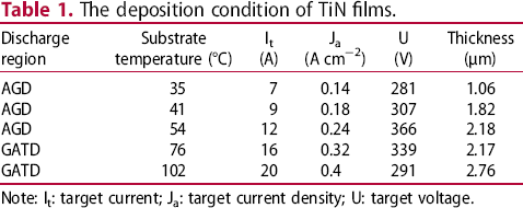
Note: It: target current; Ja: target current density; U: target voltage.
The Ti target surface temperature was measured by a Model WRP-130 thermocouple (SAIC Instruments, Maximum: 1300°C). The distance between the measuring point and the thermocouple was 10 mm. The crystal structure of TiN films was characterized by X-ray diffraction (XRD-7000s, Japan) with Cu-Kα anode (voltage: 40 kV, current: 40 mA). The surface morphology and cross section of films were characterized by field-emission scanning electron microscope (Merlin Compact-6170, Germany), and the thickness of the films was calculated by the cross section. The adhesion of TiN films deposited on HSS was evaluated by WS-2005 scratch test. The applied load was increased from 0.05 N up to 60 N in 1 min and the scratch length was 3 mm. The hardness values were tested by HVT-1000 digital micro-hardness test with a load of 50 gf and a holding time of 15 s.
Results and discussion
Physical parameters of the electrical discharge process
Figure 1 shows the target voltage (U) – current density (Ja) curve of the Ti target. When Ja increases from 0.14 to 0.4 A cm−2, the U first increases and then decreases, with an inflection point at 0.24 A cm−2. The reason of the U change is that the bombardment of high-energy argon ions causes the target surface temperature to rise due to the increase in Ja. When Ja gradually increases to 0.24 A cm−2, the target surface temperature rapidly attains the degree of thermionic emission due to the interaction of argon ions bombardment and Joule heating [7]. High flux of electrons, argon ions and Ti atoms increases the collision ionization rate, and the increase in ions and electrons leads to the improved conductivity. Thus, as Ja is >0.24 A cm−2, the U gradually decreases to 306 V.
The electrical discharge target voltage-target current density (Ja) curve of the Ti target (the pressure of 1.5 × 10⁻³ Torr in a purity Ar atmosphere).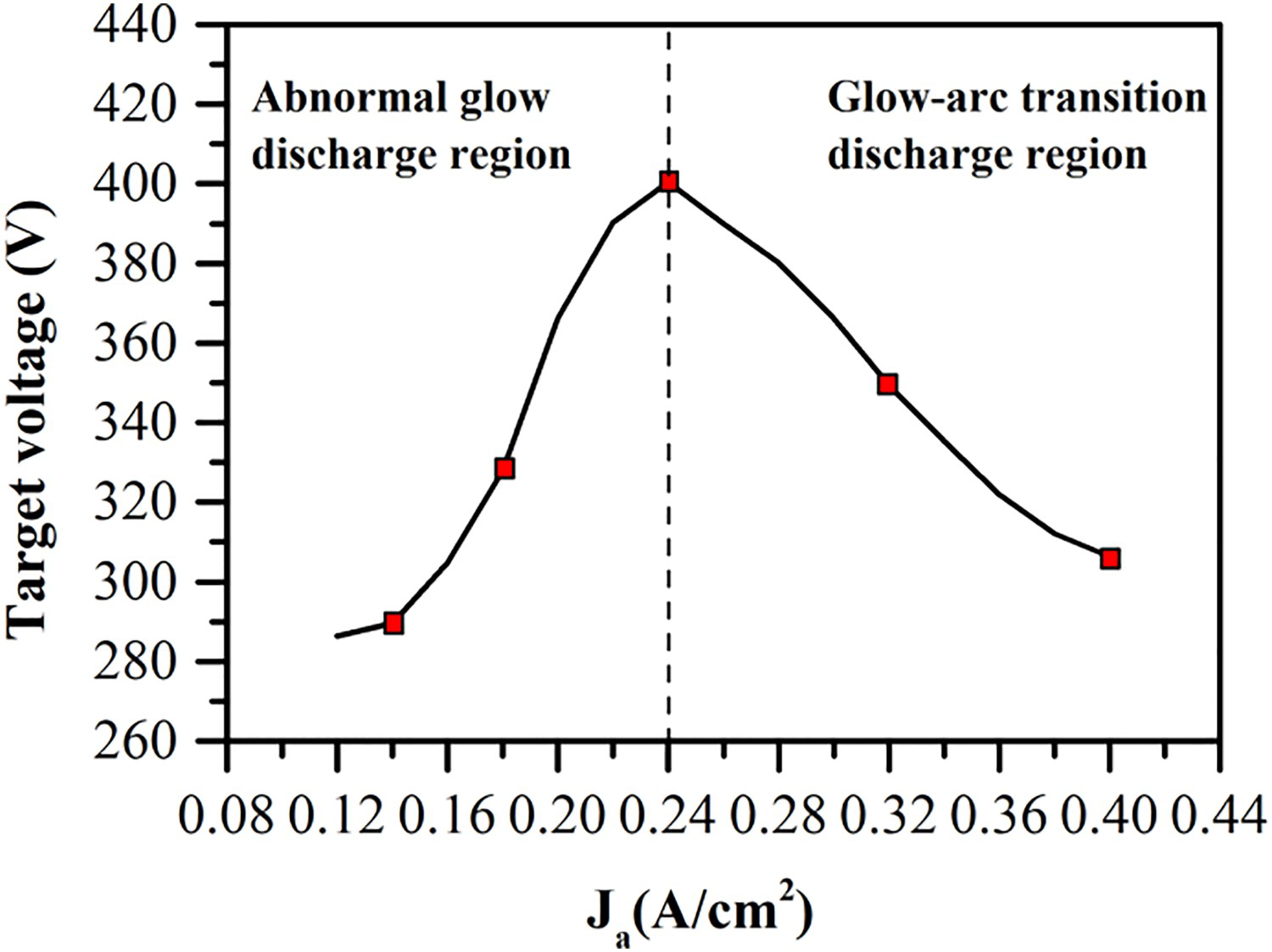
The Ti target surface temperatures at different Ja are 397, 602, 1013, >1300 and >1300°C, respectively. Edison effect [8] indicated that thermionic emission phenomenon of metals tended to be significant for temperatures over 1000°C. The Ti target surface produces high flux of heat emission electrons as Ja increases to 0.24 A cm−2 and the number of heat emission electrons increases rapidly with the increase in Ja from 0.32 to 0.4 A cm−2, which is consistent with the discussion in Figure 1.
Structure and average deposition rate of TiN films
Figure 2 displays the XRD patterns of TiN films deposited at different Ja. All TiN films exhibit a NaCl type face centre cubic (fcc) structure (JCPDS 38-1420). All TiN films exhibit a strong (220) preferred orientation. According to different reports [9,10], TiN films often grew toward the (111) or (200) orientation, because the films generally grew along the direction of reducing the total energy on the system. However, according to I. Iordanova et al. [11], the development of the TiN (220) plane can be attributed to high flux of particles bombarding the growing films. In this paper, Ja is higher than the normal magnetron sputtering current density range (<0.1 A cm−2). This is the reason why the (220) orientation appears. Figure 2 shows the weaker diffraction peak intensities of (111), (200) and (311) except for Ja at 0.32 A cm−2, which exhibits a mixture structure dominated by the (220) orientation. With the increase in Ja from 0.14 to 0.4 A cm−2, the (220) peak intensity first increases and then decreases. The transformation of (220) peak intensity is due to the effect of particle energy. The high energy and flux of the deposited particles promote the growth of the (220) crystal plane due to the increase in Ja. When Ja >0.32 A cm−2, the particles with excessive energy destroy the growth of the (220) peak. The average grain sizes of the films were estimated by the Scherrer formula [12-14], the grain size of TiN films increases from 63 nm to 96 nm as Ja is less than 0.24 A cm−2. However, as Ja continues to increase to 0.4 A cm−2, the average grain size decreases instead of increasing, which is 92 and 73 nm, respectively. The grain size of TiN films is mainly affected by deposition rate and substrate temperature [15]. In the GATD region, high deposition rate and low substrate temperature can form many nucleation sites and reduce the critical nucleation size, resulting in a smaller grain size.
XRD patterns of TiN films deposited with different Ja.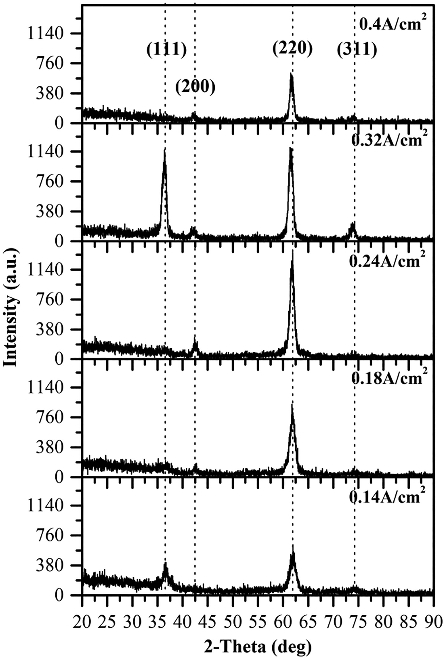
The top view SEM micrographs of TiN films deposited on single crystal silicon are presented in Figure 3. The top view micrographs of TiN films change from irregular shape granules (Figure 3(a)) to pyramidal granules (Figure 3(c)) as Ja increases from 0.14 to 0.24 A cm−2. The AGD TiN films exhibit many micropores on its surface. However, the increase in Ja to 0.4 A cm−2, it is evident that TiN films exhibit dense hilly granules (Figure 3(e)). In the GATD region, Ti particles exhibit high ionization and energy. Under high-energy ions bombardment, the diffusivity of particles is improved by transferring energy from ions to deposited particles on the substrate. In films growth stage, many nucleation sites can be formed, and a large number of nucleation sites and high-mobility can form a dense and smooth surface morphology, as shown in Figure 3(d,e).
Top view SEM micrographs of TiN films deposited with different Ja: (a) 0.14 A cm−2, (b) 0.18 A cm−2, (c) 0.24 A cm−2, (d) 0.32 A cm−2, (e) 0.4 A cm−2.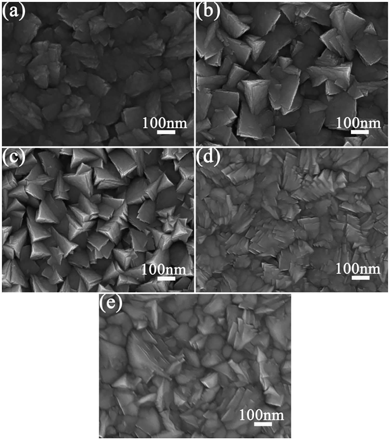
Figure 4 presents the cross-sectional SEM micrographs of TiN films. With the increase in Ja, the density of boundary pores between columnar grains increases gradually, as shown in Figure 4(a–c). Moreover, the growth of columnar grains in the AGD region is disordered. Compared with the micrographs (Figure 4(a–c)), it is evident that GATD TiN films exhibit regular dense columnar grains (Figure 4(d,e)), and the density of boundary pores significantly decreases as Ja increases to 0.4 A cm−2. This is because the energy and diffusion ability of the AGD particles are lower, and it is easy to form a porous columnar morphology [6]. However, the GATD particles exhibit high ionization rate, diffusion ability and energy. Owing to the faster deposition rate of GATD particles, a large number of nucleation sites are formed. Nucleation sites and high mobility can form regular dense columnar crystal structure, resulting in the dense structure of GATD TiN films.
Cross-sectional SEM micrographs of TiN films deposited with different Ja: (a) 0.14 A cm−2, (b) 0.18 A cm−2, (c) 0.24 A cm−2, (d) 0.32 A cm−2, (e) 0.4 A cm−2.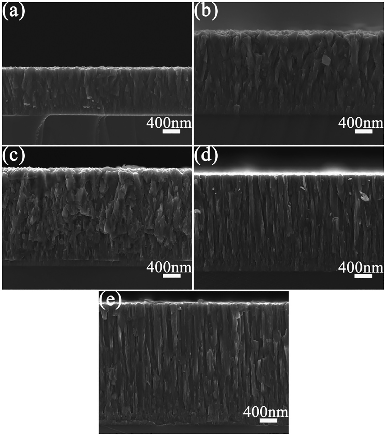
The average deposition rates of TiN films were determined by thickness measurements which were the average value of 5 positions per sample. The average deposition rate of TiN films deposited on Si is illustrated in Figure 5. The average deposition rate increases from 42.4 nm min−1 to 87.2 nm min−1 as Ja increases from 0.14 to 0.24 A cm−2, and it could be related to the increase in the U and the plasma density. Nevertheless, the average deposition rate is almost unchanged as Ja increases from 0.24 to 0.32 A cm−2. This can be attributed to the competition of the following two factors. On the one hand, the decrease in U in the GATD region reduces the energy of argon ions, which is likely to decrease the sputtering yield of Ti atoms. On the other hand, the increase in Ja enhances the density of the plasma, which is beneficial to improve the deposition rate. As Ja >0.32 A cm−2, a large number of electrons spontaneously escape from the Ti target surface and drag out high flux of Ti atoms. As a result, the average deposition rate of TiN film increases to 110.4 nm min−1.
The average deposition rate of TiN films with different Ja.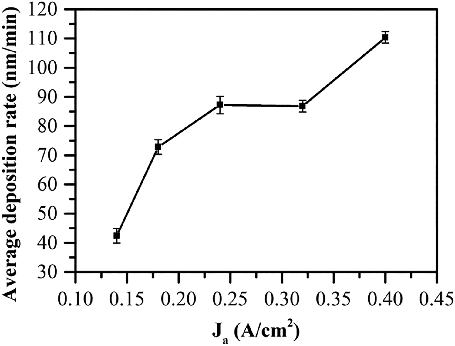
The above results exhibit that there is a strong correlation between the plasma properties generated in different Ja and the structure of TiN films. I. Petrov et al. [16] showed that varying the ratio of incident ions to neutral particles (Ji/Jn) during deposition could be a useful tool for controlling structure and properties of films. In fact, the intrinsic effect of varying the incident ion to neutral flux ratio is to vary the ionization rate of particles. In this paper, the variation of Ji/Jn ratio is indirectly characterized by the ratio of bias current to thickness of films (Ji/Jfilm). As Ja increases from 0.14 to 0.4 A cm−2, Ji/Jfilm is 0.23, 0.25, 0.28, 0.37 and 0.48, respectively. Ji/Jfilm of the AGD region varies from 0.23 to 0.28. However, the value of Ji/Jfilm increases rapidly from 0.37 to 0.48 as Ja increases in the GATD region. Owing to the bias current is positively correlated with the ions and electrons, it means that the ionization rate of particles in the GATD region is significantly higher than that in the AGD region. Under the acceleration of bias electric field, the particles with high ionization rate exhibit high diffusion ability and many nucleation sites. This can be the reason why the GATD TiN films exhibit denser columnar structure, smoother surface as compared to the AGD films.
Mechanical properties
Figure 6 shows the adhesion of the films evaluated by scratch test. The scratch track images indicate that the delaminated areas of the films increase (Figure 6(a–c)) as the Ja increases from 0.14 to 0.24 A cm−2 and rapidly decrease (Figure 6(d,e)) as the further increase in the Ja from 0.32 to 0.4 A cm−2. To more accurately describe the adhesion of TiN films, the Lc1 (the critical load for the first edge chipping) and the Lc2 (the critical load for the first delamination with the track) are used to display the failure events of TiN films. When Ja increases from 0.14 to 0.24 A cm−2, the Lc1 of TiN films decreases from 18 N to 10 N and the Lc2 decreases from 25 to 10 N. However, Ja >0.32 A cm−2, the Lc1 increases from 17 N to 33 N and the Lc2 increases rapidly from 27 N to 55 N, as shown in Figure 6(d,e). This shows the adhesion of TiN films is improved in the GATD region. Considering the effect of the thickness on bonding strength [17], as films (Figure 4(c,d)) are similar in thickness, but the bonding strength is very different, as shown in Figure 6(c,d). Therefore, it shows the effect of the thickness on bonding strength is not obvious. When Ja is <0.24 A cm−2, low-energy neutral atoms form loose porous films due to weak diffusion ability. Hence, the films have a small bonding strength. As Ja is >0.24 A cm−2, the increase in the particles ionization rate enhances the diffusion ability, which forms dense films. Meanwhile, the bombardment of target positive ions also plays an important role in improving the adhesion of TiN films.
The scratch track morphologies of TiN films deposited with different Ja: (a) 0.14 A cm−2,(b) 0.18 A cm−2, (c) 0.24 A cm−2, (d) 0.32 A cm−2, (e) 0.4 A cm−2.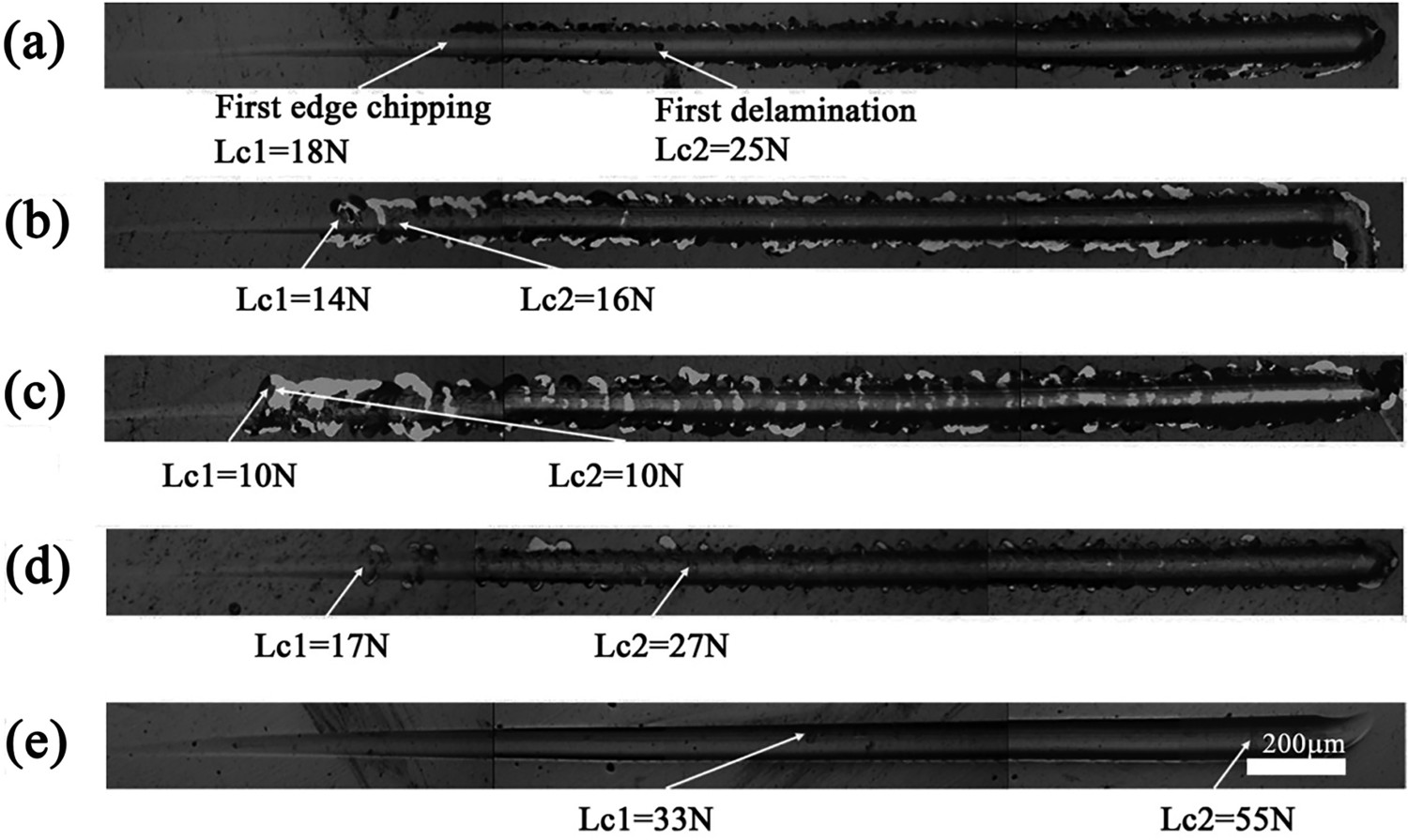
Figure 7 is the relationship between the hardness of TiN film and Ja. In order to ensure the accuracy, each sample was measured 5 times and averaged. As Ja increases from 0.14 to 0.24 A cm−2, a gradual increase in the hardness from 1006 HV to 1224 HV is observed. However, the hardness of TiN films increases rapidly to 1958 HV as Ja increases to 0.32 A cm−2. The rapid increase in the hardness can be mainly attributed to the formation of regular dense columnar grains in films as shown in Figure 4(d). TiN films prepared at 0.4 A cm−2 exhibit the maximum hardness of 2388 HV, which can be explained as follows. First, TiN films of 0.4 A cm−2 exhibit denser structures as compared to those of 0.32 A cm−2 (Figure 4(d,e)). Moreover, the decrease in the average grain size probably contributes to the increase in the films hardness, according to the Hall-Petch effect [18,19].
The relationship between the hardness of TiN films and Ja.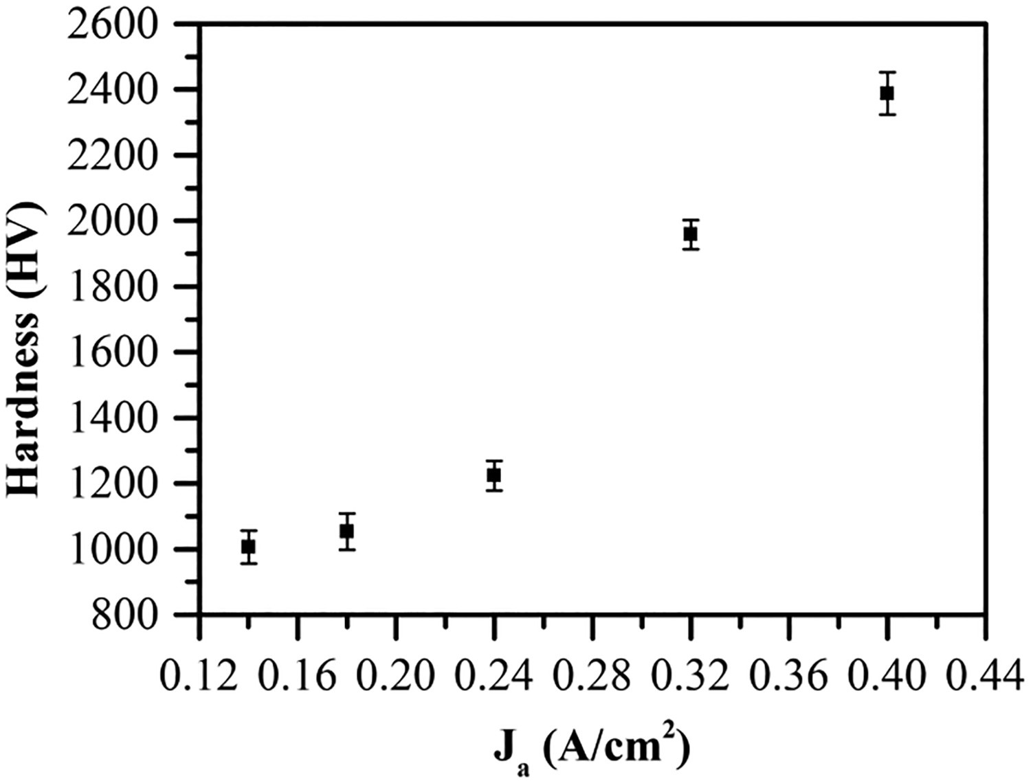
Conclusion
TiN films were deposited in the AGD and GATD region. The thickness increased with the increase in Ja, and the maximum average deposition rate was 110.4 nm min−1 at 0.4 A cm−2. Ji/Jfilm value varied from 0.23–0.28 in the AGD region, and increased rapidly from 0.37–0.48 as the Ja increased in the GATD region. It meant that the ionization rate of particles continued to increase as the increase in Ja, and the GATD particles had better ionization rates. The AGD TiN films exhibited pyramidal structures and many gaps between granules with low hardness and poor film-substrate adhesion. However, the GATD TiN films exhibited dense structures, good adhesion (up to 55 N) and high hardness (maximum of 2388 HV).
Footnotes
Acknowledgements
The authors gratefully acknowledge the financial support of the project from the National Natural Science Foundation of China (No. 51571114) and the Priority Academic Program Development of Jiangsu Higher Education Institutions (PAPD).
Disclosure statement
No potential conflict of interest was reported by the author(s).