
Abstract
The main scope of this work is the metallization of high density Acryonitrile Butadiene Styrene (ABS) surfaces for aerospace applications. Originality and main focused area of the study is to grasp the mechanism of physical properties of the surface and the effect of wet chemical processes on the surface of the ABS substrate. After surface sensitization and metallization with nano-sized ions, the polyurethane surface is metallized and nickel (Ni) coated with electroless and elecrolytic Ni plating processes. The ultimate goal of these advances is the production of composite lay-up tools for the production of primary and secondary composite aircraft parts from nanoscale to macro level. Composite lay-up tool requirements of the aerospace industry include a minimum thickness of 5 mm, acceptability of airtightness testing and reduced surface roughness. Results show that increasing current density adversely affects the surface morphology and metallization processes enhance the surface conductivity of the foam.
Keywords
Introduction
Composite manufacturing is significant for the aerospace industry because of preferred characteristics like enhanced strength/weight ratio, high durability limit under cyclic stresses and minimized corrosion issues of composites [1–10]. Composite parts are manufactured by several methods while the hand lay-up process is still used commonly. Thermoset resin impregnated carbon fibres (prepregs) are layed on each other by concerning symmetry and balance rules of composite manufacturing. Afterwards, the thermoset matrix is cured under high temperature and pressures in autoclaves. The aerospace industry uses low tolerances for composite part dimensions. Therefore, several composite lay-up tool materials exist related with the complexity of the parts. Thus, manufactured structures can follow limits of design tolerances. However, the most important problem for composite manufacturing is the thermal expansion coefficient difference between manufactured part and composite lay-up tool material [11]. This problem may result in delamination, spring-backs and distortion problems after the curing process. Related with these concerns, carbon-fibre reinforced composite, aluminium and invar (FeNi36/64FeNi) are recently used lay-up tool materials for composites in aeronautics [12]. Major drawbacks of these composites are low life-cycles, high coefficients of thermal expansion (CTE), high costs and waste occurence [13]. Thus, researchers are focused on the development of Ni lay-up tools via electrochemical methods since Ni has a rather mediocre CTE and is reliable under harsh environmental conditions [14]. Additionally, other important concerns about the tooling material are the thermal cycle durability and wear resistance [15]. Several studies related with the experimental investigation of the tool/part interface were conducted to determine durability and perform life cycle assessment [15–18]. Corresponding studies showed that Ni electroplating with sulphamate solution reveals lower damage to human health than four well-known different thermal spraying processes (wire-arc, plasma, high velocity oxygen fuel (HVOF) and cold spray) which is of signifance for manufacturers of aerospace platforms. Additionally, part production with nickel sulphamate ions contributes to low internal stress characteristics [16]. In the light of these information, the major aim of this study is to set up the fabrication of Ni lay-up tools for composites by virtue of electroforming on ABS surfaces. To the best of our knowledge, almost the complete literature focuses on the metallic substrate for electroplating processes for all applications due to the conductivity requirement of the electroplating process. Since there is a conductivity barrier between anode and cathode surfaces as well as a double layer formation of nickel ions, the electric field is changed directly. Within this regard, Shourije et al. [19] investigated and analysed the distribution of the electric field in a nickel-induced electrolytic cell within different electroplating conditions via COMSOL Multiphysics [20]. Major drawbacks of metallic substrates for aerospace tooling are the cost-effectiveness and manufacturing limitations. Moreover, purchase and manufacturing dimension limits for complex shaped metallic substrates for the electroplating process exist. Thus, the most effective solution is surface metallization of easily machined, transported, and cost-effective polymeric substrates [21].
The originality of this study is that it is the first study for the application of surface sensitization, activation, and electrolytic Ni plating on the surface of ABS for the aerospace industry. The covering metallization was performed stepwise by degreasing, etching, sensitization, activation as well as electroless nickel plating. In the case of sensitization by tin (Sn), complex colloids of an Sn sensitization blend contain mainly
Another important property of surface metallization of ABS is that it is also applicable for additively manufactured parts to improve relevant surface properties and especially the surface roughness [34–36]. Butadienes of the ABS structure are removed by chromic acid. Change of the surface roughness of the as-build sample after electroless and electrolytic Ni plating.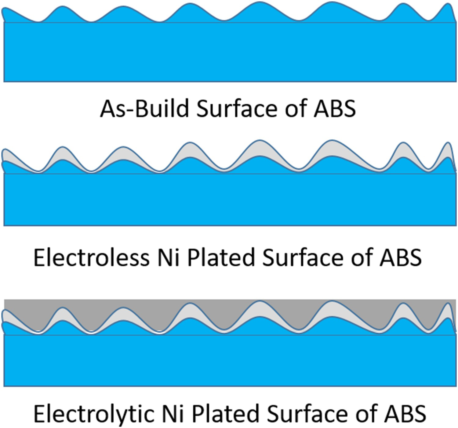
Within the concept of this study, the surface of the ABS substrate was metalized and plated with an electroless Ni electrolyte to bring the metallic layer on top of the surface of ABS for the preparation of the surface to electrolytic Ni plating. In addition, the final step is the electrolytic Ni plating. In this study, the effect of each metallization technique was examined before and after each metallization and plating procedure. By this route, the mechanism of metallization was examined with microstructural characterization such as; surface morphology, crystallography, elemental spectroscopy methods and electrical characterization via the Hall effect measurement method. Finally, the composite lay-up tool manufactured from the electrolytic Ni plating procedure was obtained. Additionally, this study broadens the horizon of improving surface properties of additively manufactured polymeric parts and manufacturing hollowed structures of metallic parts from polymer additive manufacturing approaches like Fused Deposition Modelling (FDM).
Material and methods
Materials
An ABS substrate manufactured by injection molding with a minced surface roughness of 0.9–1 μm was used. The surface of neat ABS was cleaned and degreased with alkaline (sodium hydroxide (NaOH)) and acidic (chromium(III) oxide (
Experimental procedure
Metallization of the ABS surface is a multistep process. Since the main purpose of the present manuscript is to grasp effects of acceleration and neutralization processes on the metallization mechanism, characterization was also applied on intermediate steps.
After the alkaline and acidic cleaning processes, the surface of ABS was available for neutralization and the subsequent acceleration process before sensitization and activation steps. The neutralization stage involved removal of residual chromium from the etching solution by sodium sulphite which is a reducing agent in the solution. Surface sensitization was conducted by submerging the foam into a blend consisting of 50
The effect of the activation approach was conducted in the mixture of both Pd and Sn solutions. The main reason for this process is the intentional constitution of butadiene removal of the acidic etching process with chromium and sulphuric acid solutions. Remarkably, there were microporous regions of removed butadiene positions [40]. The final step was acceleration. The mixture of sodium hydroxide, copper(I) sulphate and EDTA was used as dissolution of 


Characterizations
Surface microviews of the substrate at each step were observed by a Scanning Electron Microscope (SEM) with the brand FEI 430 Nova NanoSEM. Electrical surface conductivity analyses were performed by a Hall Effect Measurement System NanoMagnetics Instruments ezHEMs. Elemental spectroscopy on the top of the surface (approximately 10 nm) was done by a PHI 5000 X-ray photoelectron spectroscope (XPS). Crystallography analyses were performed by the PANanalytical X'Pert Pro X-ray Diffractometer (XRD). Surface tribology analyses and wear rate measurements of electroless Ni plated, non-activated and activated samples were determined with the Tribotechnic Pin-on-Disc & Oscillating Tribometer device. Samples were prepared and analysed according to ASTM C1624 and G171 standards. The effect of the acceleration process on the surface metallization process was examined. After subsequent metallization procedures, electroless and electrolytic Ni-plated samples were analysed with the pin-on-disc method, and surface hardness measurements were conducted with the Zwick Micro Vickers tester under 0.3 N load. Nickel-plated samples mounted on a rotating disc and an aluminium oxide (
Results and discussion
Microviews, grain sizes, elemental spectroscopy analysis and morphologies of the coatings were analysed by SEM. 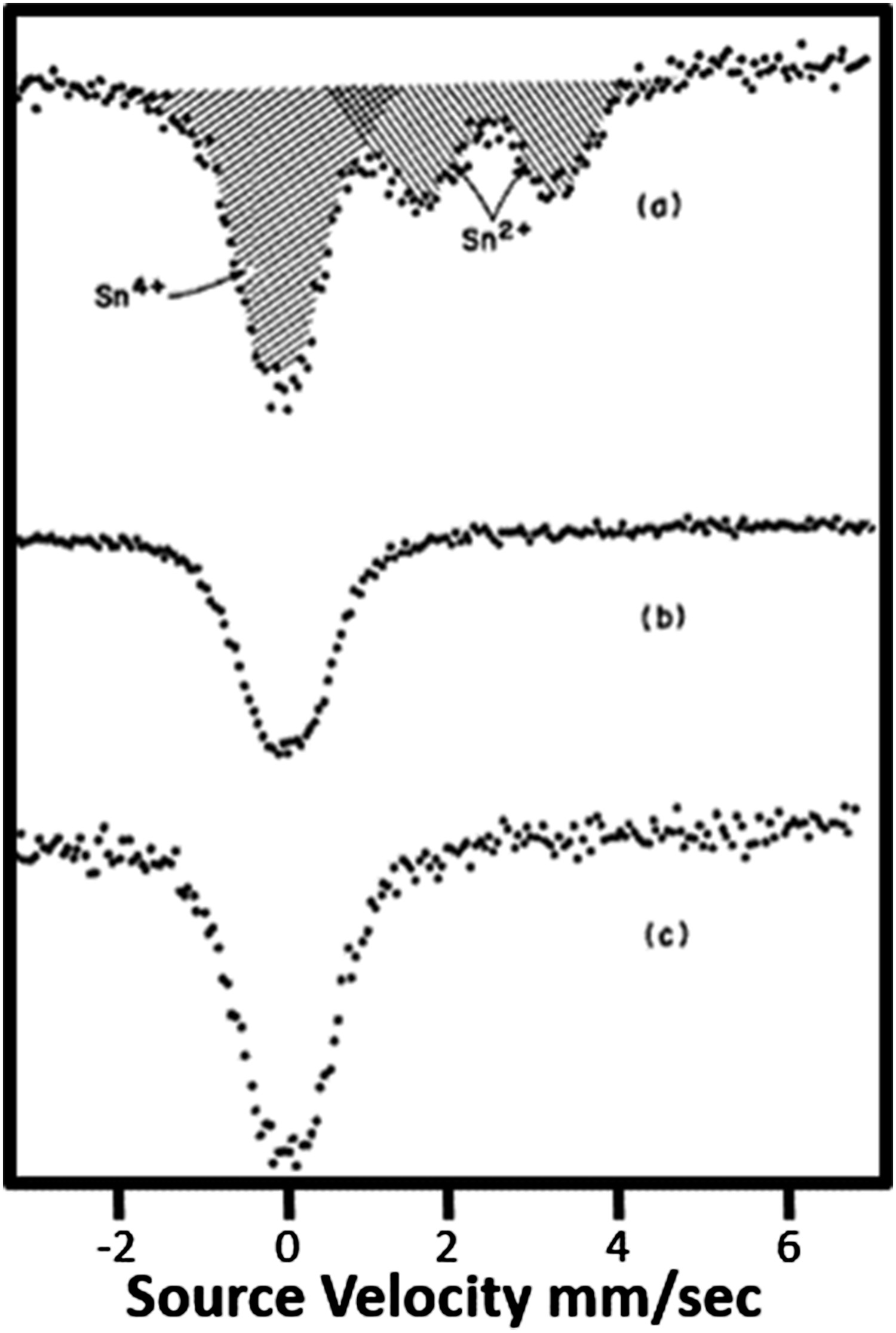
The surface of ABS was metallized after electroless Ni plating. Thus, the subsequent plating process was applied on the Ni surface. Current efficiency values after each metallization process were calculated from Faraday's law for electrochemistry [31].
The pH of the commercial alkaline electroless plating electrolytes decreases during the plating procedure. Therefore, alkaline electrolytes loose their stability in time [43]. This unstable condition results in suppression of the stability of the approach and all Ni ions inside the electrolyte are reduced suddenly [43, 44]. However, in the chosen acidic electrolyte, the reduction of Ni ions is continuous and homogeneous in comparison to commercial alkaline electrolytes.
After each surface metallization process SEM analysis was performed. Surface quality and grain size of Ni atoms after the electroless Ni plating process are given as Figure 3. The uttermost adequate surface was measured for the electroless Ni plated surface after neutralization and activation. Grain size and surface morphologies of the surface of ABS is decreased. NAA (Nucleated Activated and Accelerated samples) in Figure 3(e–g) show finer grain sizes in comparison to NA samples. However, the corresponding current efficiency is lower. Thus, usage in industrial applications is not preferable in this case.
SEM images of electrolytic Ni plated surfaces of ABS substrates. ABS substrates were subjected to neutralization and activation with current density values at (a) 2, (b) 3, (c) 4, (d) 5 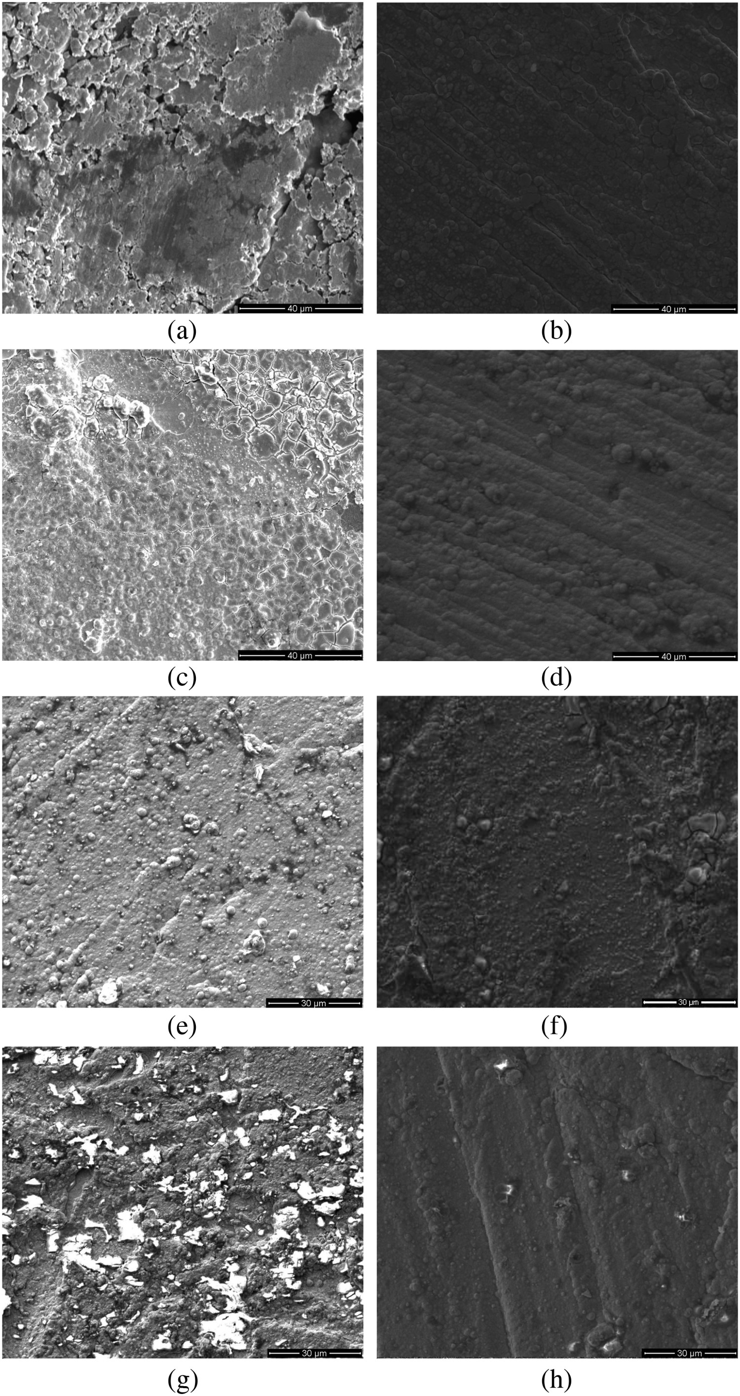
Furthermore, this study investigates the outcome of the acceleration process on surface metallization and coating efficiency performance of the coatings. Surface finish and current density related efficiency calculations determined by thickness measurements from cross-sectional SEM images can be seen as Figure 4. The theoretical thickness of the sample is 250 μm. The theoretical value and average data of the experimental results are being compared while current efficiencies were calculated in detail. Results indicate that neutralization and activation processes are fairly enough and can be easily seen in Figure 5. Additionally, the acceleration process does not affect current efficiency as expected due to the expectation of improvement in the electrical conductivity values which is explained below in detail. As a result, the optimum processing parameters are 3 Cross sectional SEM analysis of the neutralized, activated and accelerated sample with a current density of 3 Effect of current density with/without acceleration process after neutralization and activation.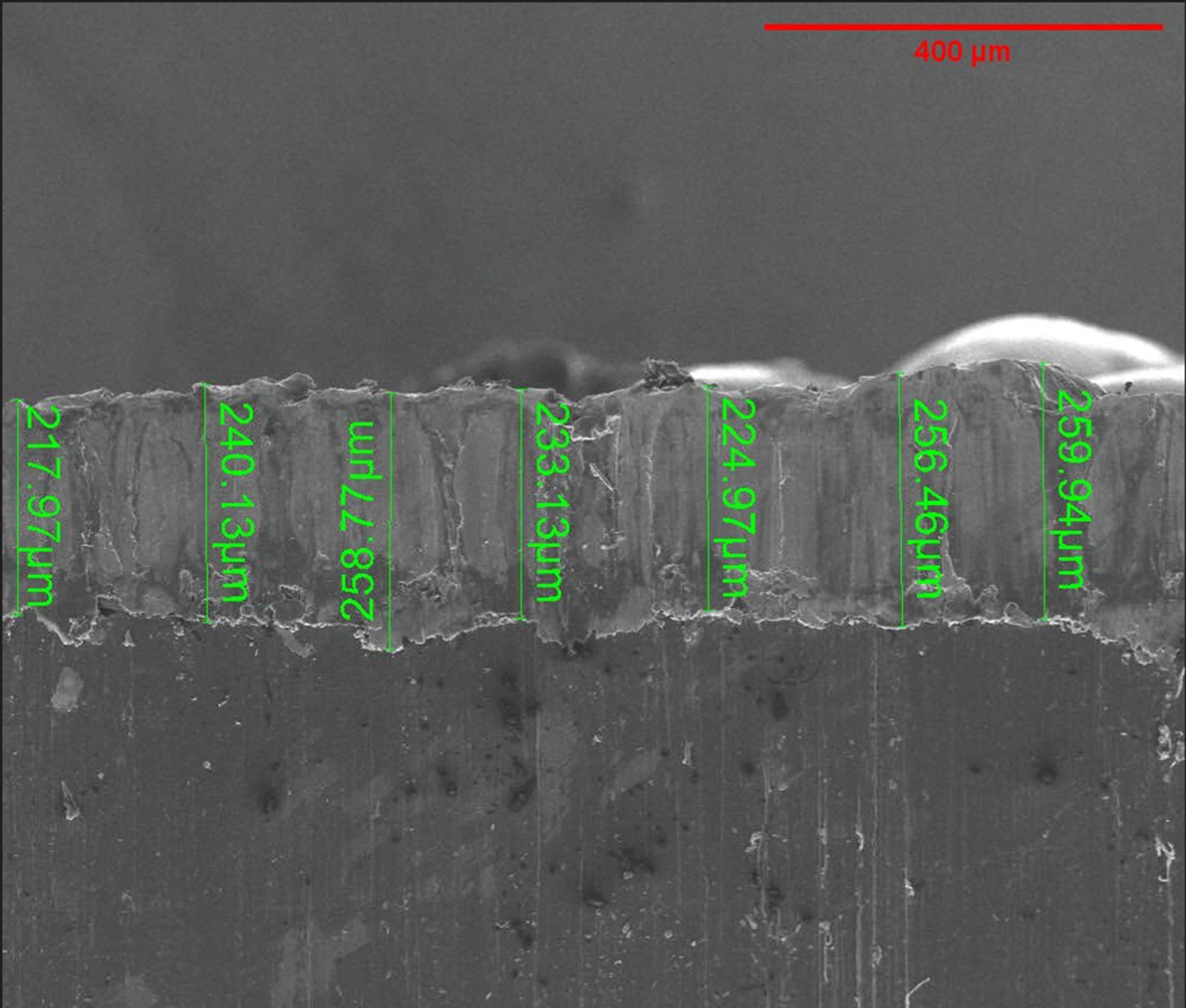
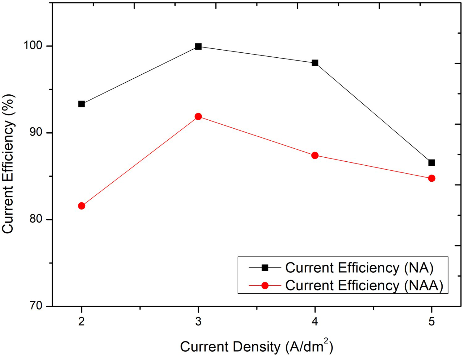
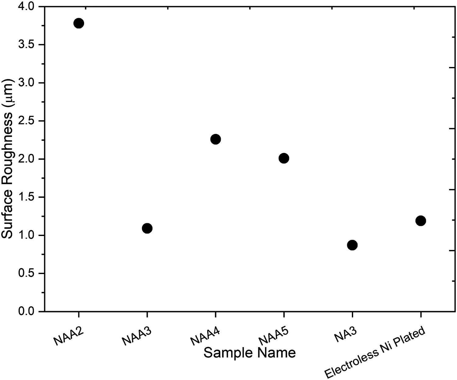
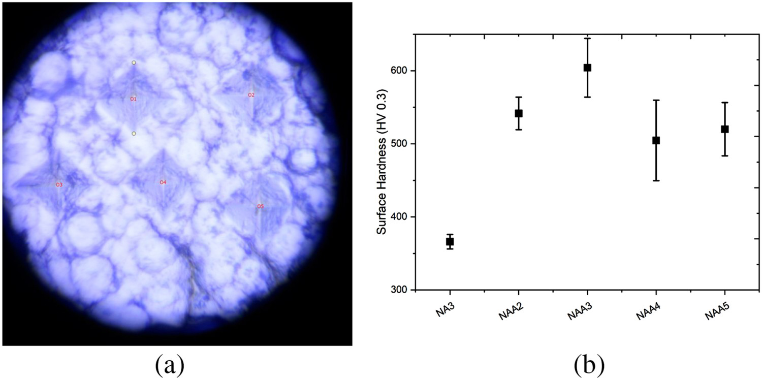
The tribological behaviour of electroless and electrolytic Ni plated samples was determined by wear analyses, surface hardness measurements and surface roughness analyses. Adhesion behaviour and surface integrity of Ni on the surface of ABS were measured to analyse the performance of the Ni lay-up tool under variable environmental conditions depending on the reutilization of the tool after each curing procedure. Pin-on-disc measurements were conducted on neutralized, activated, accelerated, electroless and electrolytic Ni plated samples coated with 2, 3, 4 and 5 Effect of acceleration process on electrolytic Ni plating with 2, 3, 4, 5 Surface roughness analysis for the activated and Ni plated specimen; activated, accelerated and Ni plated samples with 2, 3, 4, 5 (a) Optical image of the surface hardness measurement with a standard deviation obtained for 5 different hardness values and (b) results of activated, accelerated and electrolytic Ni plated samples with current densities of 2, 3, 4 and 5 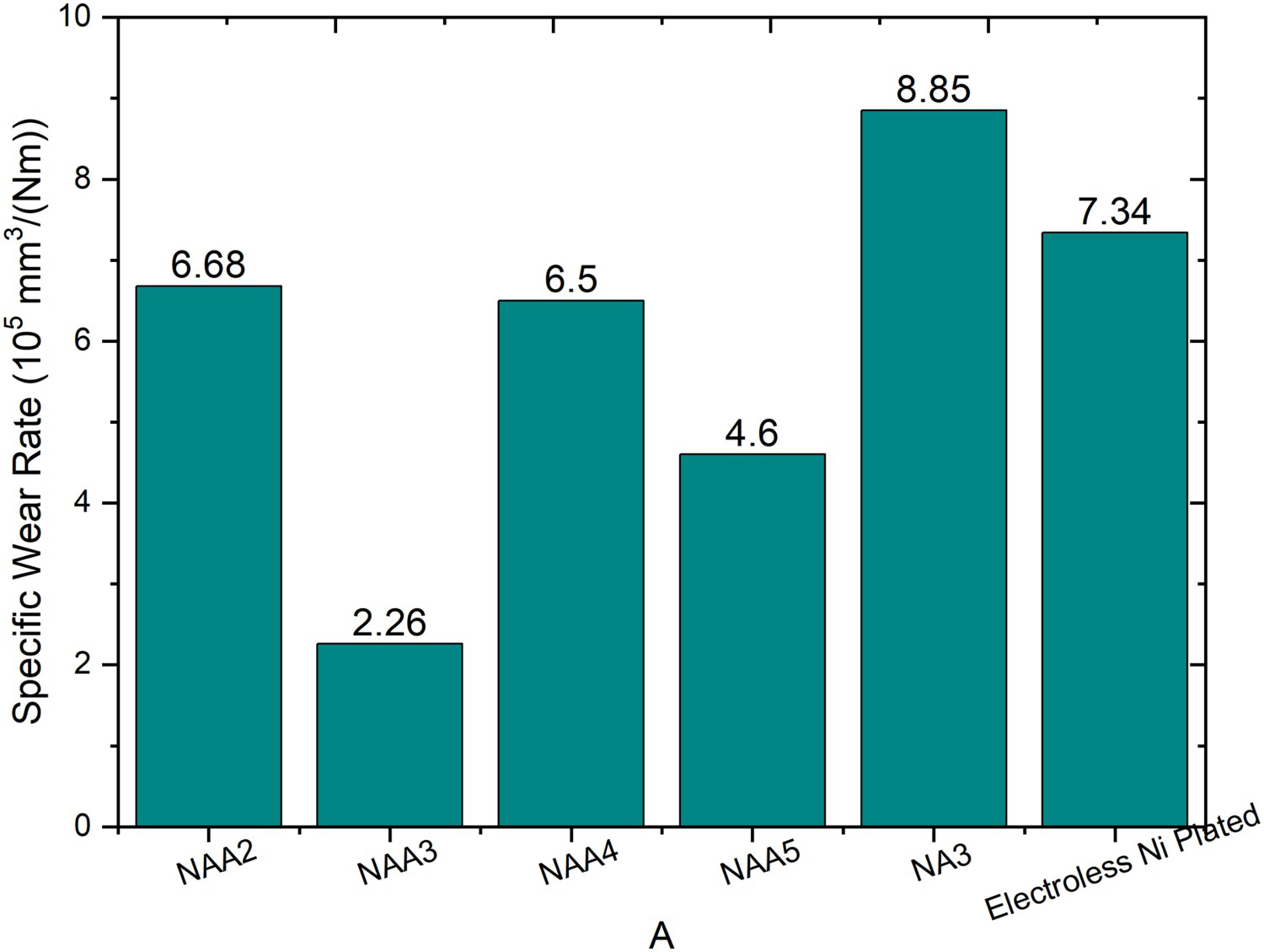
Additionally, XRD was conducted for electrolytic Ni plated specimens at 2, 3, 4, 5 Effect of current density on crystallographic orientation with/without an acceleration process after neutralization and activation.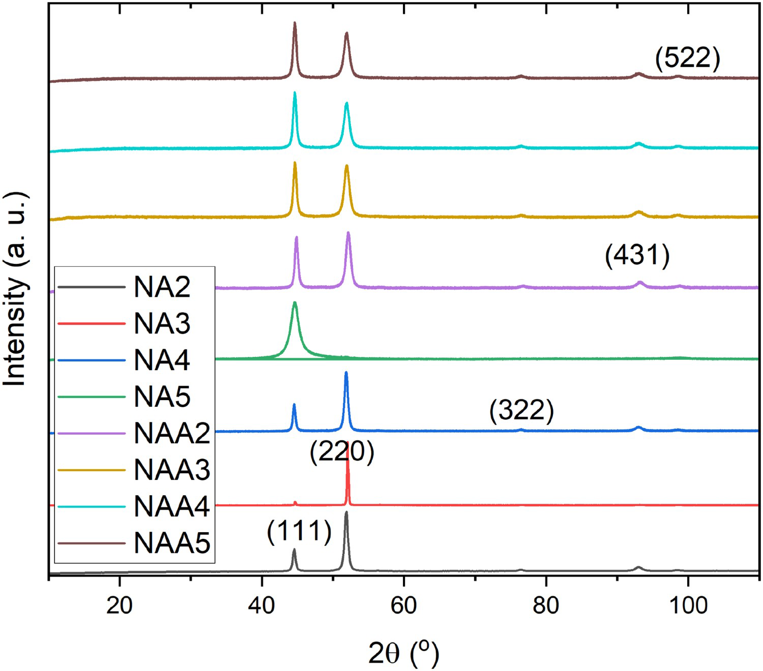
Results subsequent to the electrolytic Ni plating after each metallization step can be seen in Figure 9. Examination and optimization of process parameters reveal the influence of acceleration on crystallographic arrangements. The strongest reason for the acceleration process is to dissolve excess Sn from the surface to remove adsorbed Pd. Yet this problem is overcome by dissociating Pd and Sn into the activation bath and firstly sensitizing with Sn ions and activating only with Pd. With the help of this procedure almost all of the
XPS analyses were conducted for each sample after the electroless Ni plating procedure. Results can be seen in Figure 10. P2p and Ni2p peaks occur due to the use of hypophosphate as reducing agent and electroless Ni plating, respectively. Sn and Pd are not observed since the surface was fully dense in contrast to the literature [14], where foam substrates were examined after the final plating step. However, XPS measurements of this study where performed after acceleration and electroless Ni plating. Thus, presented graphs in Figure 10 display intermediate process results which explains the absence of any Cu peaks while the literature contains results after the final step for foam substrates [14].
Examination of the effect of acceleration process on the electroless Ni coating by XPS.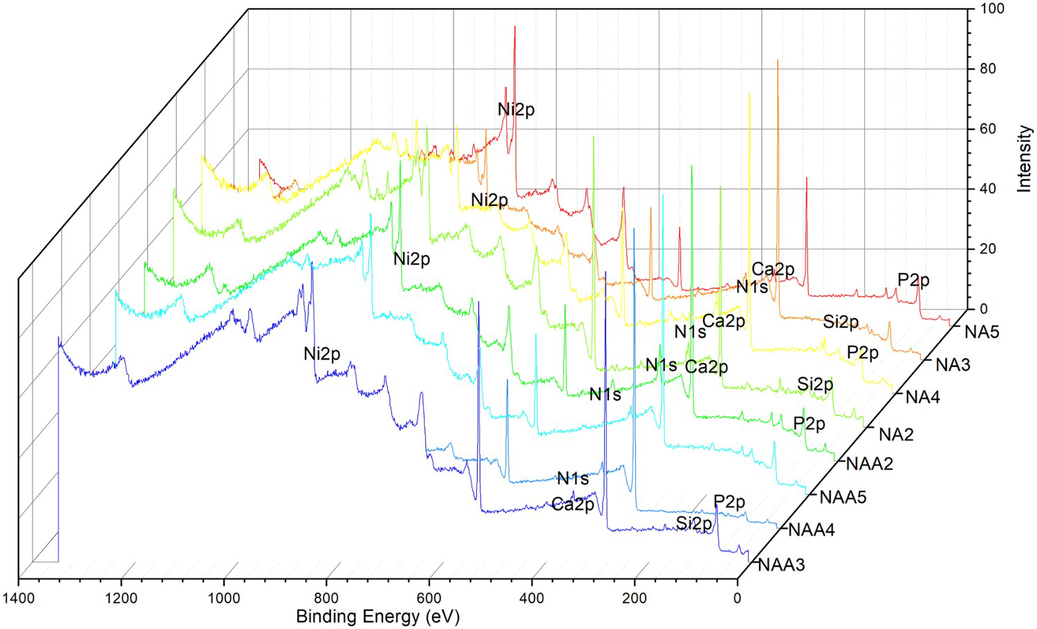
BET analyses were conducted for electroless as well as electrolytic Ni plated samples and as received ABS as can be seen in Figure 11. The specific surface area was measured by analysing the cross section area of nitrogen molecule. Nitrogen adsorption is the key parameter for the measurement of specific surface area. Results show that application of electroless Ni plating increases the specific surface area of the sample. This result can be explained by the butadiene removal process after the etching while the corresponding space was not filled by Pd ions and thus Ni atoms after electroless Ni plating. In addition, the specific surface area of electrolytic Ni plated surface is decreased as expected since the corresponding pore density is reduced.
Specific surface area of bare ABS, electroless and electrolytic Ni plated surfaces.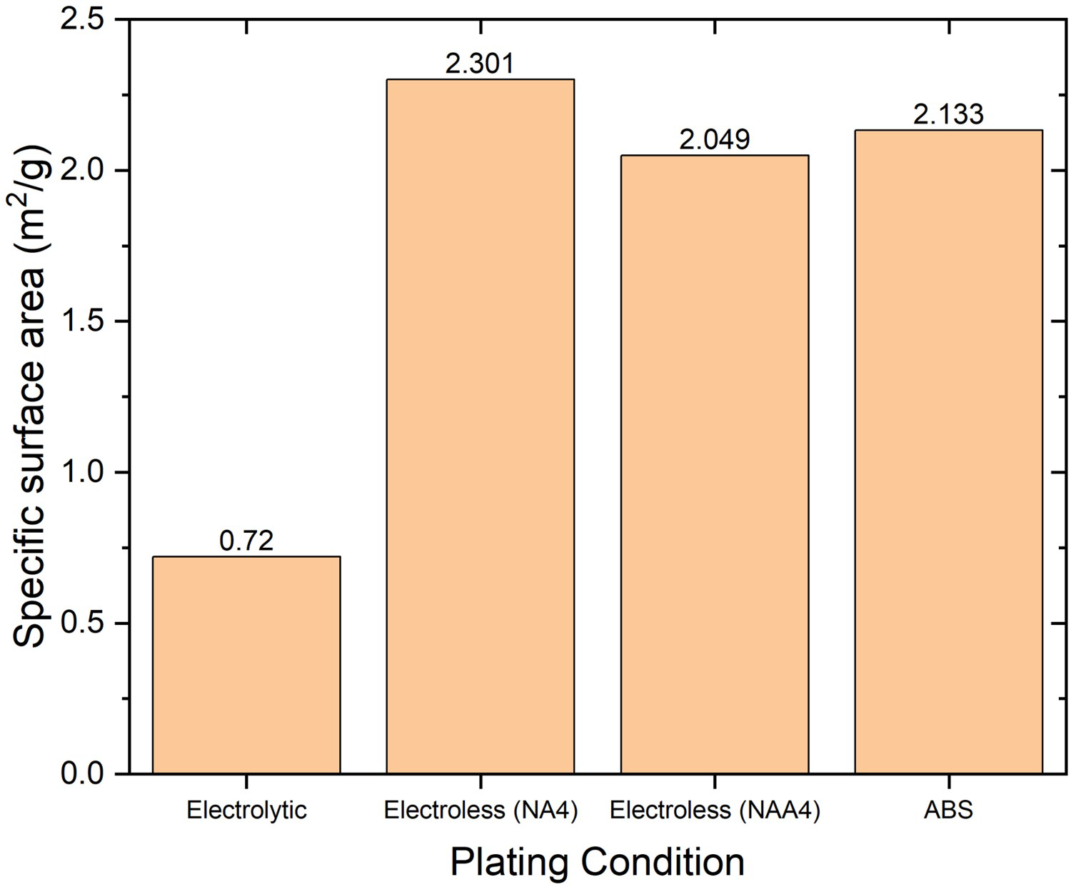
Effect of electrical characterization of Ni plating after each electroless plating process.
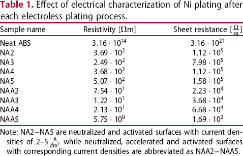
Note: NA2−NA5 are neutralized and activated surfaces with current densities of 2–5
Conclusion
The major objective of this presented manuscript was to define the metallization mechanism of ABS and grasp the behaviour of the coating parameters at each step. Several characterization techniques were applied for the analysis of surface metallization. The effect of activation after sensitization process, pH on the electroless Ni plating behaviour and also affects of current density values on the electroless Ni plated samples were analysed. An efficient surface quality was obtained by the neutralized surface without acceleration process. The highest electrical conductivity was obtained with the electroless Ni plated specimen in the acidic electrolyte with higher Pd amount. Moreover, Sn sensitization, Pd activation as well as electroless Ni plating in the acidic electrolyte are necessary steps before the electrolytic Ni plating for lay-up tool manufacturing.
Footnotes
Disclosure statement
No potential conflict of interest was reported by the author(s).