






Abstract
In the era of proliferated distributed renewable energy sources, high-gain DC–DC converters dragged much attention among the researchers. But there is a concern that high-gain converters have less efficiency and high switching stresses. The converter topology has two quasi-impedance source network and a voltage multiplier cell unit to facilitate very high-gain output voltage. This work also suggests using a non-linear carrier controller which embodies two loops within it: one facilitates the input variations and the other loop assists load regulations. The input variations due to varying irradiation of photovoltaic are alleviated by employing the perturb and observe maximum power point tracking mechanism. The simulation of the work is realized in MATLAB/Simulink arena, and hardware circuits are validated using the dsPIC30F4011 controller. This paper proposes a new two-loop control embedded high-gain DC–DC converter fed by photovoltaic source which aims at encouraging the project-driven engineering education teaching and thereby inherently complying to the standards set for academic excellence through Bloom’s taxonomy.
Keywords
Introduction
Engineering education should hone the skills of budding engineers and technocrats to design, develop, innovate, and invent new engineering appliances. The pedagogical style has been changing over the years though the rudimentary way of teaching still persist. But core engineering subjects like electrical, mechanical, and civil need to be taught to the undergraduate level students in such a way that the concepts are realized and understood practically. The conventional way of theoretical teaching alone may not go well with core concepts of engineering, as the students find it hard to remember the theoretical nuances. In electrical engineering, especially there is a huge scope for the students to understand the concepts of power engineering by realizing a prototype, animated simulation, or through a demonstration of working model. The cognitive levels such as knowledge, understand, apply, analyze, synthesis, and evaluate are really tested in realizing a concepts by simulation model or hardware prototype. This way of making the undergraduate students to understand electrical engineering concepts facilitates a well-groomed company-ready engineering graduate, a student with more industrial relevance. In all, the project-based learning makes the student confidence to face the real-time problems. Also, it complies with the Bloom’s taxonomy which emphasis on academic excellence. This project-based learning can be made pragmatic when the students do their laboratory experiments with full understanding. Also, when budding engineers get involved in experiment/project-based learning, they not only evolve as good engineers but also good managers. Engineers become very good managers when they get involved in team work, tasks being delegated, and handling the finance of the project. In recent past, there prevails a lot of encouragement to the students to get involved themselves in minor project when they read subjects like power electronics, micro-controller, and electronics devices. Power electronics and micro-controller are the two indispensable subjects that an undergraduate student should be strong with, to aspire a job in power industries. The study associated with this article relates to the teaching concept of high-gain DC–DC converter which is a contemporary topic in power electronics. The whole world is shifting its attention towards distributed energy resources as the conventional way of interconnected system finds difficult to accommodate the power interaction through renewable power sources. This paper suggests using photovoltaic (PV) power as the source for the proposed power electronic circuitry. PV sources are made compatible to the load only through power electronic interfaces. The high-gain power electronic interface is a novel one in this work. The undergraduate students are initially taught with the basic DC–DC converters like buck and boost converters and an innovative topology is then developed. The real-time work of the students in bringing out a PV fed high-gain DC–DC converter is presented in this paper and the students responded well in bringing the paper into a research paper. This real-time work can be related with the work done as major project in final (eighth) semester or as a minor project in lower semesters. The most reliable style of engineering pedagogy of prototype realization is done in this work. The following paragraphs give a literature note on the presented work.
It is evident that there prevails a glooming power crisis around the globe 1 and in recent past much emphasize has been given on utilizing sustainable sources to alleviate the power deficit problem. Among the sustainable sources the most coveted is the PV resource which has peculiar advantages like portable, scalability, etc. compared to its other equivalents. PV as such, being intermittent in nature, demands the role of power electronic interfaces mandatorily.2–5 Also to make most out of the existing power in PV in a given point of time, along with the power electronic converters intelligent control schemes called maximum power point tracking (MPPT) are required.6–9 These MPPT controllers work effectively to deliver the maximum power available in the PV to the load for varying environmental (irradiation and temperature) changes. 10 In the research forum, numerous research articles on MPPT algorithms have been documented already.11,12 The category of MPPT scheme can be classified predominantly according to the complexity of the algorithm, control parameters involved, interfacing power electronic topologies, etc.13–16 Amid the well-known MPPT control techniques, the most coveted ones are perturb and observe (P&O), and incremental conductance (INC), as these two algorithms are complementary in nature and cater the need of application in which it is employed. P&O algorithm which works on iterating the power and voltage values in power–voltage (P–V) curve to find the exact operating point (Vmpp, Impp) at which the PV delivers maximum power. This algorithm is a simple cost effective one compared to its INC counterpart. On the other hand, INC needs comparatively an extended competency in executing the algorithm and in this way P&O is preferred over INC in most of the PV applications. 17 In this work, the simple P&O MPPT is adopted to regulate the PV power for its respective change in irradiation and temperature.
The major bottleneck that PV systems have in interacting with the grid/load is the voltage matching issue. 18 PV panels, though available in different power ratings, have voltage levels confined in the 17–40 V range. A typical 250 W panel may have a maximum voltage of 36 V, and therefore the DC–DC converter which interfaces PV panel and inverter loads (AC loads) drags utmost importance. The various traits of DC–DC converters like gain, efficiency, topologies (isolated and non-isolated) have to be chosen vigilantly in PV power system. 19 ,- 20 The step up DC–DC converter say, boost converter is the rational choice in many applications where the load voltage will be several times the source voltage. The idea of configuring the panels in series to make up the voltage to an extent may also go as a futile idea if there is a mismatch between panels due to inhomogeneous exposure of sunlight on the PV panels in an array. Therefore, the choice of high-gain DC–DC converters is apt for PV applications and this high-gain converter can be isolated or non-isolated one. Non-isolated converters are much more preferred over its isolated equivalent due to the disadvantages like increase in size, losses and less efficient, voltage spike issues, etc. 21 To put in nutshell, the total efficiency of a typical PV –DC–DC converter- Inverter- /Grid/ Load system is primarily decided at the DC–DC conversion stage. In this context, exploring the research aspects in high-gain DC–DC converter with new topologies is highly prudent. The contemporary DC–DC converters quite often prevail when there is variation either in load or source; performs load or line regulation by a single voltage control loop. But the competency of the converter regulation faces a litmus test when there is a simultaneous variation in source and load. 22 In this research work, an innovative DC–DC circuit with effective two-loop voltage controlling mechanism has been developed. The DC–DC converter is fed by a PV system which has inherent variations in the source side due to its intermittent nature. The two-loop control system aided controller is capable of regulating the load voltage when there is a variation in load side.
Hence, by suitable preparation during the course, the students/researchers can carry out the design and develop stages in a teamwork project. The paper is so arranged that the next section presents the working and topology description of the proposed converter which is followed by a section that explains the control strategies elaborately. Then, the results are presented in the Results and discussion section. Finally, concluding remarks are given in the Conclusion section.
Proposed single switch hybrid DC/DC converter and analysis
The proposed DC/DC converter integrates two quasi-networks (continuous conduction quasi-impedance source (qZS) and discontinuous conduction qZS) and a single stage voltage multiplier for PV power generation system as shown in Figure 1. Three inductors (L1, L2, and L3); four capacitors (C1, C2, C3, and C4); two diodes (D1, D2) form the Z source converter, and inductor (L4); capacitors (C5 and C6); diodes (D3, D4, and D5) form the voltage multiplier circuit. Moreover, it inherits the additional merits such as common input and output ground, continuous input current, buck or boost of the input voltage by varying the duty cycle D.

Proposed DC/DC converter for PV power generation system.
Analysis of the proposed converter
The proposed converter is analyzed by assuming that the components employed are ideal, the capacitors are sufficiently large enough to provide constant voltage and the converter operates in continuous conduction mode (CCM). The operating modes of the converter with current flow path are shown in Figure 2.

Equivalent circuit of the proposed converter with various current flow paths: (a) Mode I and (b) Mode II.
Mode I (DTs)
Figure 2(a) demonstrates the equivalent circuit of the proposed converter in first operating mode. During this mode, the boost switch S is ON, whereas the diodes D1–D3 and D5 are in OFF state. The time interval of this mode is assumed as DTs. The panel output voltage VPV and the capacitor C1 discharges the energy to the inductor L1. On the other hand, the capacitors C2– C6 charge the inductors L2, L3, and L4. Voltage drop across of the C7 appears across the load. By applying Kirchhoff’s Voltage Law (KVL), the potential drop across inductors L1–L3 can be stated as

On account of the symmetric nature of L2 and L3, C3 and C4, voltage across these components are given by

Mode II ((1–D)Ts)
Figure 2(b) demonstrates the equivalent circuit of the proposed converter in second operating mode. During this mode, the boost switch S is OFF, whereas the diodes D1–D3 and D5 are in ON state. The time interval of this mode is assumed as (1–D)Ts. The panel output voltage VPV charges the inductor L1 and the energy stored in the inductors L2, L3, and L4 discharges via the capacitors C1–C6 to the load R. By applying the circuit, the potential drop across various components can be stated as

The output voltage gain is acquired by applying the voltage-second balance principle on the inductors L1, L2 (or L3), and L4, and we have



Solving equations (4) to (6) by substituting equations (1) to (3), the potential drop across the capacitor is given as




Voltage multiplier is used to boost the static gain of the converter by (X + 1), where X is the number of multiplier cells connected.
23
Here, a single cell voltage multiplier (C = 1) is connected in series with the DC/DC converter to boost the output voltage. Thus, the output voltage is given by

The gain of the converter is

Inductor design
The expression for the inductor can be derived by assuming the current ripple (ΔI) to an allowable limit. During CCM operation, the following expressions can be deduced


Substituting equation (14) in equation (13), the expression for the inductors L1–L3 are given by


Capacitor design
The expression for the capacitor can be derived by assuming the voltage ripple (ΔVc) to an allowable limit. During CCM operation, the following expressions can be derived

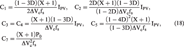
Substituting the values of ic and ΔVc in equation (17), the expression for the capacitors C1–C5 and C7 are given by
Comparison of gain and voltage stress
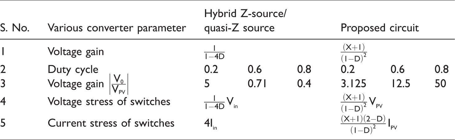
The boost ability of the converter can be testified by comparing the performance of it with the well-entrenched topologies. Thus, the variations of the voltage gain with respect to D have been studied for various converter topology in the literature24–28 and also been compared with the proposed. Various performance parameter comparisons with the existing hybrid qZS topology 28 are tabulated in Table 1.
Comparison of various parameters with the existing high-gain converter, as listed in HanyunShen. 28
Control strategy
The control technique of embedded proposed high-gain converter is schematically presented in Figure 3. It consists of essentially two control loops, one at the source side and other one at load side. P&O algorithm known for its simple execution and reliable operation is employed in this work to enhance the power delivery capability of the PV structure when it is exposed to varying environmental conditions. The load side regulation is achieved through a dynamic carrier voltage regulation which alleviates the load intermittencies.

Control techniques of proposed converter.
P&O algorithm
Since its inception, P&O algorithm remains to be very compatible for many applications. In this algorithm, small change in the control signal of the power converter is occasionally introduced in the array voltage or current with respect to the output power of the previous cycle. If the rate of change of output power with respect to panel voltage increases positively (dPPV/dVPV> 0), then the path for attaining the operating point moves in one direction and vice versa. If the perturbation rate is selected vigilantly, the oscillations in the power output are so meek.
Non-linear carrier controller
Non-linear carrier controller (NLCC) known for its application in rectifiers to improve power factor is used in this work. It has some remarkable advantages like meek stability issues and very high dynamic response. 29 The following section explains how the switching pulses are generated. The switching pulses are developed by comparing the reference current from MPPT controller and current flowing through the switch. Two integrators facilitate the generation of parabolic carrier wave. It is then compared with the integrated error in voltage which is of ramp shape. The peak value of the ramp is proportional to control signal for regulating the load voltage. The time duration of parabolic waveform decides the duty cycle of the MOSFET.
Results and discussion
The performance of the proposed high-gain DC/DC converter with P&O MPPT algorithm and NLCC technique is simulated using the Matlab/Simulink and experimentally realized with the dsPIC30F4011 controller with the parameters listed in Table 2. The values for inductance and capacitance are determined by having the criteria of 5% output ripple as per the IEEE standards. The converter is tested with the various uncertain conditions like varying irradiation and varying load scenario. The following subsection gives the detail about it.
Parameters.

Proposed converter with P&O MPPT algorithm
When solar panel feeds the proposed converter, the high-gain converter amplifies the output voltage waveform corresponds to the irradiations. Typically for 0.95 SUNS irradiations, 17.8 V is amplified to 210 V which is shown in Figure 4(a). Figure 4(b) and (c) demonstrates the corresponding current and power waveforms, respectively.

Proposed converter output: (a) voltage waveform, (b) current waveform, and (c) power waveform.
Simulation voltage and current waveforms of the each element in the circuit for a duty cycle D = 0.45 is shown in Figure 5. Figure 5(b) demostrates that the inductor currents iL1, iL2, iL3, iL4 are in continous conduction mode. Also, it can be inferred from the figure that ripple in the inductors are very low as it is connected between the capacitors. The voltage across the diode D4 is shown in Figure 5(c). Similarly, the voltage across the diodes D1, D2, D3 are shown in Figure 5(d) to (f), respectively. From the figures, it can be concluded that diodes D1, D2, D3 are in complement state of operation with D4. The current flowing through the capacitor C7 is shown in Figure 5(d). Hardware results of the simulated waveform is shown in Figure 6. The extracted hardware results are in line with the simulated one.

Simulation waveform of (a) switching pulse; (b) L1, L2, L3, L4 inductor current; voltage across the diode (c) D4, (d) D1, (e) D2, (f) D3, and (g) C7 capacitor current.

Hardware waveform of (a) voltage across the diodes D1, D2, switching pulse, (b) C7, L2, L3, L4 inductor current, and (c) voltage across the diodes D3, D4.
Proposed converter with P&O MPPT algorithm and NLCC
NLCC-based contol results are discussed in this section. The controller has been designed to maintain the constant voltage of 200 V, irrespective of line and load pertubations. The initial load is considered as 500 Ω for 1 SUNS irradiations. Whenever the change in the irradiations occurs say 1.02 SUNS, the V0 of the converter will increase. Thus, V0 is measured and it compared with the Vset, thereby the error in voltage Ve(t) is calculated. Then, the error in current through the switch is converted to its equivalent voltage Vc(t) with the capacitor C. It serves as the reference signal for this operation. The test setup of the proposed converter is shown in Figure 7.

Test setup of the proposed converter.
The versatility of the controller is tested for varying loads. The load resistance decreases from 500 Ω to 490 Ω, the load current increases from 0.35 A to 0.3675 A, and as a result, a dip in the voltage occurs. The controller tries to regulate the voltage to the set value by adjusting the duty cycle of the switch “S”. Its corresponding voltage and current waveforms are shown in Figure 8. To check the versatality of the controller, the load resistance is decreased from 500 Ω to 430 Ω, and from Figure 9 it is explicit that the voltage is regulated to the desired level.

Output waveforms for change in load from 500 Ω to 490 Ω: (a) voltage and (b) current.

Output waveforms for change in load from 500 Ω to 430 Ω: (a) voltage and (b) current.
Figure 10(a) and (b) shows the simulation and hardware output voltage waveform of proposed converter with line-load regulation, respectively. The change in solar irradiation is introduced at 0.3 s. As irradiations vary, the output voltage of the converter increases from 200 V to 215 V, and in simulation it settles in 0.06 s, whereas in hardware it increases from 200 V to 214.5 V and settles in 0.078 s.

Output voltage waveform of proposed converter with line-load regulation: (a) simulated and (b) hardware.
Figure 11 represents the output current waveforms with line-load regulation. In simulation, because of the raise in solar radiations, the output current increases from 0.35 A to 0.38 A at 0.3 s and settles at the normal value in 0.06 s, whereas in hardware current it increases from 0.345 A to 0.386 A and settles at 0.078 s. The load resistance decreases from 500 Ω to 450 Ω, the load current increases from 0.35 A to 0.39 A and due to this the dip in voltage occurs. In simulation, the step change in load is introduced at 0.6 s thereby the voltage decreases from 200 V to 190 V and settles in 0.1 s to its set value. It is noteworthy that in hardware setup within 0.15 s, the load regulation is achieved for a dip from 200 V to 188 V.

Output current waveform of proposed converter with line-load regulation: (a) simulated (b) hardware.
Compared to the simulation, the settling time is higher in hardware because of self-parasitic nature of the components. From Figures 10 and 11, it can be concluded that the simulation and hardware results were in line with each other. Also, the comparison of efficiency with various converter topology listed in the literature30–35 is shown in Figure 12. It is inferred that the proposed system has higher efficiency than the topologies presented in the literature.

Conclusion
Therefore, in this work, a new high-gain converter topology aided with effective NLCC-based two-loop control mechanism is proposed. The non-linear carrier control algorithm employed here regulates the load voltage with source intermittent P&O algorithm with closed-loop control. The whole system is realized in simulation and extended to hardware. The results reveal that suggested high-gain topology cuddled NLCC is very reliable for renewable applications. The same can be extended for multi-input fed topologies.
The conclusive remark is that students understand electrical engineering concepts when they are exposed to project-based learning. In this work, the described simulation and hardware realization schemes can be easily understood by undergraduate students.
Footnotes
Declaration of conflicting interests
The author(s) declared no potential conflicts of interest with respect to the research, authorship, and/or publication of this article.
Funding
The author(s) received no financial support for the research, authorship, and/or publication of this article.