






Abstract
This paper reports development and thermal characterization of tin-capped vertically aligned multiwalled carbon nanotube array composites for thermal energy management in load-bearing structural applications. Three-omega voltage measurements are used to characterize thermal conductivity in the vertically aligned multiwalled carbon nanotube-epoxy composites as well as in its individual constituents, i.e. bulk epon-862 (matrix) and tin thin film in the temperature range 240 K–300 K, and in individual multiwalled carbon nanotubes at room temperature taken from the same vertically aligned multiwalled carbon nanotube batch as the one used to fabricate the carbon nanotube-epoxy composites. A 1-D multilayer thermal model that includes effects of thermal interface resistance is developed to interpret the experimental results. The thermal conductivity of the carbon nanotube-epoxy composite is estimated to be ∼5.8 W/m-K and exhibits a slight increase in the temperature range of 240 K to 300 K. The study suggests that morphological structure/quality of the individual multiwalled carbon nanotubes as well as thin tin capping layer are dominating factors that control the overall thermal conductivity of the thermal interface materials. These results are encouraging in light of the fact that thermal conductivity of a vertically aligned multiwalled carbon nanotube array can be increased by an order of magnitude by using a standard high-temperature post-annealing step. In this way, multifunctional (load bearing) thermal interface materials with effective through-thickness thermal conductivities as high as 25 W/m-K can potentially be fabricated.
Keywords
Introduction
Thermal management in high thermal environments as those commonly experienced in supersonic and hypersonic air and space vehicles have initiated a demand for high-performance load-bearing thermal interface materials (TIMs). When two nominally flat surfaces come in contact to form a material interface, due to surface asperities the solid–solid contact area is limited to 1–2% of the apparent contact area. 1 As a consequence, the contact junctions as well as the surrounding non-contact area provide parallel paths for heat flow. Ideally, TIMs are designed to have a high thermal conductivity, be as thin as possible, and at the same time effectively “wet” the bounding surfaces. However, real TIMs have a finite thickness (called the bond-line thickness, BLT), and do not completely wet the surfaces, resulting in gaps with contact resistances at the two bounding surfaces.
For a typical TIM with a BLT, and an effective thermal conductivity, kTIM, the total thermal resistance across an interface can be written in terms of the thermal contact resistances with the bounding surfaces on either side of the TIM, i.e. Rc1 and Rc2, as

In order to make the TIM effective, the broader goal of the present study is to minimize the total thermal interface resistance across the TIM by reducing BLT and increasing kTIM, and at the same time minimizing the interfacial contact resistances Rc1 and Rc2, at the bounding surfaces to the TIM.
To date, particle-laden polymers have been one of the most prominent TIMs used in the industry. As described by equation (1), the total thermal contact resistance for a typical TIM is not only dependent on its thermal conductivity but also on the BLT. In this regard, Prasher 2 introduced a rheology-based semi-empirical model for the prediction of BLT in particle-laden TIMs. The BLT was modeled to depend on the yield stress of the particle-laden polymer and the applied normal pressure. The model was then combined with a thermal conductivity model to estimate the total thermal resistance of the particle-laden polymer TIMs that includes factors, such as, base polymer (matrix) viscosity, particle volume faction and shape, and particle-matrix interfacial resistance, etc. The analysis showed that there exists an optimal filler (particle) volume fraction at which the total thermal resistance of the particle-laden TIM becomes a minimum.
Recent studies indicating relatively high intrinsic thermal conductivities in single-walled and multiwalled carbon nanotubes (SWCNTs and MWCNTs) as well as other graphite materials3–11 suggest that nanostructured materials and their combinations are promising candidate materials for the development of high-performance TIMs. For example, using effective medium theory (EMT)12,13 a factor of 500 enhancement in thermal conductivity was predicted when 10% randomly oriented MWCNTs (kCNT ∼ 3000 W/m-K) were added to an epoxy (k matrix ∼ 0.2 W/m-K). However, early attempts of using CNT additives have yielded only modest increases in the thermal conductivity of polymers compared to theoretical predictions. The use of randomly orientated SWCNTs as filler materials in oil suspensions 14 reportedly increased the effective thermal conductivity of nanotube-in-oil suspensions by 2.5 times over that of the base fluid (matrix) with only 1% volume fraction of CNTs. Another study 15 involving randomly orientated SWCNT in an epoxy matrix reported enhancements in thermal conductivity of nearly twice the value of the epoxy, while the vapor-grown carbon-fiber (VGCF)-epoxy composites exhibited an enhancement of 45% in thermal conductivity when compared to neat epoxy for the same loading (1 wt%). However, the maximum thermal conductivity achieved by randomly orientated CNT composites was still less than 1 W/m-K. This surprisingly low value has been attributed to several factors including (a) the substantially weak thermal cross-linking between contacting nanotubes, 16 (b) modification of phonon conduction within the individual nanotubes by the polymer matrix, 17 (c) impurities and lattice defects within individual nanotubes,18,19 and (d) formation of voids in the CNT-polymer composites20,21 during composite processing.
In recent years, vertically aligned multiwalled carbon nanotube (VA-MWCNT) arrays have generated much interest. By placing CNTs perpendicular to and spanning the system components there are lesser number of CNT/epoxy interfaces in the through-thickness direction, thus minimizing the effective thermal interfacial resistance in the direction of heat flow. Indeed, thermal transport in VA-MWCNT arrays 22 has been observed to be highly anisotropic. The longitudinal diffusivity has been reported to be 72 times that of the in-plane value, signifying their importance as 1-D heat pipes between the two contacting surfaces. A similar study, but over a wider temperature range (180 K–300 K),21,23 reported thermal diffusivity measurements along the axial (cross plane) direction in a VA-MWCNT array (20–50 nm diameter, 1.64 mm long) to be 25 times higher than that in the in-plane direction. Choi et al. 16 reported enhancements in thermal conductivity of SWCNT-epoxy composites of nearly 300% at 3 wt% loading of randomly dispersed SWCNTs, and an additional 10% enhancement in thermal conductivity after applying a magnetic field during processing to improve nanotube alignment. The maximum room temperature thermal conductivity obtained after magnetic alignment during processing was about 6.5 W/m-K, which was higher than those reported in previous studies involving aligned SWCNTs. These results indicate that vertically aligned CNTs in isolation from each other are promising candidate materials as TIMs.
With regard to VA-MWCNTs, Ivanov et al. 22 reported a thermal conductivity of 5.5 ± 0.7 W/m-K for an epoxy-infiltrated VA-MWCNT array (8 ± 1 vol%, 2 mm long) and 6.4 ± 0.8 W/m-K for the same array in air. Borca-Tasciuc et al. 21 reported a maximum thermal conductivity of 3.8 W/m-K in a VA MWCNT-polymer composite along the alignment direction at room temperature with 2% volume fraction of MWCNTs. Xuejiao et al. 24 and Tong et al. 25 proposed the use of vertically oriented CNTs on both the contacting surfaces of a typical material interface with a CNT-CNT interface in between. The thermal interface resistance of CNT-CNT interface was obtained by Hu et al. 26 using diffraction limited infrared microscopy to be much lower than expectations at 3.8 × 10⁻⁴ K-m2/W. Xu and Fisher 27 reported a thermal resistance of 2 × 10⁻⁵ km2/W for a dry Cu-VA-MWCNT-Si interface. However, incorporating a phase change material (PCM) into the VA-MWCNT array yielded a lower thermal resistance of 5.2 × 10⁻⁶ km2/W. More recently, Cola et al. 28 measured the thermal resistance across (a) a Si-MWCNTs-Ag interface, wherein CNTs are grown on one of the bounding surfaces and (b) Si-CNT-CNT-Cu MWCNT arrays. For the first interface, the total interfacial thermal resistance was found to be dominated by the thermal resistance at the CNT-Ag interface and was measured to be 1.4 × 10⁻⁵ km2/W, while the thermal resistance of the second configuration was dominated by the interface resistance between the tips of the mating CNT arrays and was measured to be an order of magnitude lower at 2 × 10⁻⁶ km2/W. A potentially promising variation of the two-sided CNT interface was the introduction of a thin deformable foil at the interface formed by the nanotube ends of the CNT-CNT arrays, such that the foil could adjust to the deformation of CNTs with far field pressure. In this way, using a 10 µm thick Cu foil (with MWCNT on both sides) the thermal interfacial resistance of a rough Cu-Ag interface was observed to be greatly reduced. 29
Recent works28,30 have explored through-thickness thermal conductance in systems comprising of CNTs on glass, copper, and silicon substrates. In these systems, it was hoped that the weld-contacts made via the catalyst during synthesis of vertical aligned MWCNT arrays would be better than simple van der Waals type bonds. However, it was found that even in the best case scenario the CNT-substrate contact resistance was still quite high. Tao et al. 31 and Sihn et al. 32 used a combination of MWCNT array with thin gold and indium capping layers to improve the thermal conductance between the MWCNT array and the bounding surfaces. Thermal conductivity of the joint (device) was observed to increase by more than 1–2 orders of magnitude compared to the absence of the capping layers.
Encouraged by these findings, in the present paper we report the development of VA-MWCNT array composites for thermal management in load-bearing structural applications. Unlike the majority of previous studies on the use of VA-MWCNT-based thermal interface materials for essentially non-load bearing thermal management applications, the TIMs of interest here involve the use of VA-MWCNTs in an epoxy matrix. The epoxy matrix is expected to impart mechanical strength to these systems while the VACNTs provide avenues for high thru-thickness thermal conductivity across the material interface. In this regard, this paper builds upon previous work to characterize the mechanical properties of these aligned MWCNT composites (up to 20 vol% CNTs),33–35 which showed promise for use in multifunctional applications with a factor of three enhancements in elastic modulus at 17 vol% CNTs. Furthermore, we introduce a transition zone (TZ) comprising of a tin thin film at the interface between the MWCNTs and the surrounding material (SiO2) to minimize thermal resistance at the CNT tips-SiO2 layer interface.
Figure 1 shows a schematic of the Sn-VA-MWCNT/epoxy TIM system investigated in the present study. The overall thermal resistance of the TIM is expected to be governed by the interfacial thermal contact resistance between the bounding solids and the mating surfaces of the Sn VA-MWCNT/epoxy layer. These interfaces are generally neither fully conforming nor smooth, and thus may lead to a significant increment in the total thermal contact resistance.
Schematic of vertically aligned multiwalled carbon nanotube (VA-MWCNT) thermal interface materials (TIM). The TIM facilitates heat transport between bounding solids (solid 1 and solid 2). A low melting point (Sn) thin film (green) fills the transition zones between the CNT–polymer/solid interfaces.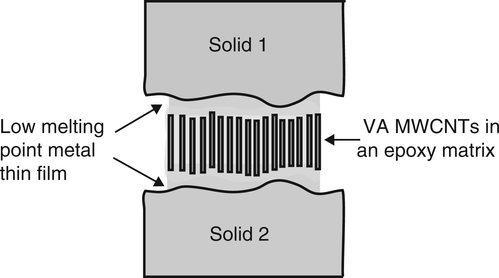
In particular, in the present study we obtain the thermal conductivity of the Sn-coated VA-MWCNT epoxy composite (device) over a temperature range 240–300 K using the three omega method. In order to estimate the thermal conductivity of the VA MWCNT epoxy composite as well as the thermal interfacial resistance at the various material interfaces in the cross-plane direction, we characterize the thermal conductivity in individual constituents of the VA-MWCNT composite, namely (1) individual free-standing nanotubes selected from the same VA-MWCNT array as that used in the fabrication of the VA-MWCNT-epoxy composite; (2) the epoxy matrix; and (3) Sn thin films (capping layer) of ∼500 nm thickness. A 1-D multilayer thermal model based on Feldman’s notation 36 is developed and used in conjunction with the measurements to estimate the thermal conductivity of the CNT-epoxy composite as well as the thermal interfacial resistance between the material layers.
The organization of the paper is as follows: First, a brief description on the processing of the VA-MWCNT composite samples is provide; this is followed by the methods employed in the characterization of thermal transport in its individual constituents, and finally the results and discussion of the study are presented.
Materials and methods
Sample processing
The VA-MWCNT arrays used (Figure 2(a) and (b)) in the present investigation were procured from the laboratory of Prof Shanov at the University of Cincinnati. The CNT arrays were synthesized using water-assisted chemical vapor deposition (CVD).37–39 The nanotube diameter varied from 15 to 45 nm.
Scanning electron microscope (SEM) micrographs of vertically aligned multiwalled carbon nanotube (VA-MWCNT) arrays prepared by thermal chemical vapor deposition (CVD) taken at two different magnifications (a) ×740 and (b) ×6200 showing the region near CNT tips.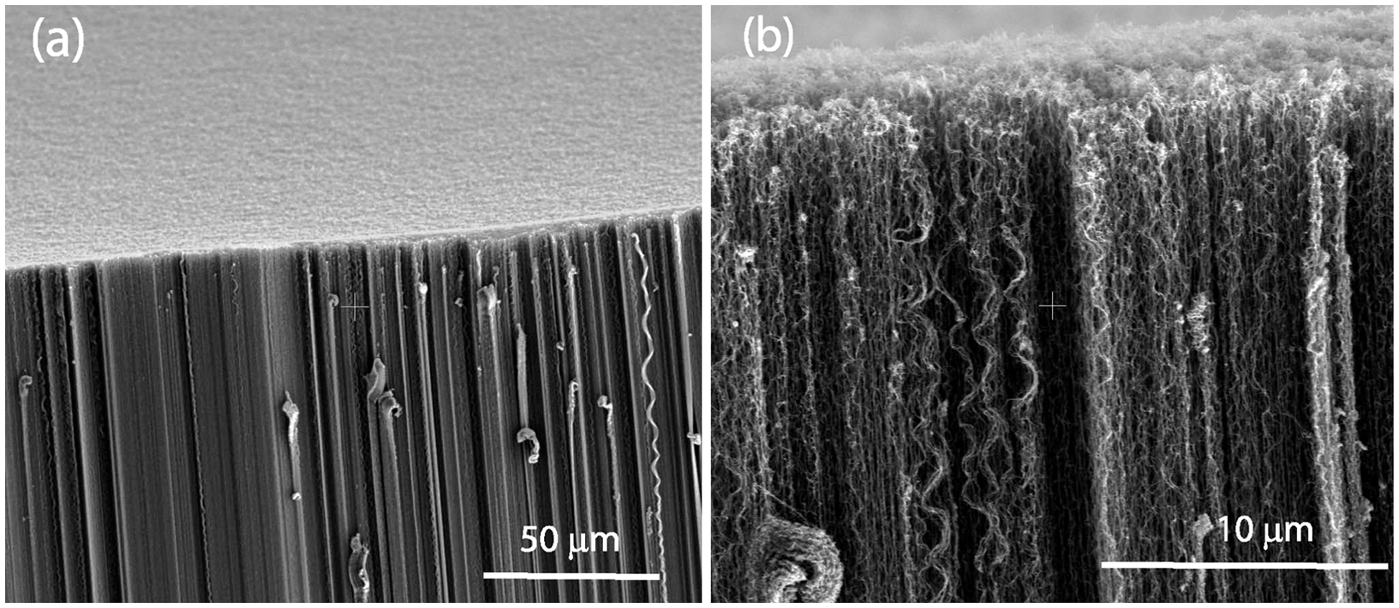
The Epon 862 resin has been chosen due to its higher working temperature which is important for aerospace applications and low viscosity so that it infiltrates the array and provides sufficient adhesion with the embedded CNTs. Moreover, the resin is known to impart good stiffness and toughness, as well as excellent chemical, electrical and thermal resistance, making it a promising matrix for advanced multifunctional composites.40,41 For example, carbon-filler composites with EPON-862 as matrix 41 have been shown to exhibit enhanced flexural and compression modulus and strength and high glass-transition temperatures.
The epoxy-based CNT composites were fabricated by immersing the MWCNT array into a solution of Epon 862 epoxy, EPICURE curing agent W, and an acetone solvent. Prior to immersion of the VA-MWCNT array, the Epon 862 epoxy is ultrasonicated for approximately 8 min. The solution is poured onto the VA-MWCNT array and then spin-coated to allow the epoxy to infiltrate the array. Degassing is performed under high vacuum (30 in of Hg) to remove the bubbles generated during mixing. After casting the MWCNT/epoxy composite, both surfaces are cut and lapped. The surfaces are then sequentially polished at 100–150 rpm with 15, 6, 1, and 0.1 µm diamond abrasives while applying a 5 N constant force.
The sample, as observed under an environmental SEM, mostly comprised of nanotubes having outer diameters 35–45 nm with a number density of ∼109–1010 nanotubes/cm2. Using this information and by measuring the sample dimensions, the estimated average volume fraction of CNTs in the composite is estimated to be approximately 8%. This value is also supported by the weight measurements of VACNT arrays from the same batch in air using density of air of 1.2 kg/m3, and an average density of VACNT array samples of approximately 0.05 g/cm3. Moreover, the amount of polymer infiltration is estimated by comparing the measured density of a composite sample to the density predicted for the case in which the polymer had fully infiltrated the space between the nanotubes. In the present study, polymer infiltration is estimated to be 60–65% of the available spacing.
Atomic force microscopy (AFM) topology measurements (Figure 3(d)–(f)) indicate that the polishing process reduces the roughness of the samples from nearly 1 µm to 100 nm or less. Following polishing, the samples are ethanol-washed and air-dried. The MWCNT tips are exposed from the epoxy by reactive ion etching (RIE) using O2 plasma with 13.5 MHz 125 W RF power for 6–8 min. Once the tips are exposed, a thin layer of tin of thickness ∼500 ± 50 nm is deposited using RF sputtering at 2 × 10⁻⁷ Torr. Besides promoting the transport of phonons from the CNTs to the tin film, the relatively soft tin layer helps in reducing the roughness (and/or gaps) between the CNT tips and the SiO2 layer, thus reducing the thermal interface resistance at the CNT-SiO2 interface.
(a) Atomic force microscopy (AFM) phase imaging of vertically aligned multiwalled carbon nanotube (MWCNT)–epoxy composite before plasma-etching; (b) tapping mode AFM reveals CNT tips exposed after plasma-etching on composite; (c) three-dimensional (3D) view of roughness characteristic on top surface of epoxy before polishing using AFM; (d) surface topology of epoxy composite before polishing indicating roughness 600 nm–1 µm; (e) surface topology traced by AFM tip on composite sample after polishing indicating roughness of the order ∼100 nm.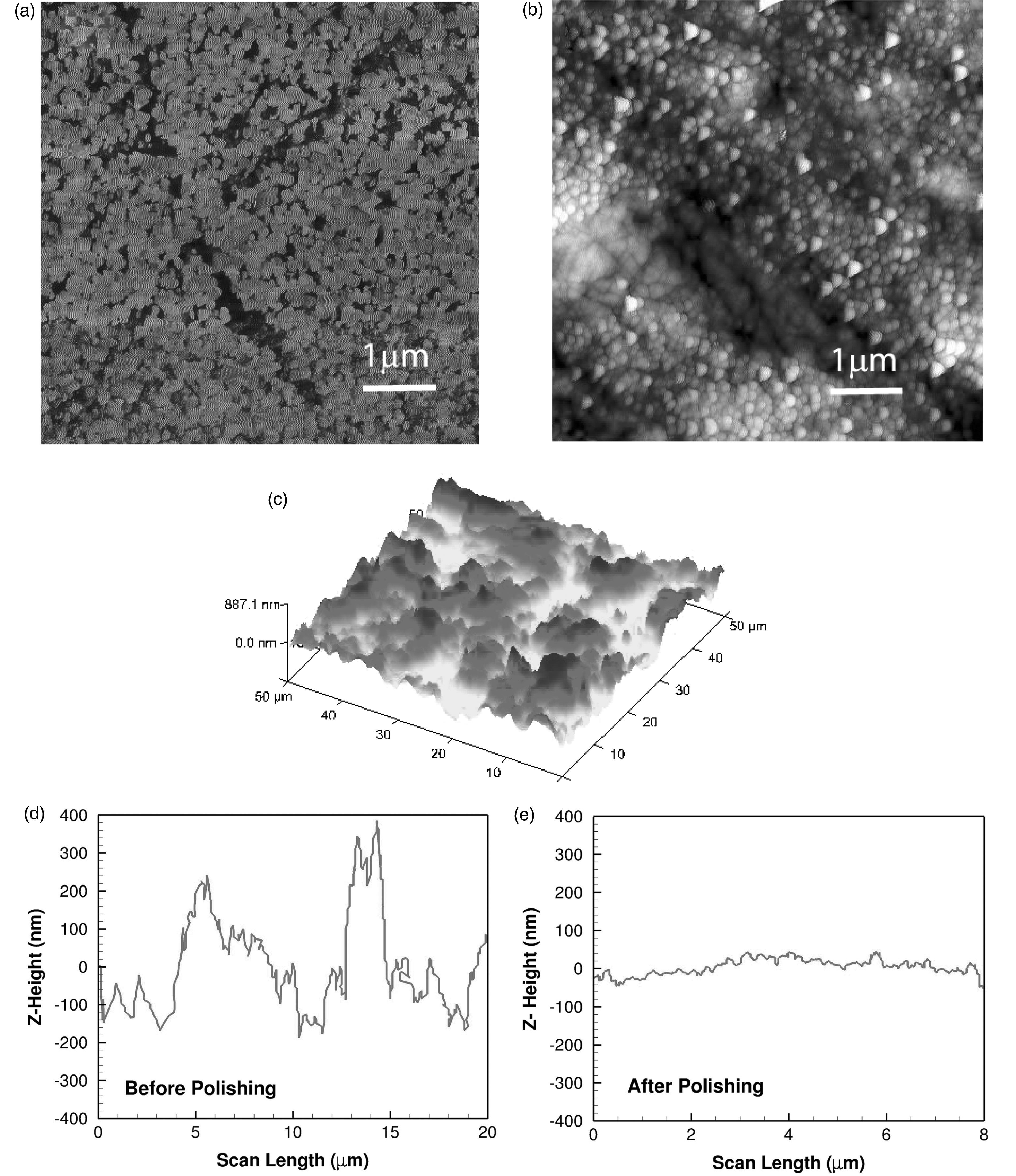
Thermal conductivity measurements in individual MWCNTs
In the present study, the thermal conductivity of individual MWCNTs is measured using a three-omega-based Wollaston T-Type probe inside a high-resolution scanning electron microscope (SEM). Details of the technique and measurements are provided in Bifano et al.
42
Figure 4 depicts the Wollaston probe wire’s temperature profile (a) before the specimen is placed in contact and (b) following contact with the specimen. The drop in spatially averaged temperature causes a reduction in electrical resistance, and thus a measureable voltage decrease. The thermal resistance of the probe wire is then determined from the voltage response since the heating current amplitude is known.
Schematic of the Wollaston probe wire. The probe wire is Joule-heated with a power of Q
RMS
, by the low frequency current, I1ωRMS. θ
A
(x) is the temperature response of the probe wire prior to making contact with the sample of unknown thermal conductivity. Following contact with the sample, the temperature response of the probe wire is θ
B
(x). The measured third harmonic voltage, V3ωRMS, is a function of the probe wire’s thermal resistance, zero current electrical resistance R
eo
, Q
RMS
, and the thermal resistance of the sample. The sample’s thermal conductivity is determined by measuring the sample’s thermal resistance and dimensions.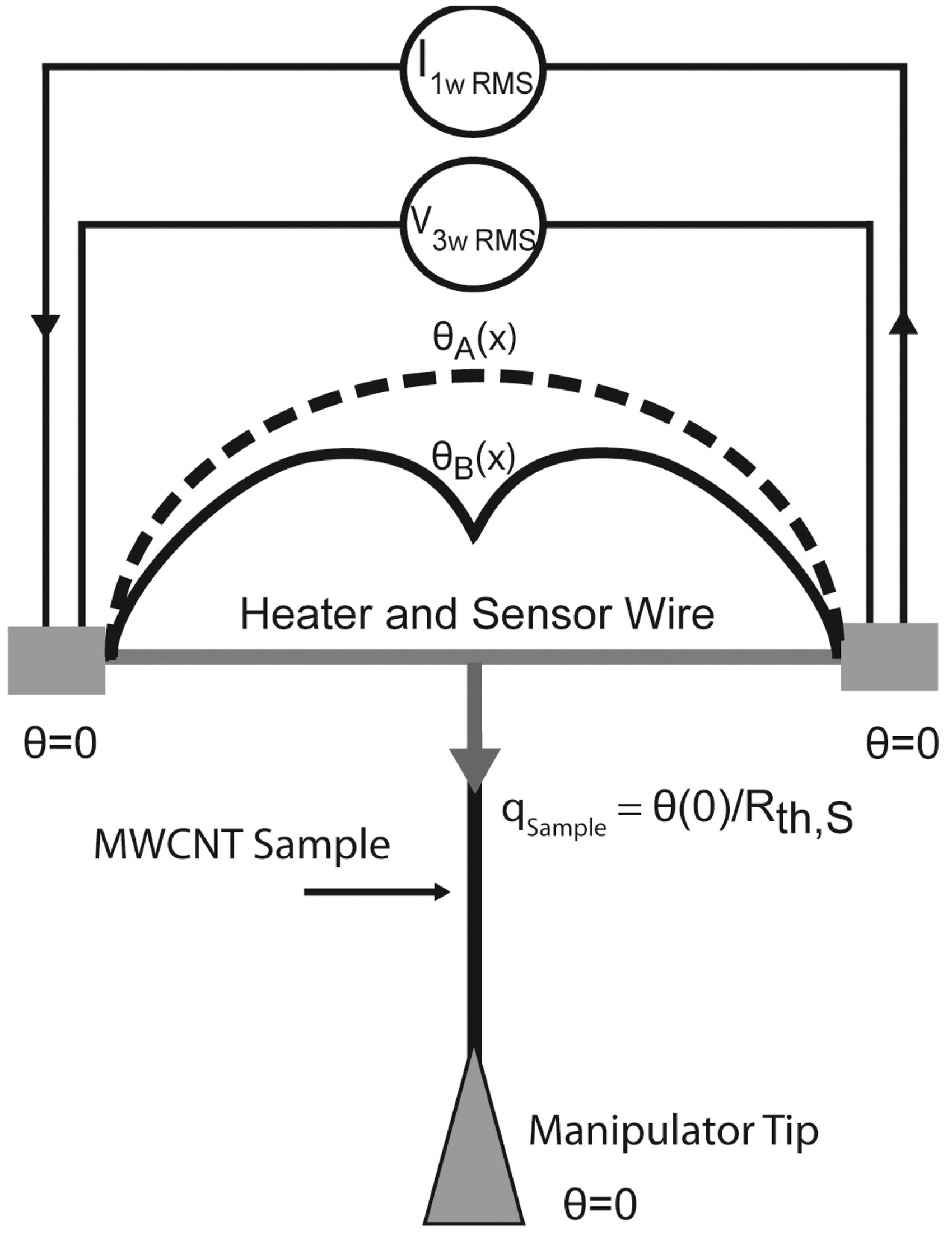
In the method, the relationship between the probe wire’s temperature and its electrical resistivity is first calibrated by measuring the electrical resistance versus power input in the absence of the sample. Once the sample is attached to the probe/heater wire, the change in the measured electrical resistance versus power input of the probe wire is correlated to the decrease in the probe wire’s average temperature rise due to heat flux into the sample. Since the opposing ends of the sample is maintained at the base (ambient) temperature, in effect, the temperature drop and heat flux into the sample can be estimated, and the sample’s thermal resistance determined with sufficient accuracy.
Instead of DC Joule heating and voltage measurements, the probe wire is Joule-heated with a low frequency sinusoidal AC current, I(t) = I1ωsin(ωt), where I1ω is the current amplitude. The initial electrical resistance of the probe wire is R
eo
. Joule heating at 2ω, Q(t), drives in phase temperature oscillations,

A Lock-in amplifier is used to measure the specific RMS value of the three-omega component. The measurable 3ω RMS voltage response from equation (2) may be re-written as

If Re3ω,RMS ≡ V3ω,RMS/I1ω,RMS, Zo is determined from the measured slope of
The three omega for thermal conductivity measurements in Sn thin films, bulk epoxy and MWCNT-epoxy composite
In the present study, an approach similar to the differential three-omega method43–45 was utilized to measure the thermal conductivity of a ∼500 nm thick Sn film, bulk EPON-862 epoxy, and VA-MWCNT-epoxy composite samples. In general, the 3ω method is performed on these samples by passing a current with angular frequency ω through a heater/sensor microfabricated on the sample surface, as shown in Figure 5(c) and (d). The current leads to Joule heating and thus a temperature oscillation at a frequency 2ω in the heater/sensor wire. Subsequently, the metal heater/sensor wire’s electrical resistance also oscillates at 2ω causing a measureable 3ω voltage oscillation detected using a lock-in amplifier. The 3ω voltage measurements are then used to determine the sample’s thermal properties.46,47 The frequency range for the experiments is chosen by examining the relationship between the film (sample) thickness, the thermal penetration depth of interest, and the heater width. Large heater widths (when compared to sample thickness) produce a one-dimensional heating profile, thereby providing information about the cross-plane thermal conductivity.
The main components for the 3ω set-up (see Figure 5(a)) used in the present work are (1) a cryostat (Janis Research Model: CCS-400H/204); (2) a temperature controller that serves to regulate the sample temperature; and (3) a lock-in amplifier to detect the voltage response of the heater (Figure 5). The cryostat as shown in Figure 5(b) is capable of operating in the temperature range from 10 K to 500 K. An RV-8 rotary vane pump capable of developing a vacuum of 10−4 torr or less is utilized. A silicon shadow mask is batch fabricated using the conventional lithography technique. Using this microfabricated shadow mask an aluminum metal heater/sensor line is magnetron sputtered on the sample surface. The temperature coefficient of resistance of the heater/sensor line is measured prior to every experiment. The set-up has been automated using LabVIEW 8.5. The bits of the multiplying DAC (AD 7541 KN) are set ‘on’ and ‘off’ to balance the first harmonic signals from the sample and reference resistor. Moreover, the LabVIEW program helps in balancing the first harmonic voltage at the reference resistor and the sample resistor to a greater degree of precision and subsequently extract third harmonic voltage signals in order to determine the temperature rise in the heater/sensor.
(a) Schematic of Cryostat Setup@ Nanomechanics Lab, Case Western; (b) microfabricated 25-µm wide heater with 250 µm × 250 µm pads attached for wire-bonding; (c) schematic of the conventional 3-Omega set-up used in measurement of the cross-plane thermal conductivity of the samples using the thin film on a substrate configuration (refer corresponding scanning electron microscope [SEM] images, Figure 7).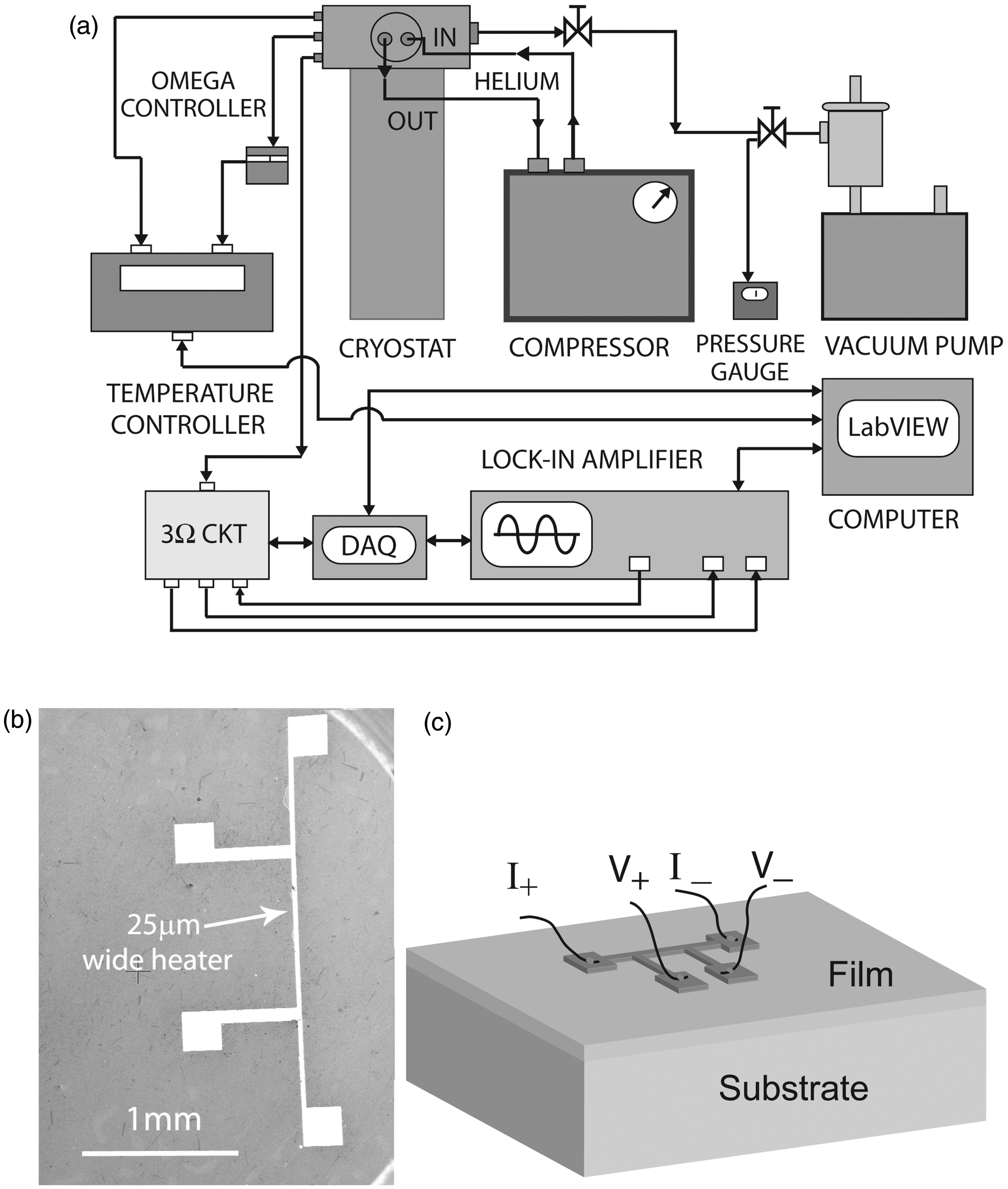
For electrically conductive samples, a thin insulating film must be deposited prior to the metal line deposition to provide electrical isolation. In the present work, approximately 350 nm thick SiO2 films were deposited using a low temperature plasma enhanced chemical vapor deposition (PECVD) process. The SiO2 layer serves as an insulator for all thin films and composite samples evaluated in the present study. Moreover, in all cases, the same heater material (aluminum) and heater dimensions (width) are used. In order to minimize errors due to various approximations of the exact thermal solution for the case of a thin film on a substrate, a numerical procedure in conjunction with the exact solution, as described by Kim, 48 Borca-Tasciuc et al., 43 and more recently by Tong, 45 is employed. The analysis of the three omega experiments was based on the work by Cahill and Pohl 49 and requires the assumption that the heater wire is of infinite length and that the sample dimensions be semi-infinite. Additionally, the method requires the heat penetration depth into the sample to be greater than the heater width, thus satisfying the approximation of an infinite line heat source. Additional details about the three omega technique can be found from various references43–49 and are therefore not discussed in detail here.
In the present study, the aforementioned three omega method was employed to investigate the thermal conductivity of a 3-mm thick epoxy (EPON-862) sample using the analytical solution discussed in Cahill 46 for a narrow line source on a semi-infinite substrate. On the other hand, the thermal conductivity of ∼500 nm thin tin films was measured by comparing the total amplitude and phase signal of temperature oscillations with a theoretically obtained solution in the thin layer limit using Tong’s 45 two-layer model. For the case of the VA-MWCNT composites, a three-layer model based on Feldman’s algorithm 36 was derived and used to interpret the experimental results.
Results and discussion
In the present study, we present results of thermal conductivity measurements in individual components of the VA MWCNT epoxy composites including individual free-standing MWCNTs, epoxy matrix, and the tin capping layer. Wherever possible, the thermal measurements were performed at room and lower than room temperatures so as to investigate the effects of increased phonon mean free path lengths on thermal conductivity.
Thermal conductivity in individual carbon nanotube
In the present study, thermal conductivity of individual MWCNTs taken from the same sample batch array UC01 are measured at room temperature. The average thermal conductivity of an individual nanotube from the UC01 batch was found to be ∼60 W/m-K based on the slope change in measured third harmonic resistance versus power input to sensor with and without sample (Figure 6(c) and using equation 3). In a recent study,
42
the authors’ have also measured the thermal conductivity of individual multiwalled nanotubes from both heat-treated and non-heat-treated sample groups, showing an approximate five-fold increase in thermal conductivity with heat treatment. Heat-treatment was performed at 3000°C for 20 h in an argon gas atmosphere. Moreover, for one of the heat-treated samples, thermal conductivity as high as 730 ± 153 W/m-K was obtained.
(a) Scanning electron microscope (SEM) micrograph of thermal conductivity experiment on an individual multiwalled carbon nanotube (MWCNT) selected from the UC01 sample group. (b) Raman intensity with excitation wave number for D/G Raman ratio of the UC01 nonheat-treated sample. (c) Measured third harmonic resistance vs power input to sensor with and without sample for an individual nanotube (UC sample).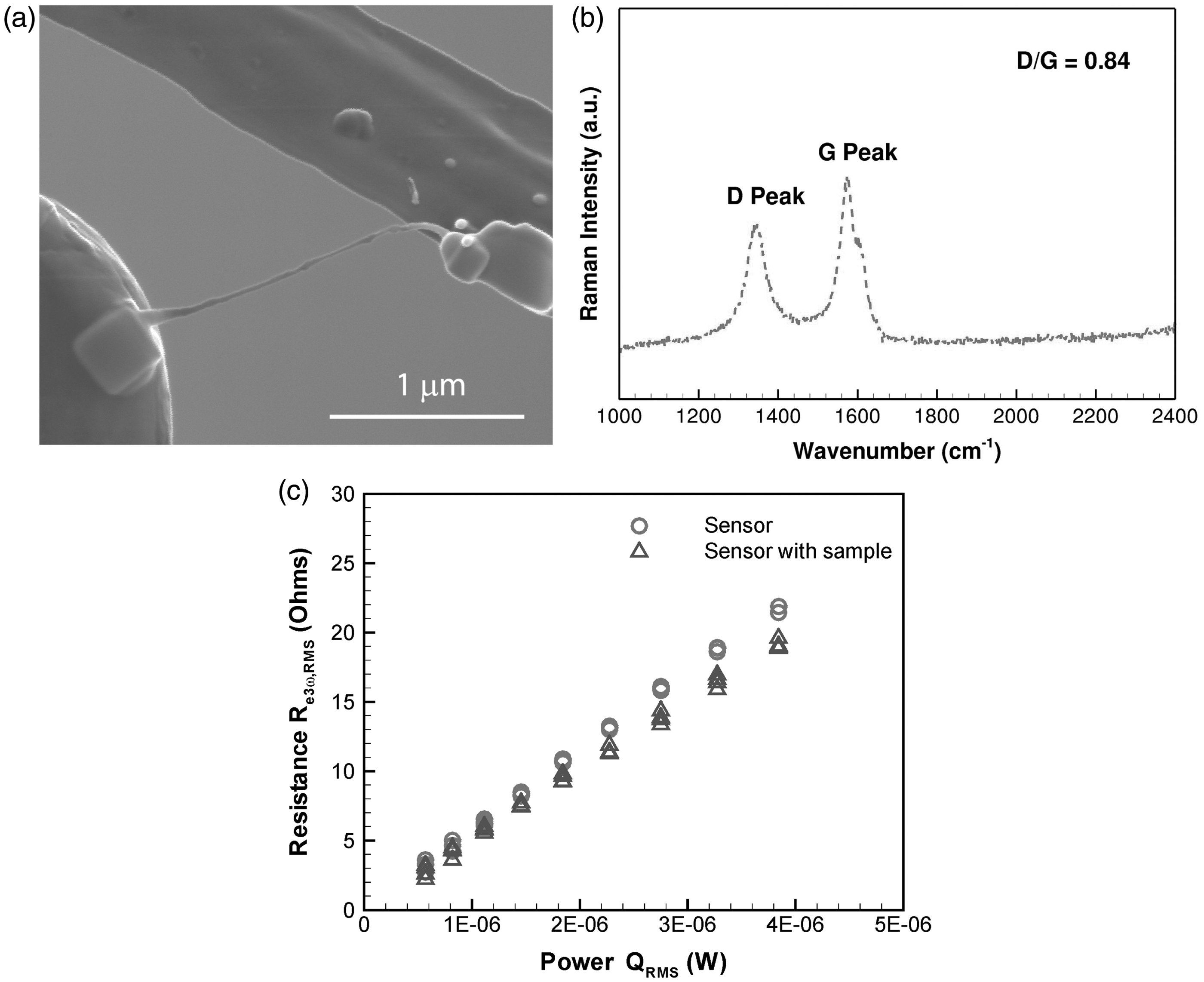
Qualitative assessments of residual amorphous carbon and defects were made by observing the Raman peak intensities of the D and G-bands. The D band (defect band) is known to be activated by both carbonaceous impurities with sp3 bonding and fragmented sp2 bonds,50,51 both being features of MWCNT defects. The G band is activated by contiguous sp2 bonding, i.e., a high degree of crystallinity.50,51 Therefore, when comparing the two sample groups, a smaller D/G band ratio is representative of a sample with fewer defects and a higher degree of graphitization. The authors have shown that significant increase in thermal conductivity had a strong correlation to the reduced D/G Raman peaks. The average Raman D/G ratio for heat-treated samples was 0.21 ± 0.04, while the non-heat-treated group had an average D/G ratio equal to 0.69 ± 0.15. Note that the UC01 samples are not heat-treated and Raman scattering reveals a D/G ratio of 0.84 (Figure 6(b)). The reduced value of thermal conductivity measured in the UC01 sample correlates well with the non-heat-treated sample group with higher D/G Raman ratios.
Thermal conductivity is undoubtedly expected to improve with increased crystallinity and a decreased density of phonon scattering sites. Andrews et al. (2001) 52 had observed marked structural and chemical improvements in MWCNT sample quality with heat-treatment. It was observed that annealing temperatures reduced the residual Fe catalyst (essential for CVD growth of MWCNT’s) from 7.1% by wt. to 0.1%. Moreover, it was reported that the temperatures as high as 3000°C healed the sidewall defects evident from the reduced inter-layer spacing between grapheme shells confirmed by x-ray diffraction (XRD) and transmission electron microscope (TEM).
Thermal transport in 500 nm thick Sn thin film
In the present study, a TZ (capping layer) comprising of a Sn thin film is introduced at the interface between the MWCNTs and the bounding surfaces to minimize scattering of the phonons at the interface due to mismatch in phonon spectra as well as thermal interface resistance due to interfacial roughness including the effects not all CNTs making contact at the interface due to unequal length of CNTs. The Sn capping layer, with a relatively high thermal conductivity and low yield strength (46 W/m-K and melting point of 230°C), aids in filling the surface asperities at the two mating surfaces, thereby reducing the interface thermal resistance between the CNT-epoxy composite and the bounding surfaces. Considering diffuse interfaces, even in the regions where the Sn layer wets the CNT tips completely (no air gaps), phonons from the CNT tips are expected to be readily transferred to the Sn layer because of the relatively wide phonon spectrum available to the phonons in Sn when compared to the CNTs (phonon spectra in a material is proportional to the density of states, which is proportional to the inverse of the cube of the sound speed in the material). Additionally, the capping layer is kept relatively thin to help minimize the boundary layer thickness and hence its thermal resistance. As previously mentioned, the top surface of the composite is polished down to ∼100 nm, as verified by AFM. Therefore, a 500-nm thick tin layer should be sufficient to fill the asperities. The thin layer of tin is deposited on the composite sample using sputtering. The sample is then placed in a vacuum oven at near melting point of tin so that it forms a weld contact with the exposed CNT tips on the top surface. Recent work by Prasher 53 has confirmed that the weld contact formed by Sn-like soft (and compliant) metals tend to increase the thermal conductance by an order of magnitude compared to more common Van der Waal contacts at the interfaces.
In order to obtain the cross-plane thermal conductivity of the Sn thin film specimens, the differential three-omega method was applied with the Sn thin film specimens deposited on a Si substrate. The Sn film is assumed to be thin enough such that one-dimensional Fourier conduction model can be applied for the analysis and interpretation of the experimental data. Specific conditions that must hold to ensure accurate analysis are given by Scanning electron microscope (SEM) images of heater/sensor wire deposited using shadow mask on (a) SiO2 350 nm thin film and Sn 500 nm thin film (with an insulating layer) on silicon substrate. Experimental parameters for thin film measurement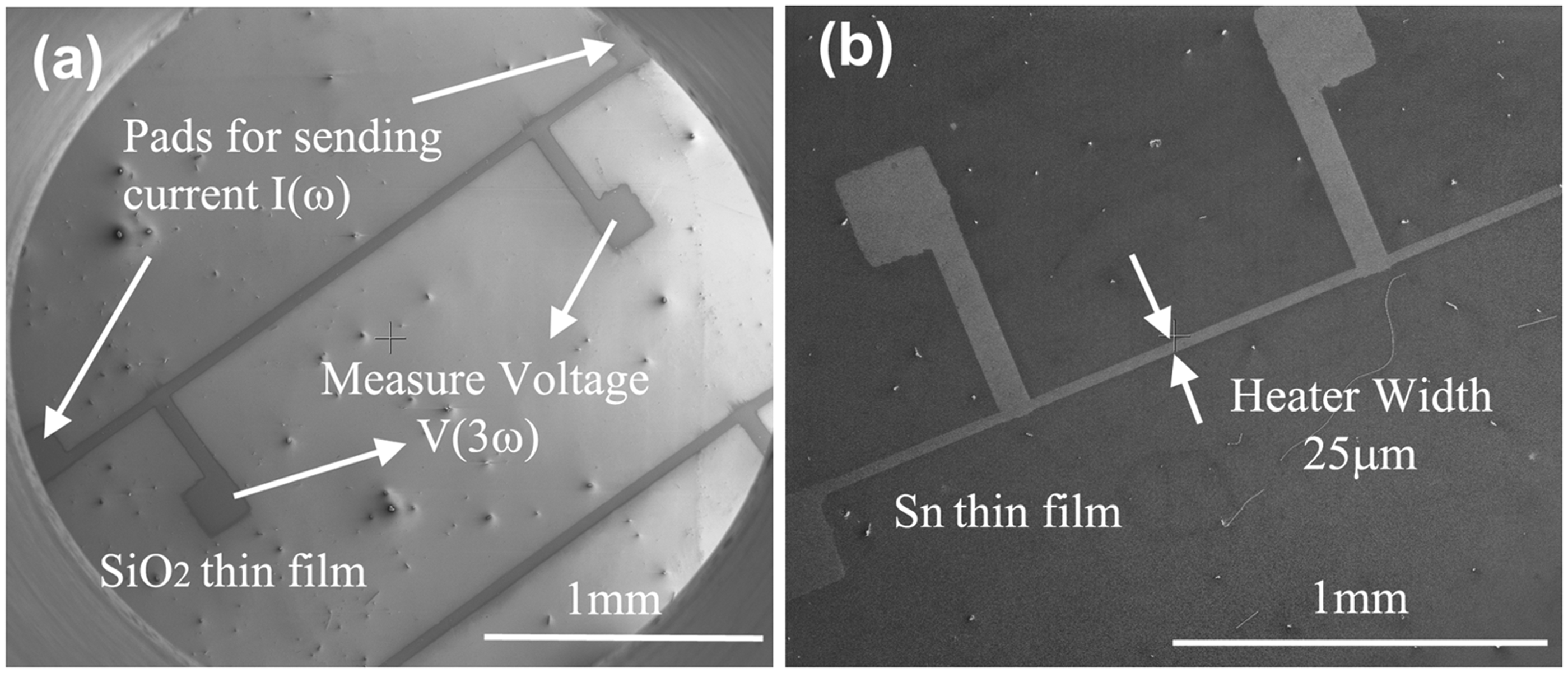

From these experiments, 54 the thermal conductivity of the 500 ± 50 nm tin film was determined to be 46 ± 4 W/m-K at room temperature. The thermal conductivity was found to remain nearly constant in the temperature range of 240 K–300 K (Figure 8). This is understood to be due to the specific heat being constant in the temperature range with the Dulong-Petit limit being at 210 K. Moreover, the phonon and electron mean free paths at room temperature are relatively small, 50 nm and <5 nm, respectively, compared to the boundary dimensions. 54 Therefore, boundary scattering is not expected to play a role in the thermal conductivity of the sample. Furthermore, even though the reduction in thermal conductivity in metals is known to occur at elevated temperatures due to the increased phonon-phonon inelastic scattering, the test temperatures in our present case are not high enough for inelastic phonon-phonon (Umklapp) interactions to be important, and thermal conduction continues to be dominated by the specific heat. The estimated thermal resistance of the Sn thin film over the measured temperature range is nearly constant at 1.09 × 10⁻⁸ K-m2/W.
Thermal transport in epoxy polymer
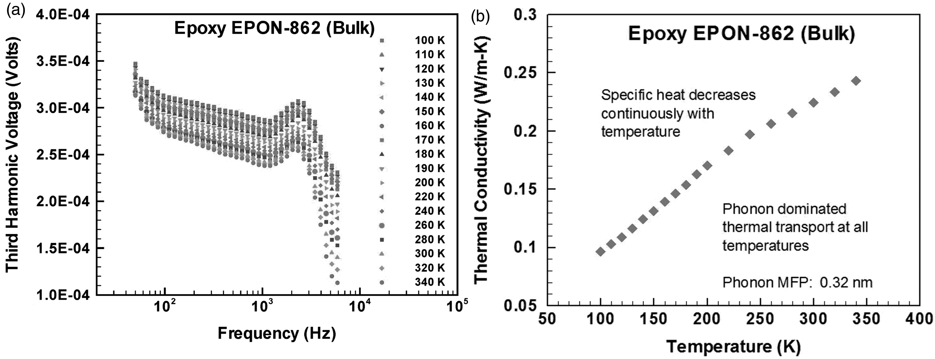
The thermal conductivity of EPON-862 epoxy is also measured using the three-omega method at temperatures in the range 100 K to 340 K (Figure 9). The measured thermal conductivity of EPON-862 at room temperature is 0.224 ± 0.02 W/m-K. The slight increase in thermal conductivity with temperature is understood to be a result of the increase in specific heat with test temperature. The thermal transport in amorphous polymers (Reese
55
) is phonon-dominated with the mean free path of phonons remaining a constant due to scattering by the amorphous disordered regions. For the case of EPON-862, the phonon mean free path is estimated to be 0.32 nm based on the sound velocity (dilatational wave velocity) of 1949 m/s (corresponding to the elastic modulus value of 2.58 GPa
41
and Poisson’s ratio of 0.35) and specific heat equal to 1060 J/Kg-K.
56
The glass transition temperature of EPON-862 is 408 K,
41
and the thermal conductivity of Epon-862 is expected to increase continuously until it reaches the transition point. A small jog in the temperature dependence of thermal conductivity is observed at around 225 K, which is consistent with the observations made earlier in many polymers for specific heat dependency with temperature, and can be attributed to the transition of the local amorphous regions within the polymer from glassy to the rubbery state. The rotational and vibrational motions of atomic groups associated with the polymer chains in the rubbery state require a lesser amount of energy for reorganization and mobility when compared to the glassy state.
Thermal conductivity of 500 nm Sn thin film (Replotted from Reference [54]). (a) Third harmonic voltage measurements vs frequency for epoxy EPON-862 (bulk) at different temperatures; (b) thermal conductivity vs temperature of epoxy EPON-862 from 100 K–340 K.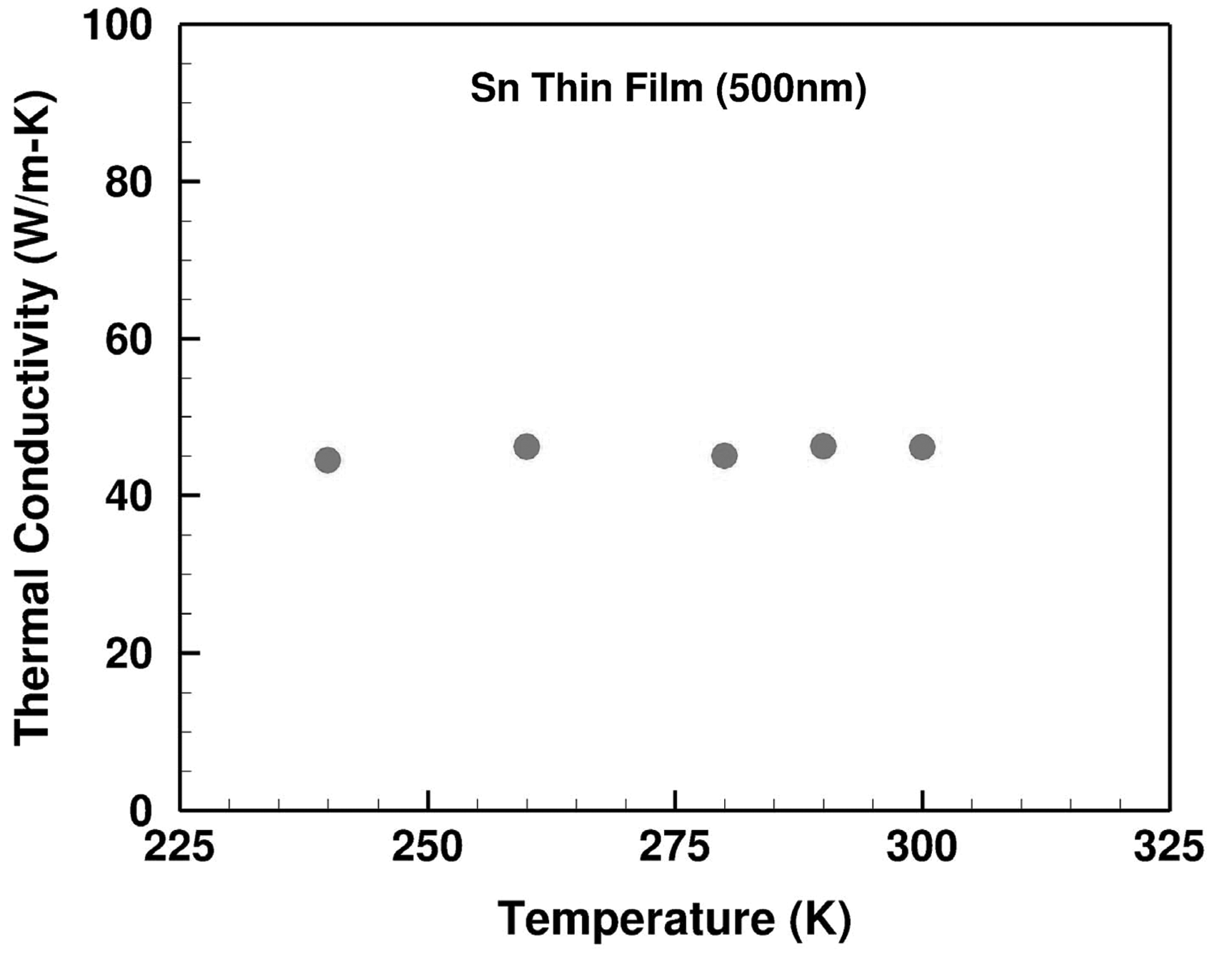
Thermal transport in the vertically aligned MWCNT–epoxy composite
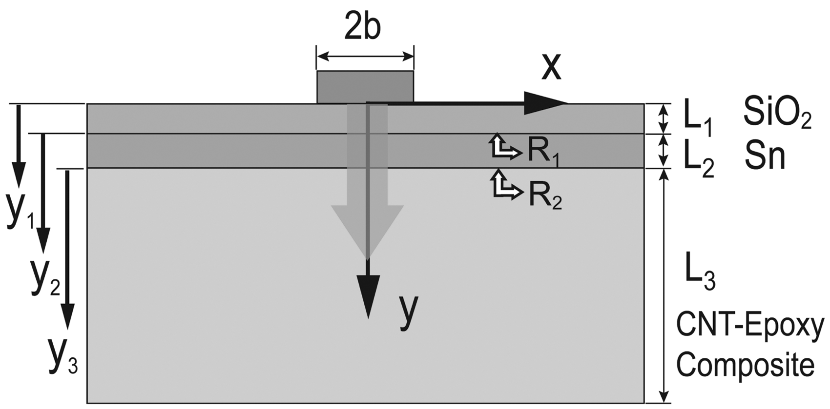
In order to characterize the thermal conductivity of the VA MWCNT-epoxy composite, the three-omega method outlined earlier is employed. A thin layer (∼500 nm) of tin with a SiO2 insulating layer on top is deposited on the composite substrate (Figure 10) to prevent direct contact with the aluminum heater line and contact pads. The estimation of both thermal conductivity and thermal interface resistance between the layers is important to obtain the through-thickness thermal conductivity of the VA MWCNT-epoxy composite. Tong in an earlier work
45
derived a two-layer model (based on Feldman’s notation
36
). A three-layer 1-D model including the finite interface resistance between layers has been derived in this work (Figure 11).
Scanning electron microscope (SEM) images of (a) cross-section of multiwalled carbon nanotube (MWCNT) array; (b) cross-section of vertically aligned MWCNT array composite from one of its edges in backscattering mode, on a 45° sample holder with 35° tilt; (c) line heater deposited on top of MWCNTA–composite sample; (d) top cross-section of the measured sample after slicing showing SiO2–Sn interface and Sn–MWCNT composite interface; (e) bottom cross-section showing vertically aligned multiwalled carbon nanotube (VA-MWCNT) array on silicon wafer; and (f) schematic of 3-omega configuration utilized for measuring VA-MWCNT composite. Schematic representation of one-dimensional (1D) thermal transport model for a three-layered structure with a heater on top.
The main steps of the 1-D thermal-model are provided below. The heat equation for a 1-D multilayer problem can be written as,

Under periodic excitation with angular time frequency, ω, the general solution to equation (4) can be expressed as


Let us assume for this 1-D material, a periodic heat flux with amplitude q0 and frequency ω is injected at the surface y1 = 0

Following Feldman’s notation,
36
we can express the temperature at any position y as a vector,
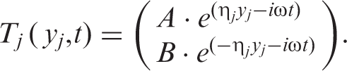
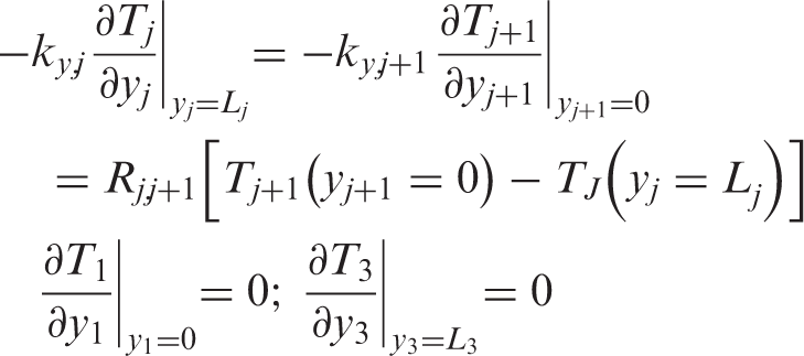
The matrix formulation aids in finding the correlation between the temperatures at two different locations within the medium as well as that across the interface between the layers. The boundary condition is based on the assumption that with no heat generated or absorbed at the interfaces, the heat flux is continuous across the interfaces, and there is discontinuity in temperature across a j and j+1 interface due to a finite interface thermal resistance R
j
,j+1
.
The total thermal impedance Z of the three-layered structure neglecting the interface thermal resistance can be obtained as

Similarly, the total thermal impedance Z for the three-layered structure with interface resistances R1 = R1,2 (between SiO2 and Sn) and R2 = R2,3 (between Sn and MWCNT) can be expressed as

The model is verified by comparing them with the results obtained for the two-layer model as described by Tong.
45
Moreover, using the condition, 
The experimental data on temperature oscillations and phase are compared with the predictions of the thermal model with and without thermal interface resistance between the layers. The thermal model is based on several parameters (shown in Table 2), e.g., thermal properties of the various layers, and the unknown thermal interface resistances. An iterative algorithm, as described in Tong et al.,
31
was employed to obtain the best fit values for the unknowns. The comparison of the experimental results and model predictions based on the best fit values for the unknown parameters is shown in Figure 12. From these comparisons, the thermal conductivity of the CNT-epoxy composite is estimated to be 5.8 ± 0.64 W/m-K at room temperature. The measured amplitude as well as the phase of the temperature oscillations are found to be sensitive to the thermal conductivities of tin, MWCNT-epoxy composite, and the thermal interface resistances. A ±20% uncertainty in thermal conductivity of either tin or the MWCNT-epoxy composite results in a corresponding ±5–10% shift in the amplitude of the temperature oscillations from the measured values. The thermal conductivity of the composite exhibits a slight increase with temperature between 240 K and 300 K (Figure 13) and is understood to be dominated by the specific heat dependence with temperature of the Epon-862 epoxy.9,57
Comparison of thermal model with and without interface resistances with experimental data: (a) temperature oscillations vs frequency and (b) phase of oscillations vs frequency. Thermal conductivity vs temperature of vertically aligned multiwalled carbon nanotube (VA-MWCNTA)–epoxy (EPON-862) nanocomposite from 240 K–300 K. Model parameters that fit the experimental amplitude and phase of temperature oscillations VA-MWCNT: vertically aligned multiwalled carbon nanotube.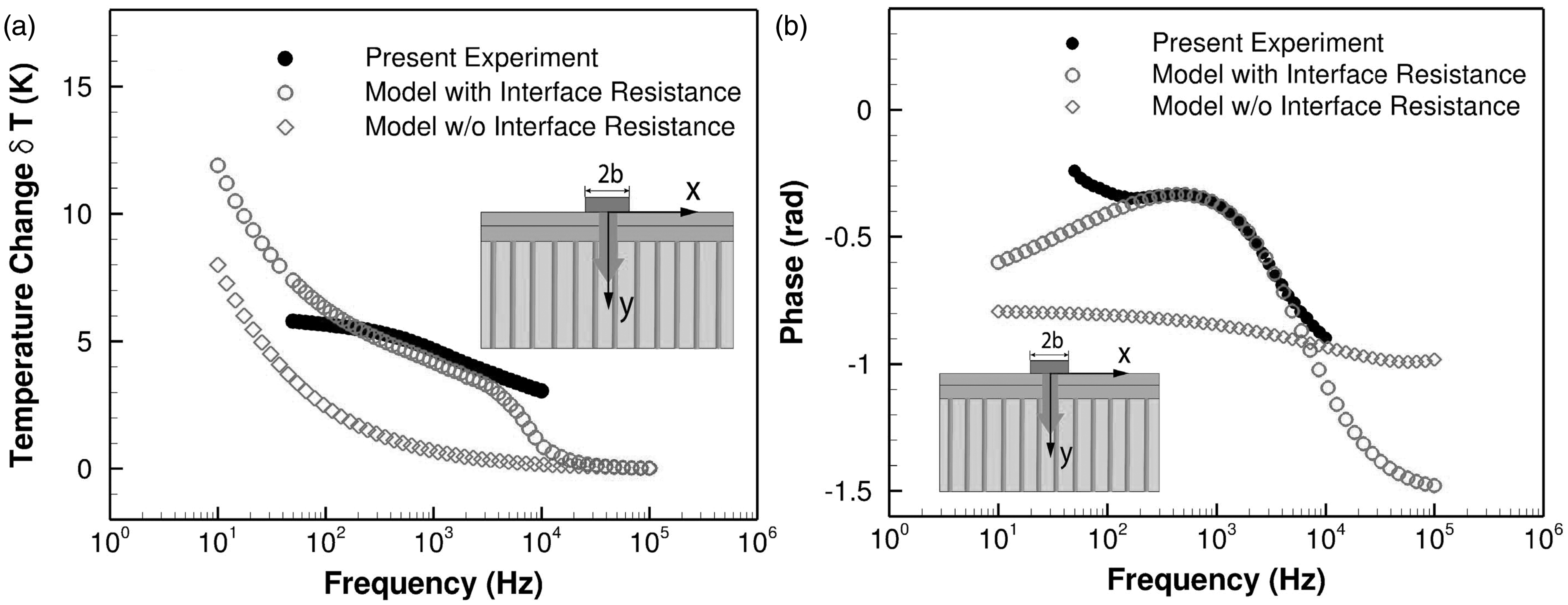
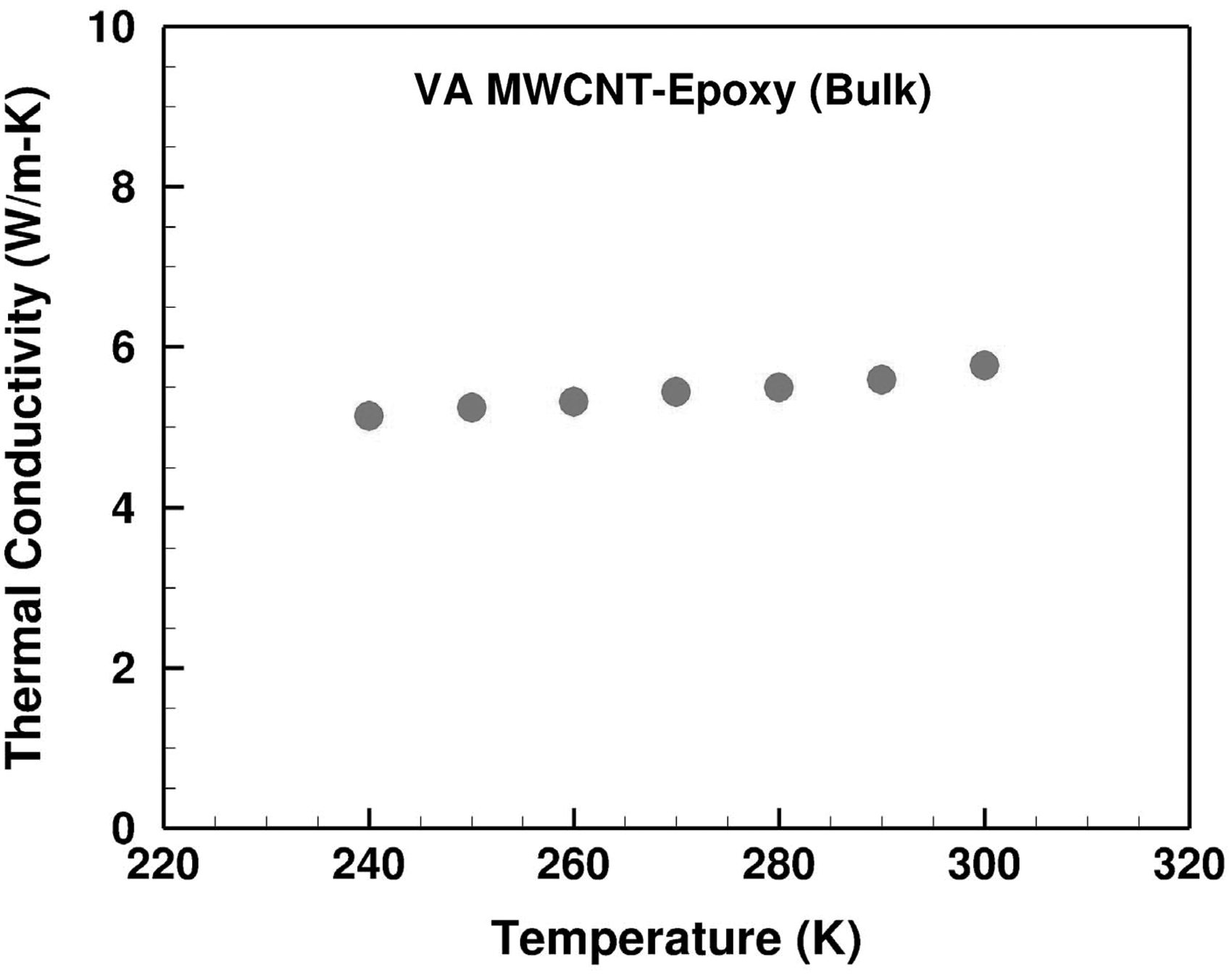

The best fit estimates for the interface thermal resistances R1-2 (between SiO2 and Sn) and R2-3 (between Sn and MWCNT) are 5 × 10⁻⁵ m2-K/W and 8 × 10⁻⁶ − 8.5 × 10⁻⁷ m2-K/W, respectively. The amplitude or phase of temperature oscillations is especially sensitive to the thermal resistance of the rougher interface, i.e. the SiO2–Sn interface. However, it is relatively less sensitive to the interface thermal resistance of the relatively smooth Sn-MWCNT interface, and therefore by keeping all other parameters constant we can estimate the interface resistance of the smooth Sn-MWCNT interface to within an order of magnitude range. The interface resistance between the layers is a combination of Kapitza resistance based on diffuse mismatch model (DMM) and constriction resistance at the contacts of CNTs with the Sn layer. Recently, Prasher58,59 suggested that for nanosized constrictions (which the vertically aligned MWCNTs make with the layer above it), the effects of mismatch in acoustic properties are more dominant than due to constriction of the heat flux lines. Therefore, vibrational spectra mismatch between Sn, a soft metal with relatively low sound speed, and VA MWCNTs is expected to restrict the thermal conductance through the MWCNT composite. The Debye temperature of Sn is 170 K, while the Debye temperature for multi-MWCNTs is much higher, 960–2500 K, indicating a large mismatch in vibrational spectra of the two materials. Interface thermal resistance between two highly dissimilar materials with large differences in phonon spectra, e.g., interfaces involving metal and dielectric solids, as pointed out by Lyeo and Cahill 60 is not only due to the coupling of electrons in a metal and phonons in a dielectric substrate but also by anharmonic processes (namely three-phonon processes) that can contribute a significant additional channel for transport of heat by altering (increasing) the phonon frequency by inelastic scattering processes. These higher frequency phonons are expected to be readily accommodated by the much broader phonon spectra available for Sn. For these reasons, CNTs may be particularly attractive for exchange of thermal energy with Sn across the CNT-Sn interfaces involving both phonons and electrons.
Interestingly, even after a spate of research on VA MWCNT composites, there are only few published works in the literature that reported thermal conductivities greater than 1 W/m-K (Figure 14). Sihn et al.
32
have reported the highest thermal conductivity so far for a 30 µm VA MWCNT-epoxy composite. Using a simple 1-D thermal resistance network model, we estimate the room temperature thermal conductivity of their VA MWCNT-epoxy composite to be 137 W/m-K. Considering a 10 vol % of MWCNTs in their composite, the thermal conductivity of individual MWCNTs is estimated to be in excess of 1000 W/m-K.
Thermal conductivity vs volume fraction of nanowires and nanotubes.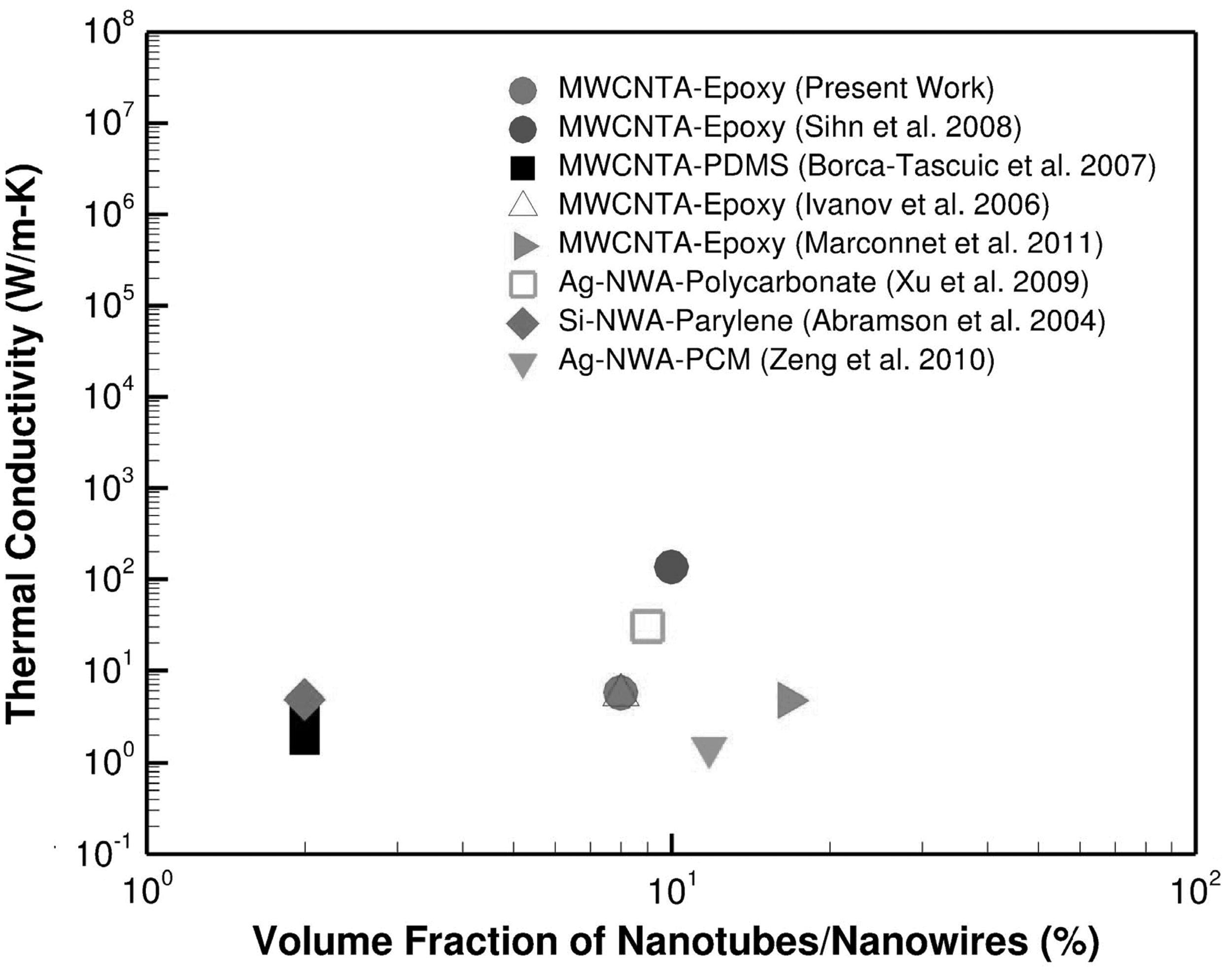
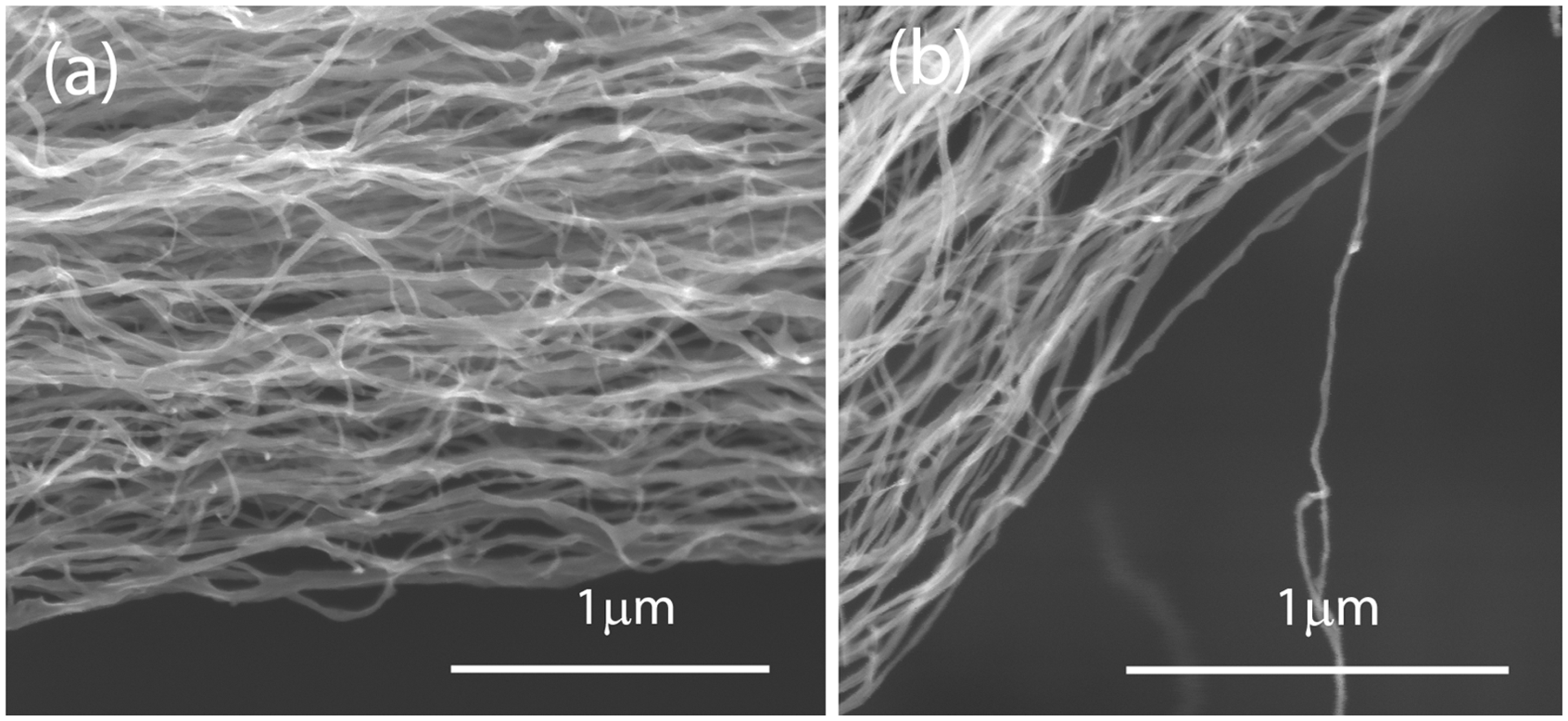
The primary reasons for a less than 1 W/m-K thermal conductivity of the MWCNT polymer composites reported in the literature may be due to the low volume fraction of CNTs used in the composites as well as their defect state and purity. In a parallel study, 42 the authors investigated thermal conductivity in annealed and as-received thermal CVD grown individual multi-MWCNTs. They reported a five-fold increase in thermal conductivity of the MWCNTs from the annealed batch (Figure 15), conforming that the defect state of the CNTs play an important role in controlling the thermal conductivity in individual CNTs. In addition, high-resolution SEM micrographs of CNT arrays (Figure 16) from the same batch as the array that was used in the fabrication of the composite indicate physical deformities, including entanglement of CNTs and fused contacts, that are understood to be the reason for reduced thermal conductivity of the composites. These contact regions between nanotubes occur even in the best-aligned CNT films and serve as scattering sites for phonons propagating along contacting nanotubes. In fact Prasher et al. 61 have shown that the thermal conductivity of a randomly oriented bed of MWCNTs is primarily controlled by the CNT-CNT thermal contact resistance, which is an order of magnitude larger than the intrinsic thermal resistance of a CNT.
Another reason for the relatively low thermal conductivity of the individual CNTs may be because the phonon modes within CNTs can be damped and scattered by the polymer matrix reducing the thermal conductivity of the CNTs themselves. Indeed, Gojny et al.
17
have shown that damping of phonon modes within the outer shells of the nanotube may be a possible reason for the reduction of the thermal conductivity of the nanotubes.
Thermal conductivity vs Raman ratio of individual multiwalled nanotubes (replotted from Reference [42]). Scanning electron microscope (SEM) micrographs (9 kV, 3.5 mm working distance, and spot size, 2.5) of multiwalled carbon nanotube (MWCNT) array batch of which the composite was made and tested: (a) entanglements of individual nanotubes (×87,000) and (b) individual samples are often attached as if they are fused together (×100,000).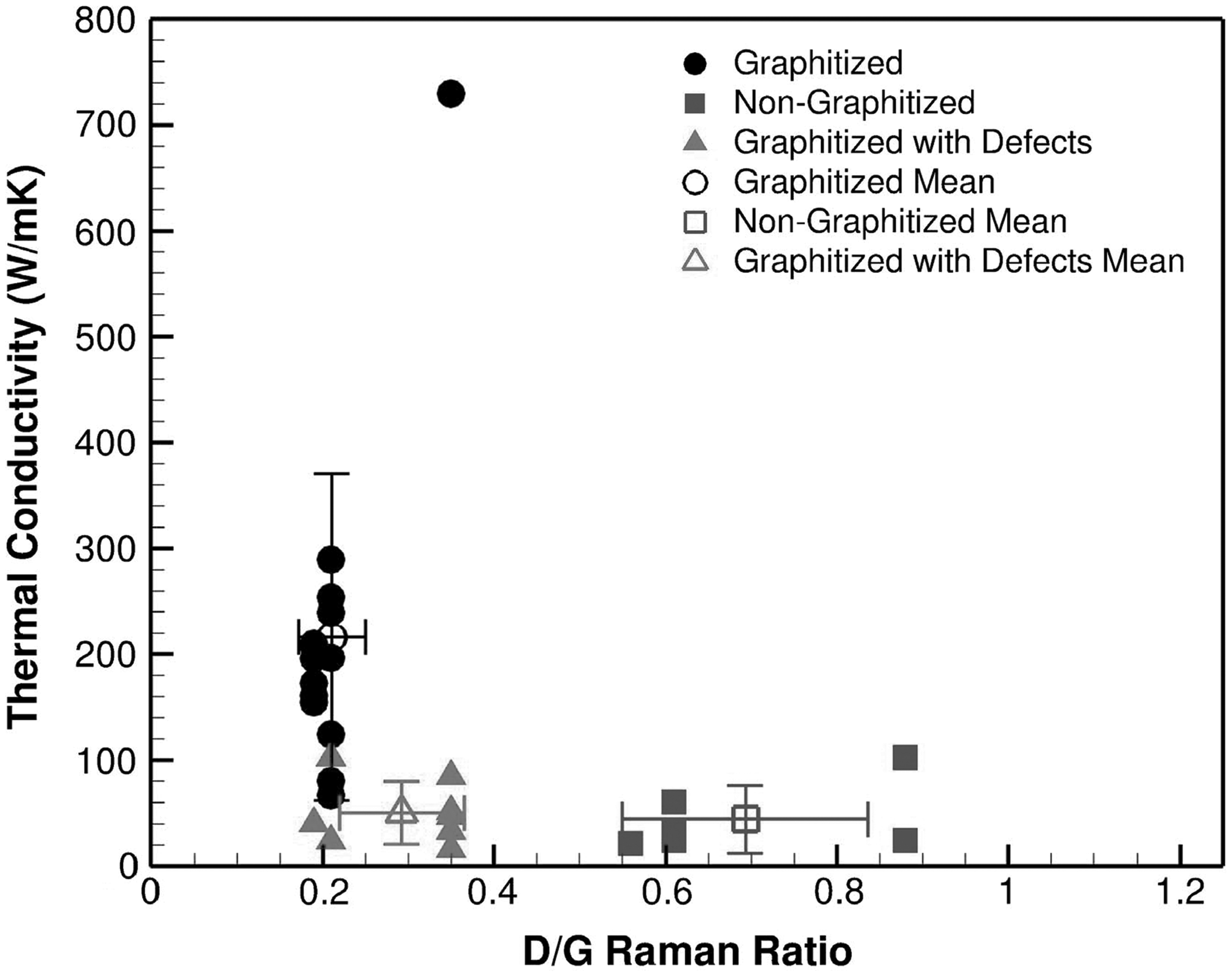
Additionally, in order to improve their performance as TIM, thermal conductance at CNT-capping layer interfaces need to be addressed. One of the main advantages of the composites studied in this work is that CNTs themselves are well aligned and span the entire thickness of the polymer in the axial direction, providing direct pathways for heat transport across the composite. However, if some CNTs fail to extend to the surface of the polymer, the CNT-polymer thermal boundary resistance can negatively impact the axial conduction. In this regard, in the present study we initially start with a polished CNT-polymer surface and then plasma-etch it to expose the CNT tips on the surface. These tips are then coated with a low-yield point (Sn) metal to fill the region in between the CNT tips. The results of the present study suggest that the thermal interface resistance for such relatively smooth CNT-metal interfaces may contribute to only second-order effects in the thermal performance of the TIMs at room temperature.
It is to be noted that most previous works reported in the literature on VA-MWCNT-polymer composites21,22,32,62 show room-temperature thermal conductivity as high as metal nanowire array-polymer composites63,64 and the semiconductor nanowire array-polymer composites65,66 with nanowire volume fractions in the same range as the CNTs. Nevertheless, the five-fold increase in thermal conductivity in the post-annealed MWCNTs suggests that the thermal conductivity of VA-MWCNT-epoxy composites can be designed to be as high as 25 W/m-K, which can potentially have a major impact in the design of multifunctional, load-bearing, high-thermal performance structural interfaces for a variety of thermal-management applications.
Summary
This paper reports development of VA-MWCNT array composites for thermal energy management in load-bearing structural applications. Unlike previous studies on the characterization of VA-MWCNT-based TIMs for primarily non-load bearing applications, the material systems of interest here involve the use of VA MWCNTs in an epoxy matrix. The epoxy matrix imparts mechanical strength to these systems while the VACNTs provide avenues for high through-thickness thermal conductivity across a typical material interface. In order to obtain the thermal characteristics of these multifunctional TIMs, we report measurements of thermal conductivity in the Sn-capped VA-MWCNT-epoxy composites as well as in its individual constituents, i.e., bulk EPON-862 (matrix material) and Sn thin film, in the temperature range 240 K to 300 K, and individual multiwall CNTs at room temperature taken from the same VA-MWCNT batch as the one used to fabricate the CNT-epoxy TIM. The thermal conductivity of the epoxy and Sn thin film was obtained as a function of temperature by using a cryostat in conjunction with the three-omega method. The thermal conductivity of individual free-standing MWCNT samples was obtained by employing the Wollaston T-type three-omega probe method inside a high-resolution SEM equipped with nanomanipulators and a gas injection system for electron beam-induced platinum deposition. The thermal conductivity of bulk EPON-862 epoxy was observed to increase gradually from 0.1 W/m-K at 100 K to 0.24 W/m-K at 340 K and is understood to be dominated by the heat capacity of the epoxy. The thermal conductivity of Sn capping layer (500 micron film thickness) was observed to remain nearly constant at about 46 W/m-K over the above-mentioned temperature range. The thermal conductivity of individual free-standing CNTs was measured to be about 60 W/m-K at room temperature. A 1-D multilayer thermal model that includes effects of thermal interface resistance and the thermal conductivity of the CNT-epoxy composite and its constituents was used to interpret the experimental results. The thermal conductivity of the CNT-epoxy composite was estimated to be about 5.8 W/m-K and exhibits a slight increase with temperature in the range of 240 K to 300 K. The best fit estimates for the interface thermal resistances between SiO2 and Sn and between Sn and MWCNT were 5 × 10⁻⁵ m2-K/W and 8 × 10⁻⁶ − 8.5 × 10⁻⁷ m2-K/W, respectively. The results of this study suggest that the inclusion of an Sn thin layer on the VA-MWCNT array as well as the morphological structure of the individual MWCNTs are dominating factors that control the overall thermal conductivity of the TIM. These results are encouraging in light of the fact that the thermal conductivity of a VA-MWCNT array can be increased by an order of magnitude by using a standard high-temperature post-annealing step. In this way, multifunctional (load bearing) TIMs with effective through-thickness thermal conductivities as high as 25 W/m-K can be potentially fabricated.
Footnotes
Funding
This research received no specific grant from any funding agency in the public, commercial, or not-for-profit sectors.
Acknowledgments
The authors would like to acknowledge the support of the Air Force Office of Scientific Research (AFOSR) grant FA9550-08-1-0372 (Program manager Dr. Byung-Lip Lee) and the National Science Foundation Major Research Instrumentation grants CMMI-0521364 and CMMI-0922968 to Vikas Prakash.
Conflict of interest
None declared.