






Abstract
Broadband electromagnetic wave absorbers are essential for enhancing the survivability of next-generation stealth platforms operating in multiband radar environments. In this study, a three-dimensional (3D) pixelated honeycomb absorber is designed, optimized, and fabricated to achieve high absorption efficiency at a limited thickness while maintaining an ultralightweight nature and structurally integrable characteristics via direct pixel implementation on honeycomb cell walls. Conductive ink patterns are printed directly onto the aramid honeycomb cell walls according to a pixelated arrangement optimized using a genetic algorithm. The optimized 20-mm-thick structure exhibits a density of approximately 50.6 kg/m3, slightly higher than that of the pristine aramid honeycomb (47.8 kg/m3), confirming that it retains its lightweight nature. Experimental results reveal the structure’s broadband absorption performance, exhibiting a −10 dB reflection loss bandwidth covering a substantial portion of the 1–18 GHz range, despite the single-layer configuration and nonmagnetic composition. A comparative analysis reveals that doubling the thickness to 40 mm while maintaining the same pixel design results in limited performance improvement, underscoring the decisive role of the proposed 3D pixel optimization approach in mitigating the conventional thickness–bandwidth trade-off. The developed absorber design provides structural scalability, manufacturing consistency, and adaptability to various platforms, indicating strong potential for practical applications in composite structures for preparing stealth aircraft air inlets, weapon systems, and unmanned aerial vehicles.
Keywords
Highlights
• Designed and optimized 3D pixelated honeycomb absorber via genetic algorithm. • Printed conductive ink onto aramid honeycomb cell walls for integration. • Achieved broadband −10 dB absorption over the 1–18 GHz range with 20 mm thickness. • Maintained lightweight structure with density close to that of pristine honeycomb. • Overcame the conventional thickness–bandwidth trade-off through pixel optimization.
Introduction
As stealth technology has become a critical factor in determining the survivability of modern military and aerospace platforms, development of structures with limited electromagnetic detectability across various frequency ranges has become essential. Stealth fighter aircrafts, guided munitions, and high-speed unmanned aerial vehicles, which operate in multifrequency environments such as the S-, C-, X-, and Ku-bands, require low-visibility structures capable of responding effectively to threats. However, in conventional absorber designs, a fundamental trade-off exists among high absorption efficiency, broad bandwidth, and reduced thickness, resulting in structural limitations. 1
Conventional electromagnetic wave absorbers are typically based on composite structures incorporating magnetic loss materials2–4 or possessing multilayered Jaumann structures.5–8 These approaches aim to achieve high absorption through the use of magnetic materials or to realize broadband absorption via multilayered designs; however, they often suffer from structural complexity and increased weight. Consequently, the demand for developing new material combinations and structural design strategies to achieve broadband impedance matching, without relying on magnetic materials, is surging. Resonator-based metamaterials,9–15 pixelated metamaterial surfaces,16–21 and multilayered dielectric-coupled structures have been explored to realize electromagnetic wave absorption without the use of magnetic components, leveraging design flexibility and frequency selectivity to increase absorption. Among these, honeycomb-based structures have attracted particular attention as next-generation absorbers, as they simultaneously satisfy lightweight and structural stiffness requirements while increasing electromagnetic absorption bandwidth through multiple reflections and path delay effects.22–24 In addition to these structures, various sandwich-type radar absorbing structures have been investigated to combine electromagnetic absorption capability with structural load-bearing performance. For example, polyurethane-foam-based sandwich absorbers, incorporating conductive fillers, reportedly achieved broadband attenuation across microwave frequency ranges. 25 Similarly, nanocomposite sandwich structures, combining CNT-filled composite face sheets with honeycomb cores, exhibited broadband microwave absorption while maintaining structural stiffness. 26 More recently, multifunctional sandwich absorbers based on lightweight polymer foam cores have been proposed, exhibiting electromagnetic absorption capability along with mechanical load-bearing performance. 27 Furthermore, structural design approaches considering electromagnetic compatibility, such as composite inserts for sandwich radome structures and additive-manufacturing-based multilayer radar absorbing structures, have been explored to improve structural integration and fabrication flexibility.28,29 However, despite these advantages, they still lack sufficient design freedom to achieve broadband performance.
Based on these findings, in this study, we propose a lightweight honeycomb-based structure capable of achieving broadband electromagnetic absorption without magnetic fillers or multilayer stacking. The approach introduces a binary pixel grid onto the internal walls of the aramid honeycomb structure, where each pixel is either filled or left unfilled with a conductive ink and optimized using a genetic algorithm (GA). Unlike conventional planar pixel absorbers, the proposed method implements pixel optimization directly within the three-dimensional (3D) honeycomb architecture, enabling broadband absorption while maintaining a structurally lightweight composite design. This integration of pixel-based optimization with a honeycomb framework enhances impedance matching and frequency selectivity while remaining compatible with scalable roll-to-roll fabrication. Consequently, the proposed structure demonstrates high potential as a lightweight and structurally integrable electromagnetic absorber for aerospace composite applications.
Design and optimization
Design concept of the pixelated honeycomb absorber
Pixelated metasurface structures have been reported to exhibit superior electromagnetic wave absorption across wider frequency ranges than single-resonance absorbers, while simultaneously reducing polarization sensitivity and enabling radar cross-section reduction.17,19
These structures control surface impedance as a function of frequency through discrete pixel-level arrangements. By determining the presence or absence of each pixel (zero or one), they alter current distribution and generate multiple resonance modes, thereby creating several frequency loss paths. Consequently, unlike single-resonator absorbers, they can provide effective reflection loss over a broad bandwidth.
In this study, a pixelated design concept was applied to the walls of a honeycomb cell structure (which can be structurally extended), thereby simplifying fabrication while achieving electromagnetic properties comparable to those of multilayered structures. The cell size of the aramid honeycomb core was 1/8 in, sufficiently smaller than the effective wavelength of the Ku-band, allowing the entire structure to be approximated as an effective medium. Generally, when the wavelength of an electromagnetic wave exceeds periodicity and unit cell size, periodic composite structures behave like continuous dielectric media, and the effective medium approximation can be applied to define their effective permittivity and permeability. Pendry et al. 30 theoretically demonstrated that when the cell size a was significantly smaller than the wavelength λ (a << λ), the structure could be interpreted as an equivalent medium without diffraction effects arising from its internal geometry. Smith et al. 31 experimentally confirmed that such periodic structures behaved as continuous media in terms of electromagnetic wave scattering. Accordingly, the open-honeycomb structure in this study was designed under the assumption that it could be approximated as an effective dielectric medium.
The walls of the honeycomb cells were discretized into pixel units with a resolution of 0.5 mm × 0.5 mm, and the presence or absence of a conductive ink was defined as a binary value (one or zero). This binary array offers significant design flexibility, enabling precise control of the conductive surface impedance in response to incident electromagnetic waves. The structure was designed to achieve ultrawideband electromagnetic wave absorption from the S- to the Ku-bands while remaining lightweight and avoiding the use of magnetic materials or multilayer stacking (Figure 1). Design concept and modeling process for pixelated honeycomb unit cell. (a) Conversion from decimal to binary, (b) assignment of 0/1 to 0.5 mm × 0.5 mm, (c) mapping of the pattern onto honeycomb walls, and (d) construction of the complete unit cell.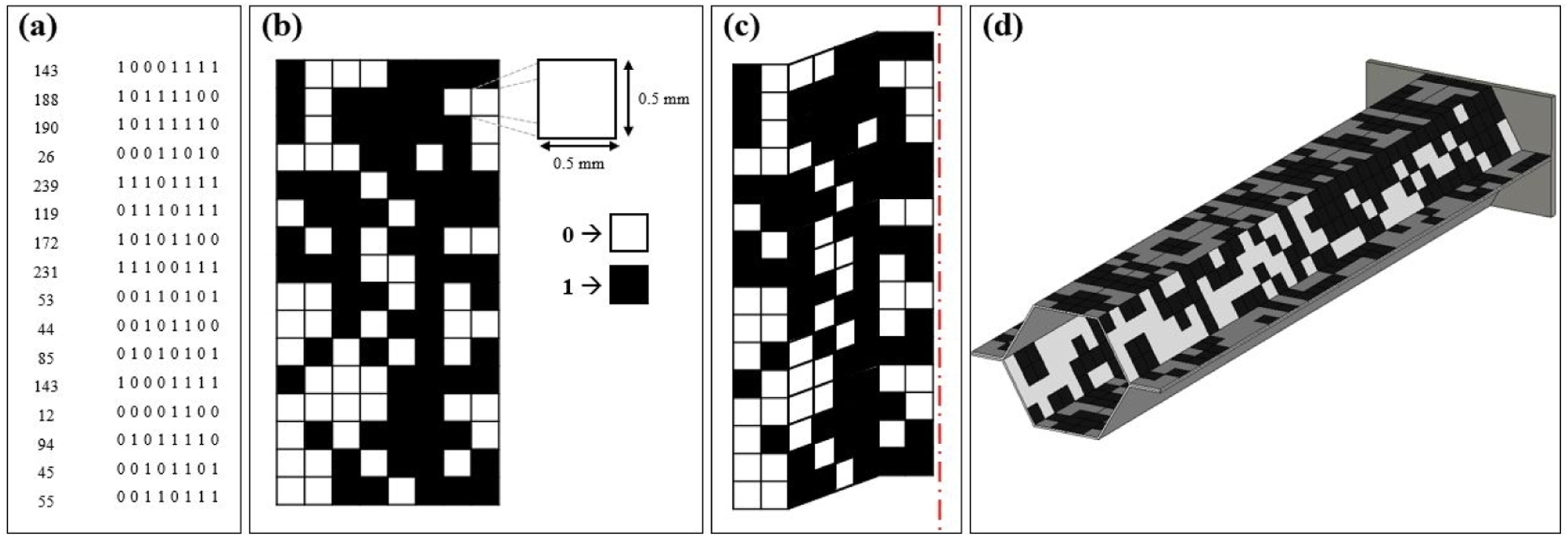
Furthermore, the proposed pixel pattern was implemented as a 3D conductive array structure, which, unlike conventional planar pixel configurations, offers structural flexibility and expanded design freedom along the spatial axis. This 3D binary-array approach enables more precise impedance control under varying electromagnetic wave incidence conditions and can serve as a scalable design platform for optimized configurations tailored to diverse geometries and performance requirements in the future.
GA-based optimization
To minimize reflection loss and achieve broadband absorption using the proposed pixelated honeycomb structure, the pixel pattern on each cell wall was optimized using a GA (Figure 2). The conductive ink used in this study had a surface resistance of approximately 220–280 Ω/sq, and the relative permittivity of the aramid paper was set to ε' = 2.7 with a loss tangent of tan δ = 0.0037. The GA implemented in MATLAB was linked to CST Studio Suite simulations, with the objective function defined to maximize the frequency bandwidth over which the reflection loss S11 remained less than or equal to −10 dB across multiple frequency points. The pixel structure was treated as a design space composed of binary variables, with the initial population generated randomly and then evolved through selection, crossover, and mutation operations. Each individual was evaluated for the reflection loss in the 0.5–20 GHz range using CST simulations. The objective function incorporated weighting factors based on both frequency band and reflection loss, from which the fitness values were calculated. To reduce polarization sensitivity and enhance design generality, the reflection losses under HH and VV polarization conditions were simulated for each candidate, and their average value was defined as the final fitness. This ensured polarization-independent absorption characteristics at the early design stage. GA-based optimization workflow and CST simulation setup.
In this study, the structure length was set to 20 mm for a single module to balance computational efficiency and structural repeatability, and optimization was performed based on this configuration. This length was chosen to simplify fabrication, facilitate pattern alignment during manufacturing, and provide a basic unit suitable for repetitive extension. To evaluate the expandability of the unit structure, a 40-mm configuration comprising two serially repeated 20-mm structures was analyzed for comparison (Figure 3). In this case, both structures shared the same pixel pattern, differing only in the total length, to investigate the changes in electromagnetic interaction due to structural expansion. The optimized pixel pattern was designed to be insensitive to specific polarizations, ensuring consistent absorption across a wide frequency range utilizing multiple resonant frequencies. This approach demonstrates that ultrawideband electromagnetic wave absorption can be achieved with a lightweight single-layer structure, avoiding complex multilayer designs by combining the high design freedom of the pixelated structure with the global search capability of the GA. (a) Pixelated pattern printing and (b) modeling of honeycomb with patterned surface.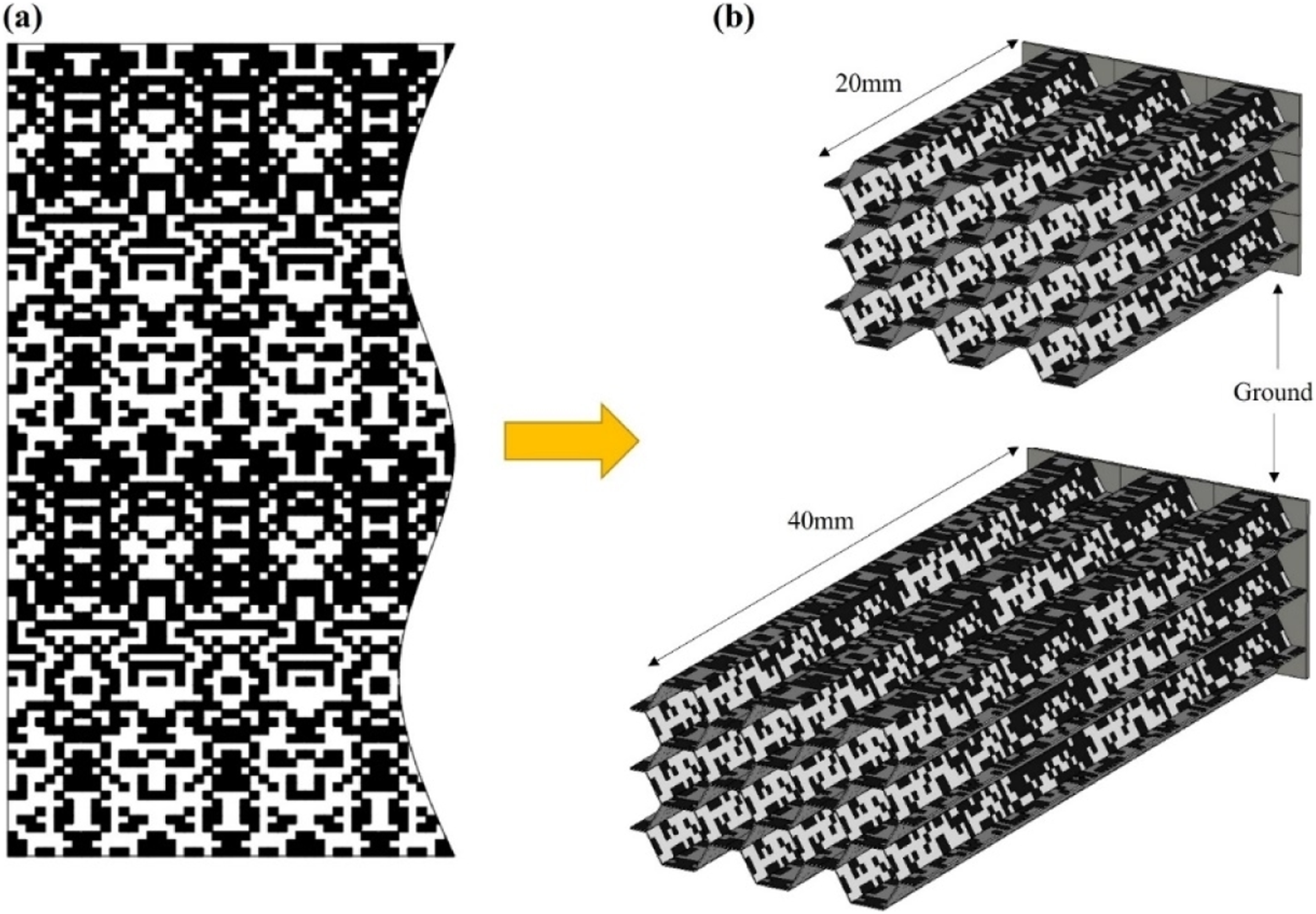
Optimized design results
Figure 4 presents the GA-based optimization process and the corresponding results. Figure 4(a) shows the convergence trend of the cost values during optimization, and Figure 4(b) presents the objective function, with darker colors representing lower cost values, indicating gradual convergence toward optimal solutions over successive generations. To maximize broadband absorption, a greater weight was assigned to the low-frequency region, as securing performance at lower frequencies is critical for expanding the overall bandwidth. Optimization was carried out on a single 20-mm-thick cell using a time-domain solver of CST Studio Suite under periodic boundary conditions and port settings. Figure 4(c) illustrates the intermediate result, which exhibits relatively poor reflection loss and absorption bandwidth characteristics compared with the final optimized result shown in Figure 4(d). By contrast, the final pattern exhibits consistent reflection loss under both HH and VV polarization conditions, with multiple resonance frequencies and a reflection loss below −10 dB across a broad range from approximately 2.5 to 20 GHz. These results indicate that despite being a single-layer nonmagnetic structure, it can achieve broadband absorption comparable to those of multilayer resonance-based designs using a pixelated design. (a) Cost vs iteration, (b) object function, (c) intermediate iteration result, and (d) final optimized result.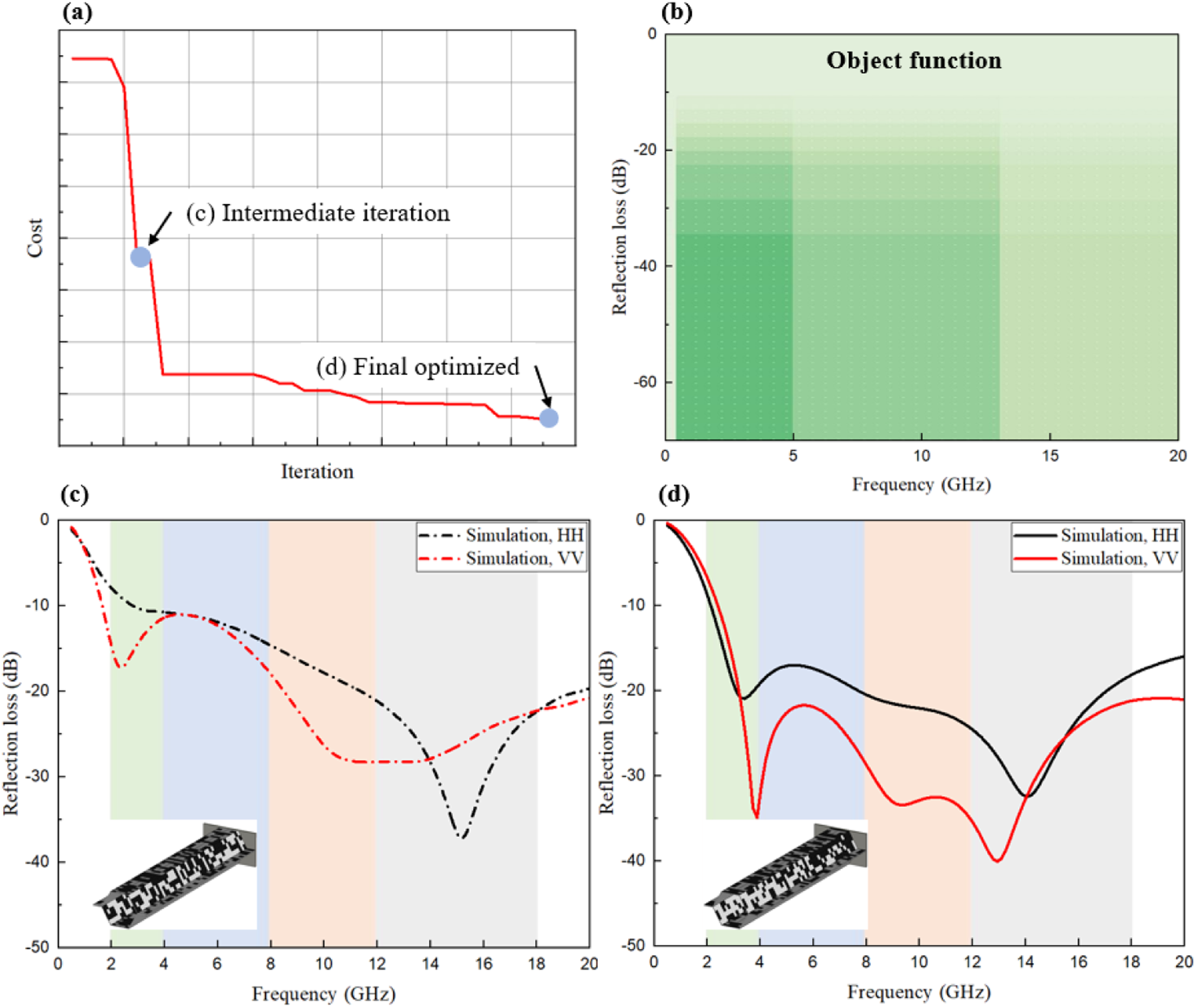
Fabrication and measurement
Several fabrication steps were required to produce an optimized pixelated honeycomb structure. The fabrication process included (1) printing conductive ink patterns, (2) sheet cutting and honeycomb stacking, (3) honeycomb expansion and epoxy resin dipping followed by curing, and (4) specimen machining. The epoxy resin was primarily used to maintain the extended honeycomb geometry and provide structural stability during fabrication. The conductive ink patterns were printed on a 0.05-mm aramid paper using a thermally curable carbon-based ink via a continuous roll-to-roll method. The printing equipment incorporated an inline drying unit, enabling immediate drying and precise control of the ink thickness. A critical design constraint was the minimum printable resolution of the conductive ink, which was less than approximately 0.4 mm in width; therefore, the pixel size was set to 0.5 mm × 0.5 mm. The specimens were machined to a 300 mm × 300 mm configuration suitable for the Naval Research Laboratory (NRL) arch method (Figure 5), ensuring sufficient area to avoid measurement interference and to maintain planar wave conditions during testing. Absorber specimens with 20- and 40-mm thicknesses and the corresponding pixelated patterns.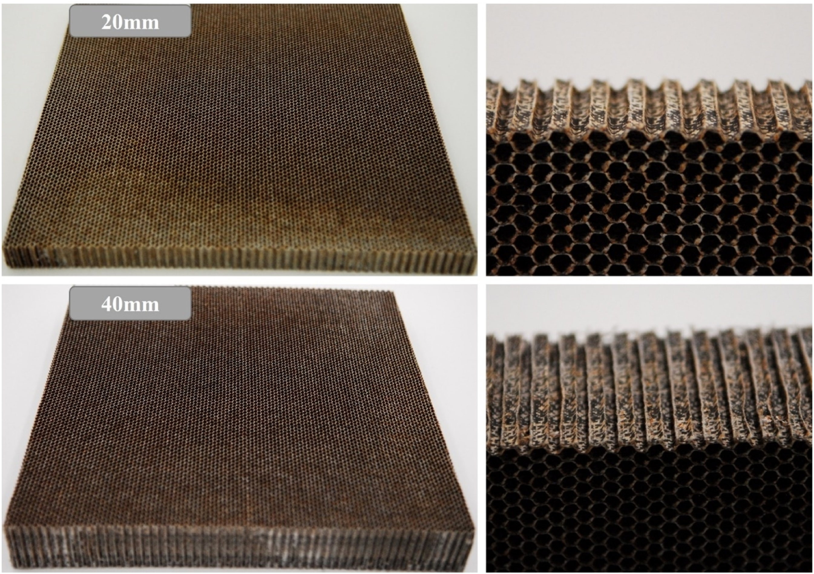
The electromagnetic wave absorption characteristics were measured over a frequency range of 1–18 GHz using the NRL arch method. The S-parameters were obtained using horn antennas and a vector network analyzer. Measurements were performed in two frequency segments, 1–3 and 3–18 GHz, using horn antennas optimized for each band. The specimen was placed at the center of the arch path to minimize interference between the reflected and direct waves. To evaluate polarization characteristics, HH and VV conditions were measured separately by adjusting the specimen. Figure 6 shows a schematic of the NRL arch measurement setup. Schematic of the NRL arch measurement method.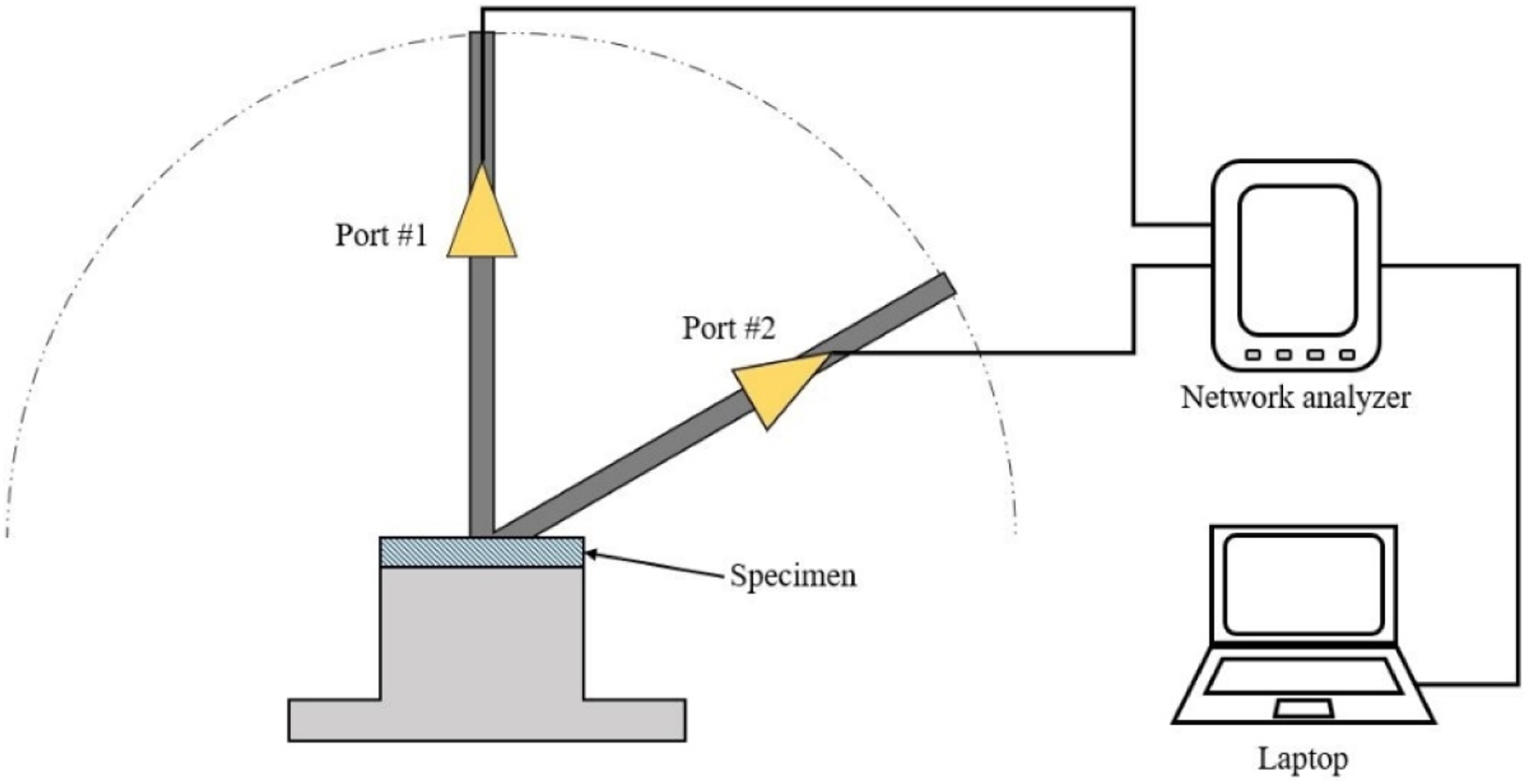
Results and discussion
Figure 7 compares the reflection loss results of the 20-mm and 40-mm specimens obtained using the NRL arch method. For the 20-mm specimen, simulations predicted broadband absorption with a reflection loss below −10 dB across 2.5–20 GHz. Experiments indicated absorption below −5 dB from approximately 1.5 GHz, with a −10 dB reflection loss bandwidth of approximately 14.3 GHz in the 1–18 GHz range. Although the measured resonance frequencies were consistent with the simulated ones, the overall reflection loss was reduced and effective bandwidth was slightly narrower. Measured reflection loss of the pixelated honeycomb absorber with thicknesses of (a) 20 and (b) 40 mm.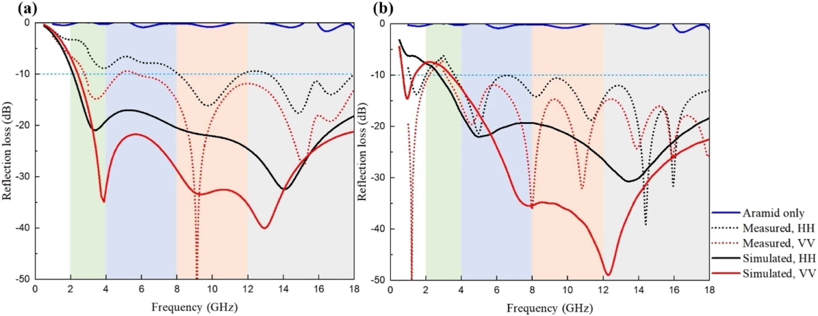
For the 40-mm specimen, fabricated by vertically repeating the same pixelated pattern, simulations predicted absorption below −10 dB over 3.5–20 GHz. Experiments confirmed absorption below −10 dB beginning near 4 GHz, and this absorption was consistently maintained up to the Ku-band. Although the measured performances of both the specimens were lower than those obtained through simulations, the experimental results verified that broadband electromagnetic wave absorption could be achieved with a lightweight, nonmagnetic, and single-layer honeycomb structure. The performance degradation is likely attributable to fabrication-related factors such as pixel misalignment and variations in the conductive ink thickness. To further investigate this degradation, the following section presents simulation-based analyses that estimate the effect of pattern misalignment and provide qualitative evidence for its influence on the absorption characteristics.
This performance degradation is primarily attributed to pattern-printing deviations and alignment errors that occur during fabrication. In particular, the positional misalignment of patterns on the cell walls, non-uniform thickness of the conductive ink coating, and fine gaps introduced during the printing process can lead to uneven surface resistance, which may reduce the absorption performance in specific frequency bands.
Figure 8 presents a simulation-based analysis of fabrication-induced pattern misalignment, verifying this assumption. The coordinates of the top and bottom pixel positions are defined as (xi, yi) and (xj, yj), respectively, with relative offsets along each axis introduced as variables. Simulated reflection loss values for 627 cases of upper (Xi, Yi) and lower (Xj, Yj) pixel misalignments.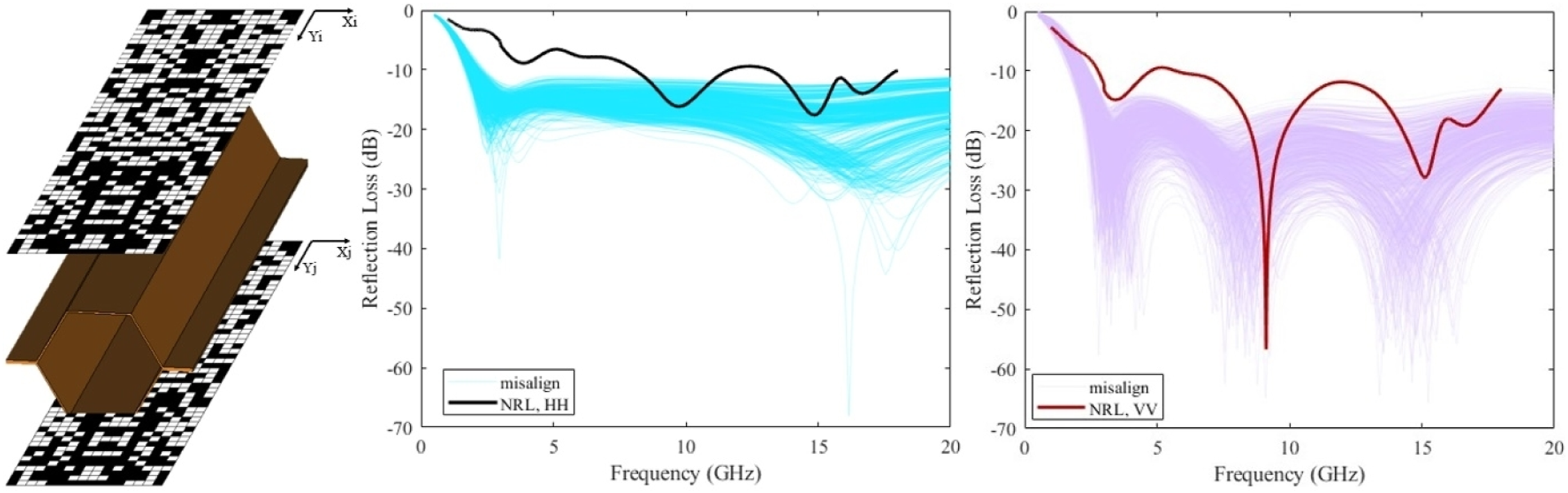
A total of 627 offset cases were generated by independently considering misalignments of the top and bottom pixels, and the corresponding reflection loss curves were plotted. This analysis enabled evaluation of the influence of the pixel offset on the reflection loss and estimation of the error range, thereby providing a reference for explaining the observed performance degradation. Furthermore, the simulation results revealed some variations across the frequency bands, depending on the type of solver used (T-solver vs F-solver) (Figure 9). For the F-solver, the results aligned more closely across the entire frequency range, indicating that frequency-domain simulations more accurately captured the electromagnetic response of the proposed structure. Comparison between the simulated reflection loss results obtained using T-solver and F-solver for the optimized pixelated honeycomb absorber.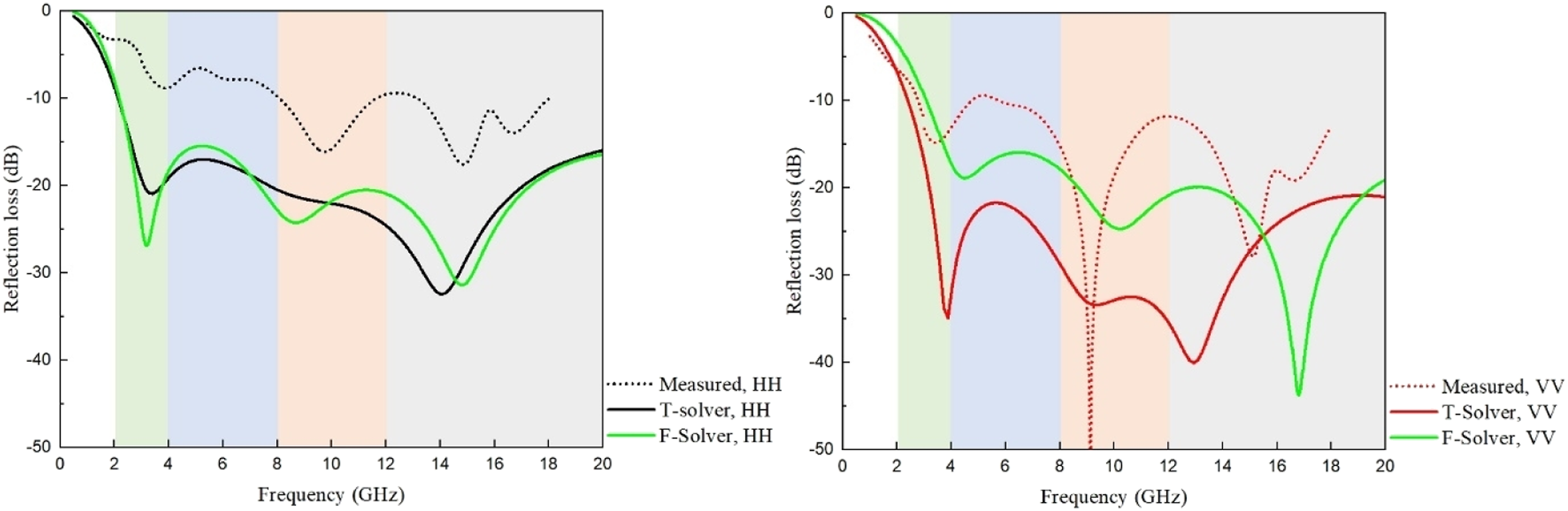
These results suggest that the proposed structure has high potential for practical applications in aerospace and defense systems, in which lightweight characteristics and broadband low observability are critical. In particular, the ability to directly integrate absorption functionality into complex structures—such as aircraft skins, engine inlets, and unmanned-aerial-vehicle platforms—highlights its potential as a structurally functional composite. However, the printing-based process is sensitive to pixel alignment and coating thickness variations, necessitating precise control techniques to ensure stable performance in large-area fabrication. Moreover, as this study primarily focuses on the electromagnetic performance, the mechanical strength and durability of the honeycomb composite remain to be investigated. Extending the developed single-layer design to multilayer structures or more complex geometries, coupled with process optimization, will further enhance its feasibility for integration into operational aerospace platforms.
Conclusion
In this study, we experimentally demonstrated broadband electromagnetic wave absorption using a lightweight, single-layer structure that was 3D pixelated with a conductive ink. A binary pixel grid was introduced onto the internal walls of the aramid honeycomb structure, where each pixel was either filled or left unfilled with the conductive ink and optimized using a GA. The results showed that increasing the thickness from 20 to 40 mm while retaining the same pixel-based design only increased the volume, with limited improvement in the reflection loss performance. This result indicates that simply increasing thickness does not significantly enhance broadband electromagnetic wave absorption. By contrast, the optimized 20-mm-thick structure achieved broadband absorption while maintaining a lightweight configuration, demonstrating that the proposed 3D pixel optimization strategy, rather than simply increasing thickness, is critical for achieving the desired broadband performance. Therefore, the proposed design provides a viable strategy for mitigating the inherent trade-off between thickness and bandwidth. Moreover, the absorber maintained its performance even when the optimized pixel pattern was applied. The density of pure aramid honeycomb was 47.8 kg/m3, while that of the fabricated 20-mm-thick specimen was 50.6 kg/m3, demonstrating that improved functionality can be achieved while maintaining an ultralightweight nature. This result indicates that broadband electromagnetic absorption can be realized with only a minimal increase in the weight relative to the pristine honeycomb structure.
These results validate the practical applicability of the proposed design to complex structural systems, including next-generation stealth aircraft inlets, weapon platforms, and unmanned aerial vehicles. In future studies, more precise control of absorption characteristics and extended performances across wider frequency ranges can be achieved by adjusting the pattern repetition period, refining the pixel resolution, and improving the fabrication stability. Furthermore, the proposed GA-based optimization framework can be extended to incorporate multiple incidence angles and polarization conditions, yielding absorber designs that more closely reflect real operational environments.
Footnotes
Acknowledgments
This study was supported by the Agency for Defense Development [grant number 915047201], funded by the Korean Government.

Ethical considerations
No ethical issues.
Consent to participate
All authors consent to participation.
Consent for publication
All authors consent to publication.
Author contributions
Dohyeong Yoon: Conceptualization, Investigation, Methodology, Software, Validation, Formal analysis, Data curation, Visualization, Writing – original draft. Sangmin Baek: Supervision, Methodology, Validation, Formal analysis, Investigation, Data curation, Writing – review & editing. Wonjun Lee: Conceptualization, Supervision, Project administration, Funding acquisition, Writing – review & editing.
Funding
The authors disclosed receipt of the following financial support for the research, authorship, and/or publication of this article: This study was supported by the Agency for Defense Development [Grant number 915047201], Funded by the Korean Government.
Declaration of conflicting interests
The authors declared no potential conflicts of interest with respect to the research, authorship, and/or publication of this article.
Data Availability Statement
Data will be made available on request.