
Abstract
ZnO and the related ZnMgO and ZnCdO ternary solid solutions are possible alternatives to GaN-based compounds for the fabrication of ultraviolet (UV)/blue light emitting diodes (LEDs) and injection laser diodes. The ZnO materials system has advantages in terms of the higher binding energy of excitons (60 meV), which leads to efficient electron-hole pair-to-photon conversion at the elevated operating temperatures likely for such devices, the availability of commercially available high-quality ZnO substrates, lower growth temperatures (by at least 200°C) and simplicity of selective wet etching processes for mesa formation in devices. Progress in development of ZnO LEDs has been disappointing due to the difficulty of achieving robust p-type doping and the low crystal quality of heterojunctions and quantum wells. We critically review reports of p-type doping using group V impurities as well as progress in growing ternary ZnMgO and ZnCdO films. We also summarise recent progress and prospects for further advancement of ZnO-based light emitters.
Introduction
Zinc oxide, or ‘zinc white,’ a low-priced, powdery white material that is harmless to humans, is widely used for paint pigments, paper coatings, ultraviolet (UV)-absorbing pigments, varistors used for suppressing voltage transients, touch-screen transparent conductive films, gas and biological sensors and filler for rubber goods. ZnO is among a class of materials that have been investigated for realising wide bandgap solid-state p–n junctions for light emission in the blue/UV parts of the electromagnetic spectrum. 1,2 The other materials in this category include CdS, ZnS, ZnSe, GaN and diamond. 3–5 For various reasons, usually involving limitations of doping or the stability of the material during device processing and operation, 6–12 only GaN from this list has been developed commercially to any extent. Light emitting diodes (LEDs) and laser diodes made in the InGaAlN system are available in the wavelength range from about 360–680 nm, with demonstrations of emission as short as 240 nm from high-Al content alloys. 4 InGaN exhibits high emission efficiencies in the violet and blue regions, but longer wavelength devices with high In-content InGaN active regions show a large drop-off in efficiency. 4 To achieve white lighting white light, it is typical to combine a GaN LED emitting in the blue region part of the spectrum with a yellow phosphor. This hybrid approach has yielded luminous efficacies of 249 lm W−1 at a drive current of 20 mA, and 161 lm W−1 at a more typical operating condition of 350 mA drive current. 4
Zinc oxide (ZnO) is an attractive candidate for UV light emission since it is an environmentally friendly material that can be grown at low temperatures on cheap transparent substrates and has both a direct wide bandgap of 3⋅3 eV and a very high exciton binding energy of 60 meV, important for robust light emission. Measurements of near band-edge excitonic photoluminescence (PL) internal quantum efficiency (IQE) yield values for ZnO epitaxial films 9 that are an order of magnitude larger than that for epitaxial GaN. ZnO devices also have the potential for inexpensive LED technology through the use of polycrystalline films deposited on glass. 1,2 In this review we will cover the limitations of current ZnO light emitters, prospects for p-type doping above 1017 cm−3 and carrier injection and a realistic appraisal of ZnO light emitters versus competing GaN-based devices. Other recent reviews have covered aspects of the problems with p-type doping. 13
Properties and attributes of ZnO for UV light emission
Ultraviolet light emitters have many applications, such as solid-state lighting, forensic applications, non-line of sight communications, bio sensors, and air purification systems. It has long been realised that ZnO is potentially well-suited for such emitters, mainly because excess electrons and holes in the material form tightly bound excitons, which lead to very efficient near bandgap recombination at room temperature. Other advantages of ZnO as an emitter, especially with respect to its chief rival, GaN, are the availability of large-area ZnO substrates, the possibility of low temperature epitaxial growth, and excellent radiation hardness. However, GaN (along with AlGaN and InGaN) at present is the only material with existence of a viable p-type doping technology. In one sense, this advanced state of GaN technology is also an advantage for ZnO-based devices, because GaN and ZnO are fairly well matched in lattice constant and thermal expansion, and thus n-ZnO can be grown on either p-GaN or p-AlGaN. Nevertheless, the most desirable solution is to have n-ZnO on p-ZnO, and many groups around the world are working on p-ZnO development as well as growth of homojunction and heterojunction emitters. There is incontrovertible proof that p-ZnO does exist, though with limited conductivity and that its instability can often be traced to noisy Hall-effect measurements or persistent photoconductivity after exposure to light.
ZnO is a direct bandgap semiconductor with E g = 3⋅3 eV. This bandgap can be tuned via divalent substitution on the cation site to produce heterostructures. Alloying with Cd can decrease the bandgap (as low as ∼3⋅0 eV) whereas alloying with Mg can increase the bandgap (as high as ∼4⋅0 eV). ZnO normally forms in the hexagonal (wurtzite) crystal structure with a = 3⋅25 Å and c = 5⋅12 Å. A schematic of the hexagonal lattice structure of ZnO is shown in Fig. 1, along with the bandgap of the related oxides as a function of lattice constant. Note that the ZnMgCdO system covers a fairly similar bandgap range to the more common AlGaInN system. Table 1 summarises the main physical properties of hexagonal ZnO. Note the low hole mobility, high exciton binding energy and high melting temperature, although oxygen is evolved from ZnO crystals beginning around 400°C. Figure 2 shows the temperature dependence of thermal expansion coefficient for ZnO. 14 This is important when considering use of ZnO as a substrate for growth of heteroepitaxial layers.
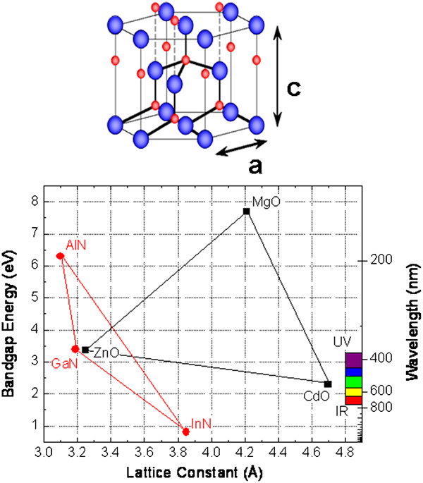
Crystal structure for hexagonal ZnO (top) and bandgap as a function of lattice constant for different compound semiconductor material systems (bottom). In the top figure, the large atoms represent O, the smaller ones, Zn. The ZnCdMgO system covers a similar range of bandgaps as the GaInAlN system
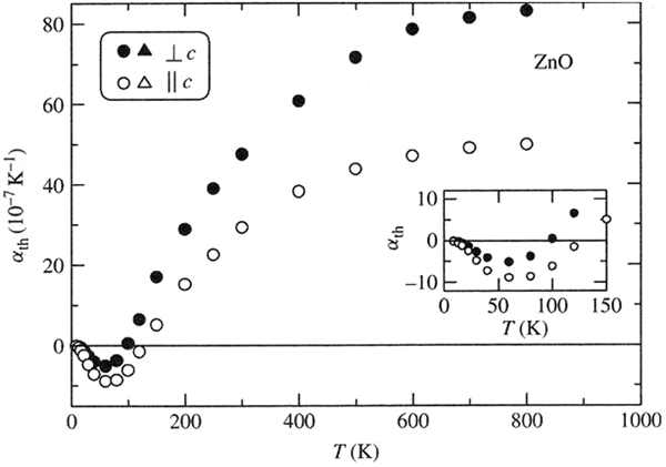
Graph of the ZnO thermal expansion coefficient as a function of temperature. The data is taken from Ibach 14
Properties of wurtzite ZnO
Electron doping in nominally undoped ZnO has been attributed to Zn interstitials, oxygen vacancies, or hydrogen. 1,2,6,7 The intrinsic defect levels that lead to n-type doping lie approximately 0⋅01–0⋅05 eV below the conduction band. 6–8 The optical properties of ZnO, studied using PL, photoconductivity and absorption, reflect the intrinsic direct bandgap, a strongly bound exciton state, and gap states due to point defects. Strong room temperature and near band-edge UV PL peak at ∼3⋅2 eV is attributed to an exciton state, as the exciton binding energy is on the order of 60 meV. In addition, visible emission is also observed due to defect states. These properties make ZnO LEDs potentially useful in efficient solid-state lighting where white light can be achieved by pumping of an appropriate polymer overlayer, as is used in GaN white LEDs. In addition to thin films, it has been suggested that semiconducting ZnO nanowires may offer additional advantages for light emission due to the increased junction area, reduced temperature sensitivity, enhanced polarisation dependence of reflectivity and improved carrier confinement in 1-D nanostructures. 2,13
To realise any type of semiconductor device technology such as ZnO, it is important to have control over the concentration of intentionally introduced impurities, called dopants, which are responsible for the electrical properties of ZnO. 15–34 The dopants determine whether the current (and, ultimately, the information processed by the device) is carried by electrons or holes. In semiconducting oxides, it is generally possible to achieve one or other of these types, but not both with the carrier concentrations needed for light emitting devices. The dopants are also called shallow level impurities because they introduce energy levels close to one of the allowed energy bands in the material and are easily ionised as a result. There may also be unintentional impurities introduced during the growth of ZnO that have a deleterious effect on the properties of the material. These are called deep level defects or impurities and may be either elemental impurities arising from contamination of the growth environment or structural defects in the ZnO crystal lattice. These structural defects can be vacancies in the crystal structure or interstitials, i.e. atoms sitting in the open regions around lattice sites. In both cases, they may introduce energy levels deep within the forbidden bandgap of ZnO and act as traps for carriers in the material. These uncontrolled defects make it very difficult to obtain reproducible device performance and reliability. Using techniques such as pulsed laser deposition (PLD), molecular beam epitaxy (MBE), or even reactive sputtering, ZnO of reasonable quality can be deposited at growth temperatures (at least 200°C lower) lower than that required for GaN. This leads to the possibility of transparent junctions on cheap substrates such as glass or plastic, with the potential to realise low-cost UV lasers or LEDs for high-density data storage (>100 Gb) systems, solid-state lighting (where white light is obtained from phosphors excited by blue or UV LEDs), secure communications, and biodetection. Schematics of PLD and MBE systems for growth of ZnO are shown in Fig. 3. There is a clear need to focus on the use of techniques such as MBE and metal organic chemical vapour deposition (MOCVD) for the growth of ZnO device structures because of the improved crystal quality 14,15 and control of point defects and dopants. It is more common in the literature to see that PLD and sputtering are used for growing ZnO thin films, but the low growth temperatures, absence of high-quality buffers and poorer control of purity and stoichiometry are disadvantages.
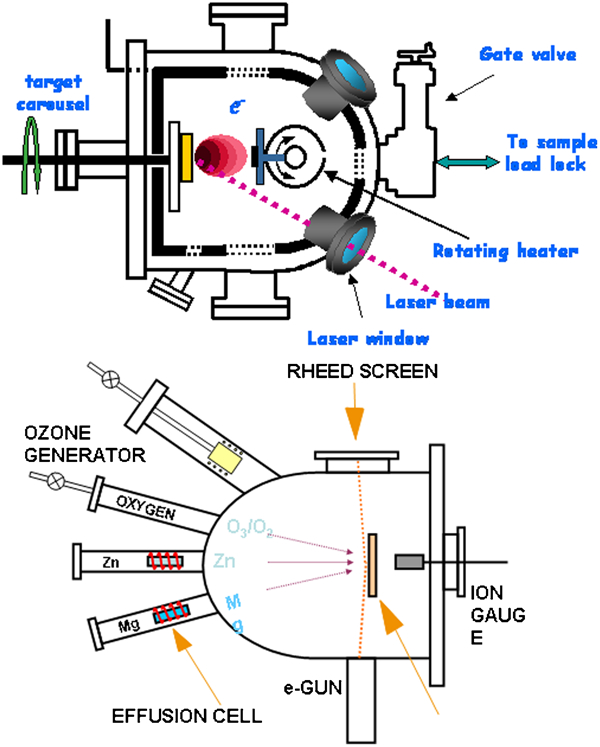
Schematic of pulsed laser deposition (PLD) (top) and molecular beam epitaxy (MBE) (bottom) systems commonly used for growth of ZnO materials
Advantages of semiconductors with a bandgap larger than Si include the ability to operate devices at temperatures and powers well beyond the limits of Si devices, lower noise generation, higher breakdown voltages and ability to sustain large electric fields. Moreover, among the tetrahedrally bonded semiconductors, ZnO has the highest piezoelectric constants with large electromechanical coupling, 2,13 which makes it technologically important for piezo-transducer applications. Although research on ZnO goes back many decades, the renewed interest is stimulated by the availability of high-quality single-crystal substrates and reports of p-type conduction, some of which remain controversial. 1,2,13
One of the critical issues in the exploitation of standard ZnO materials in optoelectronic applications is the effective injection of minority carriers (holes) resulting in radiative recombination. It has proven difficult to achieve reproducible p-type doping of ZnO, a situation similar to that of GaN in the early 1990s. 4 Doped ZnO has been used as anode material for organic LEDs because of its chemical stability, high transparency and relatively high work function. Hybrid LEDs with n-type ZnO as an electron injector has been realised in many different systems, but true p–n homojunction injection devices have shown very low band-edge emission efficiency.
Owing to the difficulty in growing p-type ZnO, metal–insulator–semiconductor (MIS) diodes and p–n heterojunction LEDs were the first demonstration structures. For the fabrication of p–n heterojunction LEDs, n-type ZnO films were grown on other p-type materials such as SrCu2O2, CuGaS2, GaN and AlGaN owing to the lack of reliable p-type ZnO layers.
Limitations of ZnO for UV light emission
The main limitations of all wide-gap semiconductors (defined here as having bandgaps above 2⋅5 eV) for these types of applications are related to doping: usually either donors or acceptors tend to have large ionisation energies because they lie deep in the bandgap, and thus have small fractional ionisations at room temperature. The lattice energetics of wide bandgap semiconductors tend to favour either efficient donor or acceptor doping, but not both, as described above. 2 In the case of ZnO, donors always tend to be dominant, and moreover are easily formed as compensation centres if acceptors are deliberately added. There are potential ways to mitigate these problems to some extent, as has been found for GaN, and thus much effort has been directed at finding solutions for ZnO. Success has varied, and some claims of p-type ZnO are obviously flawed and lack the necessary evidence for claiming p-type conductivity. There are a number of checks that should accompany any claim of p-type conductivity and as will be seen later, observing band-edge emission from a structure ostensibly containing a p–n junction is a necessary but not sufficient condition because holes may be created by impact ionisation in the depletion region near grain boundaries in polycrystalline ZnO. 20,21 Mahan et al., 21 explained the conduction in ZnO-based metal-oxide varistors by invoking hole creation by impact ionisation during biasing. Direct evidence of the production of holes in forward-biased ZnO varistors was later reported by Pike et al. 20 with the detection of band-edge electroluminescence (EL) in addition to the broad subband-gap luminescence peaked near 600 nm. Thus, what might appear to be evidence for presence of a p–n junction might simply be a recombination of electrons and holes in an MIS structure. 19–21 The likelihood of this occurring is made more plausible by the typically low band-edge to deep level emission ratio in many reports of ZnO LEDs.
Another issue is the correct interpretation of conductivity type measurements and use of corroborating evidence to support the assignment of p-type conductivity. For low carrier density, low mobility semiconductors, Hall measurements can be challenging given difficulties with contacts, inhomogeneity in sample geometry, and relatively small Hall voltage signals. At a minimum, both the Hall coefficient and Seebeck coefficient must be used to determine the carrier type and the conductivity type inferred from the Hall voltage versus magnetic filed behaviour. Temperature-dependent Hall measurements allow extraction of activation energies for dominant dopant levels and to differentiate transport effects that originate from two separate conduction channels. 8 In ZnO, a second relevant channel for conduction is often a conductive surface layer that nearly always dominates at low temperatures in lightly doped material, because of freezeout of the bulk carriers. 8 However, for p-type samples, which have lower bulk conductance, the surface conduction will be more important, and must be understood and taken into account. An important piece of evidence for the conductivity type is MIS structures, whose capacitance–voltage (C–V) characteristics can be used to extract carrier properties from gated structures. Figure 4 shows C–V plots for undoped ZnO and p-doped ZnMgO MIS structures. The polarity of the voltage needed to deplete the structure provides a direct means of determining the majority carrier type in a semiconductor material. 12 In particular, the symmetry of the C–V behaviour in MIS structures is dependent on the majority carrier type underneath the gate. Depending on the majority carrier type, the MIS capacitance is maximised when bias accumulates majority carriers at the semiconductor/insulator interface. For n-type material, a positive voltage relative to the semiconductor will maximise capacitance. For p-type, a negative voltage is needed to accumulate majority carrier holes. The MIS structures in Fig. 4 were fabricated with both n-type ZnO and phosphorus-doped (Zn,Mg)O thin films. The polarity of the C–V characteristic for the device employing nominally undoped ZnO is clearly n-type, with capacitance decreasing with an applied negative voltage. For the (Zn,Mg)O:P device, the symmetry is p-type. With a phosphorus content of 2 at.-%, one can estimate the activation energy of the acceptor in the p-type material to be in the order of 180–200 meV, consistent with the expected ionisation energies of group V-related acceptor complexes in ZnO. 21–34
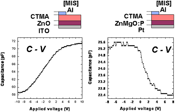
Capacitance–voltage (C–V) characteristics of metal–insulator–semiconductor (MIS) structures containing n-type ZnO (left) and p-type ZnMgO doped with P (right)
Native defects
Compensation by native point defects and their complexes plays an important role in influencing the efficiency of doping in ZnO and related alloys. 35–77 These compensating centres may be native defects like vacancies or interstitials from either sublattice or complexes thereof or simply impurities. 39,48,51,52 At high enough levels, the doping itself can induce self-compensation. This is a common phenomenon in other compound semiconductors such as GaAs, where the formation energy of acceptor-like Ga vacancies in n-type material decreases as the Fermi level rises closer to the conduction band-edge. The understanding of native defects in ZnO is still far from complete 51,52 and has been largely driven by first principal calculations using different approaches. The formation energy of these defects is generally dependent on the position of the Fermi level.
It is generally accepted that VO is a deep donor having so-called negative U behaviour, or the ability to trap two electrons (or holes) with the second bound more strongly than the first. This indicates the presence of a net attraction between the two carriers at the defect or a negative Hubbard correlation energy U. The result is that the defect energy levels in the gap are inverted from their normal order. Different reports in the literature place the energy level for the oxygen vacancy from 0⋅8 to 3⋅72 eV depending on the approximations used in the calculations. 51,52,58,60–63 The formation energy of VO increases as the Fermi level moves towards the conduction band-edge. VZn is calculated to a deep acceptor with two ionisation states at 0⋅18–0⋅9 eV for the 0/−1 state and 0⋅87–2⋅4 eV for the 1/−2 state. This is one of the most common acceptors in n-type ZnO. The Zn interstitial is usually calculated to be a shallow donor, with a high formation energy in n-type ZnO of ∼4 eV for Zn-rich conditions), but much smaller as the Fermi level moves closer to the valence band-edge. ZnO is a donor with high formation energy (>3 eV) in n-type ZnO and low formation energy (<1 eV) in p-type ZnO. Oxygen interstitials and OZn also have high formation energies.
The difficulty in achieving p-type doping for ZnO is related to the formation of compensating defects, the low solubility (typically <1018 cm−3) of the acceptor dopants, and the large ionisation energy (170–380 meV) of all the acceptor candidates. 56,64–67 Most of the previous studies on p-type ZnO have focussed on addressing the low solubility and high ionisation energy of the acceptors. NO is the acceptor with the lowest ionisation energy: the actual value depends on the calculational method but it is usually determined to be ∼170 meV). Co-doping with N and a group III element has been studied in an attempt to increase the solubility of N through the formation of the IIIZn–2NO complex. The substitutional dopants AsO, PO and SbO are deep acceptors in ZnO. However, PZn(VZn)2 and the As and Sb analogues are shallower acceptors exhibiting lower formation energies. 76 A schematic of the PZn(VZn)2 complex is shown in Fig. 5. 48 Both the VO and Zni defects have low formation energy for p-type ZnO and thus could be compensating centres. Hydrogen impurities may also play a role as a compensating donor for p-type ZnO. 11 There is still a strong need to understand the origin of the compensating defects in ZnO and related alloys, and to understand their dependence on the Fermi level position. 2,11,13
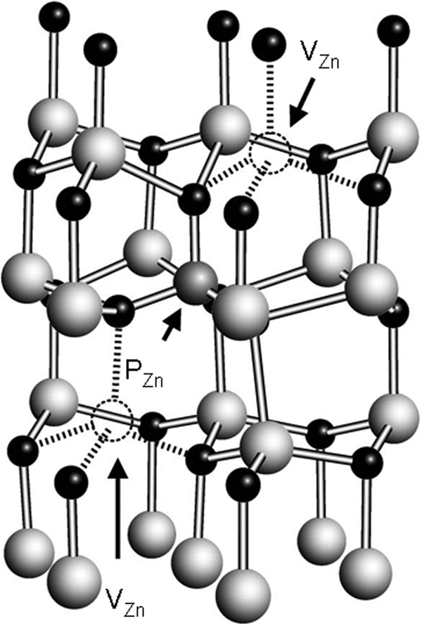
Model of P–2V acceptor complex thought to be responsible for p-type conduction in P-doped ZnO (adapted from Limpijumnong et al. 48 )
As an example of such a study, first principle calculations show that the formation of Ga acceptor complexes GaZn–VZn and GaZn–Oi are energetically favourable at high Ga concentrations. 67,77 Experimentally, the formation of VZn with concentrations near 1020 cm−3 were found when doping with ∼1021 cm−3 Ga in PLD grown ZnO. Similarly, the presence of VZn related defects at a concentration of ∼1019 cm−3 was found when doping with 1020 cm−3 Ga atoms. This work also suggested that electrical inactive VZnH2 complexes were formed during post-growth annealing in hydrogen. The formation of the high concentration of VZn defects could be due to the decrease of the VZn formation energy with the Fermi level moving towards the conduction band-edge.
p-type ZnO
It took many years to produce efficient GaN-based LEDs because of a lack of p-type doping capability. 4 A similar situation holds for ZnO. 41,78–97 Crystal defects occur easily in zinc oxide, and they tend leave ZnO with a residual n-type conductivity. 8 In order to turn this n-type semiconductor into p-type material, one must remove these defects from the zinc oxide film, and thereby lower the n-type background doping as much as possible. Once a nearly ‘non-n-type’ state is reached, the second step consists of introducing nitrogen or other acceptors into the crystal to transform the film into a p-type semiconductor. Since nitrogen evaporates easily in ZnO, it was difficult to mix it with the crystal, but this eventually was resolved through a method known as ‘repeated temperature modulation,’ where the film crystal growth temperature is repeatedly switched between 400 and 1000°C, leading to lightly p-type zinc oxide. 25,87,88 Zinc oxide p–n junctions were then created and, by passing a current through them, clear blue-colour light emissions (around 400 nm) were produced.
The recent progress in ZnO science and technology has included numerous reports of p-type doping with a few different acceptors, 2,13 better control of background n-type conductivity in most films, the identification of some of the residual donors, and improved contacts. Significant progress has been made in achieving high-quality (defined as x-ray diffraction peak widths of a few hundred arc seconds or less), single-crystal substrates. n-type conductivity is relatively easy to realise via excess Zn or with Al, Ga, or In doping, but p-type doping is problematic, because there can be compensation by native point defects or dopant atoms that locate on interstitial sites. The main candidates for this compensation are usually thought to be the native donors VO, ZnI and also the Zn anti-site defect, all of which have low formation energies in p-type ZnO and could result in hole compensation.
The defect compensates for the substitutional impurity level through the formation of a deep level trap. In some cases, strong lattice relaxations can drive the dopant energy level deeper within the gap. In other systems, one may simply have a low solubility for the chosen dopant, which limits the accessible extrinsic carrier density. In ZnO, most candidate p-type dopants introduce deep acceptor levels. 2,13 There can also be compensation of acceptors by donor impurities such as hydrogen, 11 a common component of growth ambients. Finally, there are issues with the low solubility of many acceptor dopants and large ionisation energies of these species in ZnO. Theory suggests that the O vacancy is a deep donor and while the Zn interstitial and anti-site are both shallow donors, these defects are expected to be present only at low concentrations in thermal equilibrium. 51,52 This reinforces the notion that there are other sources of n-type conductivity, such as hydrogen, the shallow donor state of the O vacancy, and defect complexes involving the Zn interstitial. 11 Concerning native defects that are acceptors and could compensate n-type material, the deep acceptor Zn vacancy seems like the prime candidate. The O interstitial and anti-site are high in formation energy and/or are electrically inactive and, hence, are unlikely to play essential roles in electrical properties.
A number of different growth techniques, acceptor species, and substrates have been used for the successful growth of p-type ZnO. 1,2,13 Some data on ZnO diodes have been reported in the literature. 1,2,6 There have been at least seven different growth techniques, eight different materials for the p-type layer, and seven different acceptor dopants used in the fabrication of the various diodes. 13 Some of them have been designed as photodiodes, and some as photo-emitters. Within the latter group, several different emission wavelengths have been reported from the violet into the blue region of the spectra. Table 2 shows a list of the potential acceptor dopant candidates for ZnO.
Valence and ionic radii of candidate dopant atoms
Many of the attempts to produce p-type ZnO have employed N as the acceptor of choice. 26–34 In fact, N is a natural choice for an acceptor dopant, since it has about the same ionic radius as that of O, and thus should readily substitute for the latter. It has been suggested that co-doping, such as an N–Ga–N complex will be more soluble than N alone, and moreover it will be a shallower acceptor. 13 There has been some experimental work done on this premise, but a potential problem is that isolated Ga atoms will tend to compensate the N–Ga–N acceptors. 2,13 Nitrogen should be a good choice as a p-type dopant in ZnO since it acts as a shallow acceptor in other II–VI compounds and is the most suitable anion-site acceptor in ZnO from both atomic-size and electronic-structure considerations. While there are reports of successful p-type doping of ZnO with nitrogen, the conductivity is often degraded with time after growth. In addition, despite the fact that N might be incorporated as a shallow acceptor with an ionisation energy of 170 meV, the doped ZnO may remain either semi-insulating or n-type due to the sensitivity of the state of the nitrogen on several factors. For example, the N incorporation may be affected by the polarity of ZnO and even when N is incorporated in ZnO its efficiency as an acceptor is expected to largely depend on the local surroundings and the presence of other impurities. For example, nitrogen substituting for oxygen, NO, is calculated to be a deep acceptor with an energy level of E v+(1⋅6–1⋅7) eV. On the other hand, the acceptor ionisation energy is predicted to be significantly reduced if (i) NO is surrounded by isovalent group II atoms substituting Zn; (ii) NO is a part of complexes with residual group III contaminants (Al, Ga, In); or (iii) NO forms the NO–H–NO complex. In addition, the electrical activity of N can be largely affected by the presence of various intrinsic defects that can act as efficient compensating centres and also facilitate formation of various N-related complexes, including donor complexes of ON or ZnI–NO.
Group I elements, substituting on the Zn site, are also acceptor candidates. Li, Na, and K, are predicted to have acceptor energy levels of 0⋅09, 0⋅17, and 0⋅32 eV, respectively. 51,52 These levels are shallower than those predicted for NO, PO, and AsO. First-principles calculations showed that group I dopants such as Li and Na show strong self-compensation of the substitutional acceptors by interstitial donors. 39,63 It was suggested that co-doping with hydrogen to form complexes with the substitutional acceptors would suppress formation of these compensating interstitials. 11 Post-growth low temperature annealing could then dissociate the passivated acceptors and reveal their electrical activity. 11
Among the most promising dopants for p-type material are the group V elements, based on the possibility to obtain holes via substituting −3 anions for the −2 oxygen sites. There have been reports of acceptor behaviour with phosphorus, arsenic, and antimony. 23,46 The conversion of transport behaviour from highly conducting to semi-insulating with annealing may be attributed to at least two factors. 12 First, the defect associated with the shallow donor state in the as-deposited films appears to be relatively unstable. The dependence of post-annealed resistivity on the p-content suggests that a deep level associated with the p-dopant is present. 12 This is consistent with the expected results that p-substitution on the O site yields a deep acceptor. Figure 6 shows the conversion of p-doped ZnO(top) and ZnMgO(bottom) to p-type conductivity as a function of either post-growth annealing (top) or the O2 partial pressure during growth. The P-dopant is quite thermally stable in ZnO, as shown in the secondary ion mass spectrometry (SIMS) data of Fig. 7, which shows alternating layers of undoped ZnO and p-doped ZnMgO before and after annealing at 750°C. The potential for doping ZnO with phosphorus was examined via first-principles pseudopotential calculations. 23,24,36 There is a large size mismatch between P and O (the ionic radius of phosphorus (2⋅12 Å) is much larger than oxygen (1⋅38 Å) and the size mismatch should favour substitution on the Zn site to alleviate lattice strain) and the calculated acceptor level for substitutional P (PO) at an O lattice site was found to be deep in the gap (0⋅67 eV above the VBM). Substitutional P (PZn) at a Zn anti-site was found to be a triple donor with ionisation levels lying near/above conduction band-edge. In O-rich growth conditions, Zn vacancies (VZn) were double acceptors and were predicted to be energetically more favourable than the PO acceptors. The PZn–2VZn defect complex was found to be a single shallow acceptor with an ionisation level 0⋅18 eV above the VBM. The energy lowering interactions between the PZn defect and two Zn vacancies stabilises the formation of a PZn–2VZn complex, resulting in a shallow acceptor level. 44,45
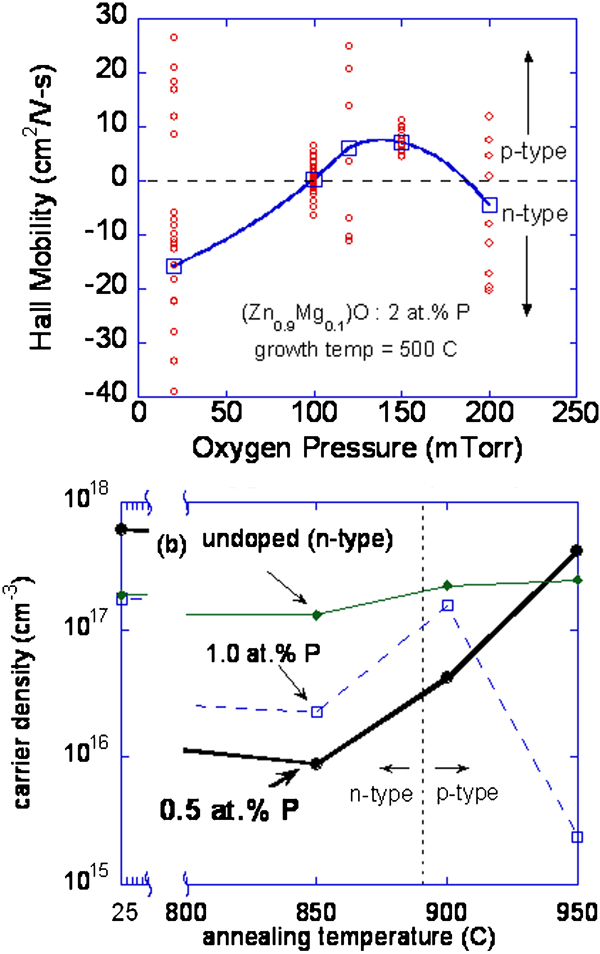
Carrier density as a function of annealing temperature for undoped, 0⋅5 and 1⋅0 at.-% p-doped ZnO films (top) and Hall mobility in p-doped ZnMgO as a function of O2 partial pressure during pulsed laser deposition (PLD) (bottom)
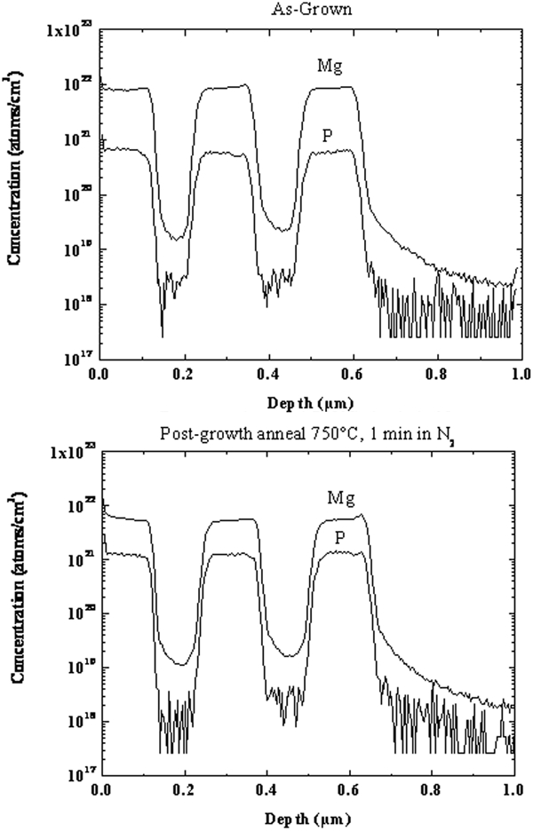
Secondary ion mass spectrometry (SIMS) profiles of ZnO/ZnMgO:P multi-layer structures before (top) and after 750°C annealing (bottom)
There is also a note of caution with respect to the interpretation of these shallow acceptor defects. Janotti and Van de Walle 51 have suggested that the formation energetics of the AsZn–2VZn, SbZn–2VZn and PZn–2VZn complexes are not favourable and other ab initio calculations indicate that these may have deeper acceptor states than needed to explain the p-type conductivity and that interstitial vacancy complexes of these impurities are more likely, with suggested configuration (As,P,Sb)I–3VZn. 64
It seems clear that many of the reports of high p-type doping levels in Sb-doped ZnO in particular are in error because of the high mobilities in the doped layers and also the low efficiency of LEDs fabricated on the material, suggesting it is actually n-type. 35,37,38 Liu et al. found in ZnO grown by plasma assisted MBE, that over a wide rage of Sb concentrations, the Sb predominantly occupied Zn sites and exhibited donor activity, 35 consistent with past implant and doping studies. 36 However, as noted earlier, the sensitivity of electrical properties to growth conditions does not preclude formation of the divacancy defects discussed above under different growth methods.
Specific strategies for overcoming p-type doping bottlenecks in wide bandgap semiconductors were outlined by Zunger and co authors 97 and include (i) alloying with an element that leads to an upward bowing of the valence band maximum, (ii) designing growth conditions that destabilise anion vacancies and/or cation interstitials, (iii) enhancing anion/cation dopant solubility by growing under poor host anion/cation conditions, and (iv) decorating the dopant by strongly bonding ligands that enhance local chemical bonding energy but do not disrupt the host bonds. To date, the observed mobilities for p-type phosphorus-doped ZnO have been relatively low. There are also open questions regarding the stability of the acceptor states, the role of surface conductance in yielding apparent instabilities in transport measurements, and the origin of high leakage current channels for p–n structures. Important issues that need to be addressed include maximising hole concentrations in the p-type region, improving crystalline perfection of the junction interface, minimising point defects associated with anion stoichiometry and extended defects that originate from the substrate/film interface. Note that similar limitations were encountered and overcome in other semiconductor systems, including AlGaAs and GaN. Each required concerted efforts to improve our fundamental understanding of materials processing and properties, both in terms of reduction in unwanted defects and introduction of active substitutional defects for effective doping.
If a sample of p-type ZnO i s exposed to strong UV light, and then returned to a dark condition, it will remain p-type at lower temperatures but then become n-type at higher values of temperature and remain n-type up till room temperature is reached. 26 This is a reversible effect, meaning that the sample will return to p-type if the temperature is lowered. If held at room temperature, the sample will remain n-type for many hours, but will gradually anneal back to p-type. The existence of a transition from p-type to n-type, and back to p-type, leaves no doubt that p-type ZnO does exist, and also provides a reasonable explanation of why p-type ZnO sometimes seems unstable. Figure 8 shows a summary of reported electron or hole concentrations in doped ZnO. Note the much higher values for donor dopants.
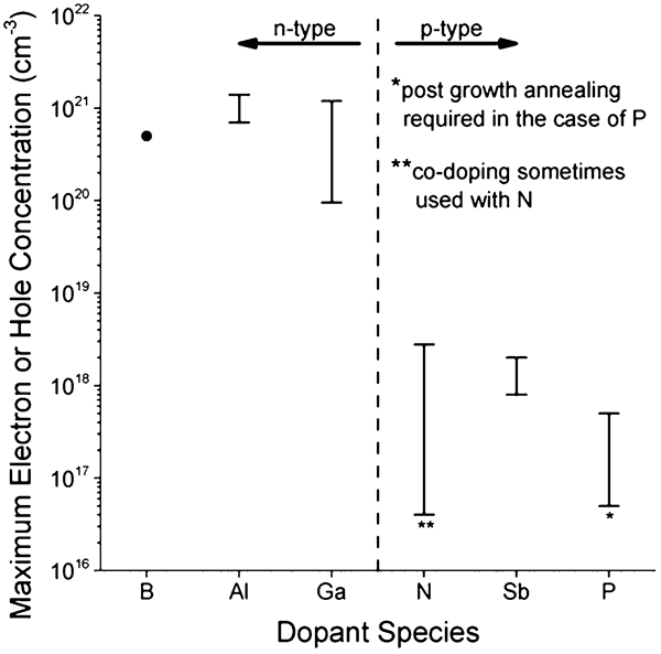
Maximum reported electron or hole concentrations in ZnO for different dopants
Future approaches to p-type doping
Among the II–VI semiconductors, the only compound that readily exhibits p-type conductivity with all group V dopants is ZnTe. In ZnTe, a p-type carrier density of 1020 cm−3 is achievable. This largely reflects the fact that the valence band maximum in ZnTe is significantly higher than that seen in other II–VI semiconductor compounds. Extensive studies of II–VI materials indicate that the local bonding environment for the anion determines both the solubility and ionisation energy of the dopants. In theory, we would anticipate a shift in ionisation energy if a group V dopant is codoped with an isoelectronic group VI element. As such, it is useful to consider the effect of isoelectronic Te substitution into ZnO on the doping behaviour of group V dopants on the O site, or group I substitution on the Zn site. In II–VI semiconductors, the behaviour of isoelectronic impurities largely depends on the difference in electronegativity of the dopant relative to the anion or cation it is replacing. For large differences, isoelectronic substitution can yield a bound exciton or acceptor state with no additional dopants. It has been observed that oxygen doping of some II–VI semiconductors yields an acceptor state whose origin is unclear but may be associated with a defect structure involving interstitial O. While oxygen doping of various II–VI semiconductor has been explored, little work has addressed the possible effects of isoelectronic anion substitution on the conductivity type in ZnO. It can be postulated that the substitution of a less electronegative anion may locally raise the valence band maximum, potentially facilitating the formation of acceptor states effective in producing difficult carrier type conductivity. Limited work reported on Te-doped ZnO showed a significant reduction in carrier density due to defect donor states, with the carrier type being indeterminate. Additional evidence that isoelectronic doping in ZnO yields shifts in dopant activation behaviour can be seen from Mg doping in ZnO. In this case, a decrease in electron density is observed with Mg doping presumably due to a shift in the conduction band relative to the vacuum level and defect donor states. The fact that ZnTe does not assume the wurtzite structures suggests a limited solubility of Te substitution on the O site. Therefore, it may pay to investigate both Te and Se as isoelectronic codopants. MgTe is a wide bandgap wurtzite semiconductor with a bandgap of 3⋅47 eV, and an extrapolated valence band maximum predicted to be close to that for ZnTe. Thus, the solubility of Te in ZnO may be enhanced by co-doping with Mg and synthesis of (Zn,Mg)(Te,O) thin films may be fruitful. Previous work on Te-doped ZnO indicates enhanced solubility of nitrogen for films deposited by PLD with a nitrogen plasma.
Owing to the problem of p-type doping of ZnO, it has been a major challenge to achieve efficient operation of bipolar devices. Light emitting diodes with ZnO active region have, however, been successfully demonstrated utilising p-AlGaN, p-SiC, p-diamond, as well as p-AlGaN/p-GaN heterostructures for hole emitters. 41,78–81,86,90 Owing to chemical and crystallographic differences between ZnO and AlGaN (SiC or diamond), the formation of defects at the hetero-interface can negatively impact optical and electrical properties. Therefore, devices formed from the heterostructures are expected to be inferior to all ZnO-based devices.
The problems with p-type doping of ZnO discussed earlier is similar to that encountered in the early development stages of GaN. In ZnO, donors act as compensation centres if acceptors are deliberately added as needed for p-type injection layers. Background n-type concentration can be lowered by incorporating Mg in the lattice of ZnO, to increase the bandgap, and then doping the ZnMgO with group V acceptors at high concentrations, followed by annealing, to obtain conversion to p-type conductivity. 89 Device quality nitrogen-doped p-type thin epitaxial ZnO films are more likely to be achieved by MOCVD and MBE. The lack of p-type behaviour in nitrogen-doped ZnO has been addressed theoretically within the context of N–N complex formation. Isolated substitutional N is assumed to be required in order to realise the desired acceptor state. As an example of the expected higher quality growth with MBE, homoepitaxial nitrogen-doped ZnO was grown on semi-insulating Li-doped ZnO crystals from a high purity Zn evaporation source, combined with atomic O and N flux created via an RF plasma. Hall measurements yielded p-type behaviour with a hole mobility of 2 cm2 V−1 s−1 and a hole concentration of 9×1016 cm−3. The acceptor level was estimated using low temperature PL to be 170–200 meV. This result was dependent on minimising the concentration of compensating donor levels from defects or complex formation.
What are some potential future areas of research where p-type doping of ZnO might be improved? There are a number of possibilities:
improve the crystal quality and purity of the ZnO films. It is generally accepted in other compound semiconductors that thick buffer layers, high purity precursors and high growth temperatures are required to produce device-quality films. This may require a more concerted move from techniques like PLD to MBE and particularly MOCVD, which are more amenable to purity control, buffer optimisation and stoichiometry control. For example, in situ techniques like Reflection High Energy Electron Diffraction can be used to examine surface crystallinity during MBE and then to optimise the growth mechanisms. Another possibility is to employ atomic oxygen to lower the density of oxygen vacancies. In order to maximise hole density in acceptor doped materials, one would like to drive the background carrier density even lower while maintaining PL efficiency. There is continuing debate regarding the origin of the native shallow donor state in ZnO. Yet, it is clear that oxygen vacancies and/or Zn interstitials yield defect states that negatively impact the ability to control transport properties in these materials. It would be useful to investigate the use of atomic oxygen as the oxidising species. There is also a need for more attention to issues like substrate surface cleaning and preparation and nucleation of the ZnO layer. At this stage of ZnO doping studies, it is fair to point out that these processes are at a much earlier point in development than materials such as GaN. Another example is the development of better buffer layers, such as an investigation of thick semi-insulating buffer layers such as Zn0⋅8Mg0⋅2O or ZnO:Cu to reduce defect density in the active layer. In developing LED structures for GaN, it is well known that the use of thick (∼1 μm) buffer layers is instrumental in the reduction of extended defects that originate from the from the film/substrate interface. Ideally, one would prefer this buffer layer to be insulating so as to confine electrical conduction to the active device region. In PLD growth, both (Zn,Mg)O and ZnO:Cu yield semi-insulating thin films and this should be transferable to MOCVD and MBE.
Translate the work on group V doping to these more advanced epi growth techniques. For as-deposited p-doped films grown by PLD, the inclusion of phosphorus yields a significant increase in electron density, resulting in ZnO that is highly conductive and n-type. In the case of undoped material, the reduction in donor density is presumed due to either a reduction in oxygen vacancies, Zn interstitials, or perhaps out-diffusion of hydrogen that is incorporated in the ZnO lattice during synthesis. All of these should be reduced by going to MBE or MOCVD growth.
Look in more detail at post-growth annealing. In PLD films, the resistivity of as-deposited phosphorus-doped films was significantly lower than that for the nominally undoped film, with a shallow donor state dominating transport. After annealing, the resistivity of the phosphorus-doped films increased rapidly, as shown in Fig. 6. When annealed at 700°C, the phosphorus-doped ZnO films became semi-insulating with a resistivity approaching 104 Ω cm. The conversion of transport behaviour from highly conducting to semi-insulting with annealing should be attributed to at least two factors. First, the defect associated with the shallow donor state in as-deposited films appears to be relatively unstable. The dependence of post-annealed resistivity on phosphorus content suggests that a deep level associated with phosphorus dopant is present. This is consistent with the expected results that P-substitution on the oxygen site yields a deep acceptor. Post-growth annealing can be expected to substantially alter the electronic properties, depending on the ambient conditions. The removal of hydrogen from Mg-doped GaN was the key step in achieving p-type conductivity in that material. A detailed investigation of transient heating during growth to achieve activation of acceptor dopants (phosphorus, nitrogen) during growth would be valuable. For the substitution of group V dopants on the oxygen site in ZnO, the solid solubility is limited. This can potentially be overcome by in situ doping in films deposited at relatively low temperatures. However, low temperature growth also results in a higher density of defects, due to limited kinetics for crystallisation, that yield shallow donor states. In order to achieve optimal properties, we will investigate the use of transient heating during growth, in which the substrate temperature is periodically ramped up at intervals of several monolayer growth. This approach has been reported for nitrogen-doped materials, but has not yet been applied to phosphorus. For the substitution of group V dopants on the oxygen site in ZnO, both solid solubility and dopant activation are apparent limiting factors. This can potentially be overcome by in situ doping in films deposited at relatively low temperatures. However, low temperature growth also results in a higher density of defects, due to limited kinetics for crystallisation, that yield shallow donor states. It also limits the activation of the dopants as acceptor states. It has been reported that subjecting the films to a spike anneal is effective in activating acceptor states for nitrogen-doped ZnO materials. 25 The transient heating effectively serves as a rapid thermal anneal of deposited layers in which the dopant is incorporated at low temperature, but annealed briefly at high temperature to improve crystallinity and activation of the dopant. Transient heating during growth of ZnO doped with P and As, in which the substrate temperature is periodically ramped up at intervals of several monolayer growth, might enhance the dopant activation. This transient heating should be examined for varying temperature cycles and oxidation conditions.
Use of alloys such as ZnMgO in which background donor concentrations are low. p-type conductivity has been reproducibly achieved for (Zn0⋅9Mg0⋅1)O:2 at.-% P epitaxial films grown by PLD (typical Hall mobility ∼5–10 cm2 V−1 s−1 and carrier density ∼3×10¹⁶/cm3) The p-type behaviour was systematic with oxygen pressure during film growth with no post-annealing performed. Figure 6 shows a plot of these four voltage pairs for the 0⋅5 at.-% p-doped ZnO film grown at 700°C in 150 mTorr oxygen, followed by rapid thermal annealing at 900°C. Secondary ion mass spectrometry profiles show no evidence for P diffusion or segregation for annealing temperatures up to 1000°C.
Investigate delta doping with ultrathin ZnTe:P. One approach that has proven effective in yielding enhanced hole concentrations in ZnS and ZnSe is to insert single monolayers of heavily p-type doped ZnTe periodically throughout the thin-film structure. This so-called δ-doping was used to achieve hole densities on the order of 7×1018 cm−3 for ZnSe δ-doped with ZnTe. Such an approach should prove useful in achieving high hole carrier densities in ZnO. We will also investigate through modelling initially the use of p-type ZnO/ZnCdO graded superlattices (SLs). This approach has been successful in nitride-based structures. Carrier transport simulations show that significantly improved vertical and lateral electrical conductivity (σV and σL) can be achieved in p-type GaN/InGaN SLs utilising composition-graded p-InGaN layers. Compared to typical modulation-doped SLs, the barrier height and the sheet-hole density in the p-InGaN wells were, respectively, more than 8 times lower and 2⋅6 times higher. This achievement is due to the combination of a number of factors, including polarisation charge distribution in the graded layers, an adjusted Mg-doping profile, and a shallower acceptor activation energy in InGaN. The optimised SL design leads to an improvement of more than eleven orders of magnitude in σV compared to typical SLs while maintaining a value for σL that is better than that of bulk p-InGaN. Both σV and σL are found to improve at higher temperatures in the optimised structure. A similar approach may be useful for ZnO LEDs.
Optical properties of ZnO
The optical properties of ZnO are usually studied by PL, although cathodoluminescence (CL), optical absorption/transmission/reflection, photoreflection and spectroscopic ellipsometry are also common. 98 Typical PL spectra for ZnO consist of a sharp peak near the band-edge peak and a broad (midgap) band around 2⋅4–2⋅5 eV in the green/orange region. The sharp lines dominating the band-edge region of the spectra originate from excitons bound to neutral acceptor or donor atoms. At slightly lower energies are longitudinal optical (LO) phonon replicas while free exciton transitions with the valence band occur at slightly higher energies. There may also be two-electron satellite recombination lines of the neutral donor bound excitons and donor–acceptor pair transitions at ∼3⋅22 eV. Figure 9 shows the temperature dependence of the PL spectrum of undoped ZnO in the near band-edge region. Note that the free electron-acceptor transition, (e,A0), appears above 30 K as the donor–acceptor pair (DAP) transition at 3⋅220 eV disappears. 54 The dominant donor in this material was determined to be hydrogen, with an ionisation energy of around 30 meV, while the acceptor was suggested to be substitutional N atoms on oxygen lattice sites, exhibiting an ionisation energy of 195 meV. 54 A surprising feature of most ZnO is how the basic room temperature PL spectrum looks fairly similar, independent of most common growth parameters. Of course, the intensity ratio of band-edge to deep level emission changes as the crystal quality and purity improves. There is no consensus on the valence band ordering in ZnO, and the chemical origin of some of the donor bound exciton transitions are yet to be determined. 98 The green luminescence (GL), appearing at about 2⋅5 eV in undoped ZnO, was initially ascribed to copper impurities, but many now believe it is due to oxygen or zinc vacancies. 98 Li doping of ZnO with Li acceptors produces the yellow luminescence (YL) band with a peak at about 2⋅2 eV and a FWHM of ∼0⋅5 eV. The YL band has a slow decay time. Li-doped ZnO is highly resistive due to deep location of the Li acceptor level (about 0⋅8 eV above the valence band). The polarisation of the YL band at low temperatures is ascribed to the presence of two metastable orientations of the LiZn centre. 98 A red luminescence (RL) band at about 1⋅75 eV in undoped bulk ZnO appears after annealing in air at 700°C and may be related to point defects. The RL band is broad with a FWHM of about 0⋅5 eV, and its shape is Gaussian. 98
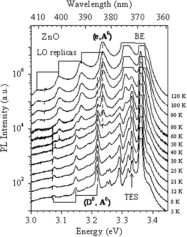
Photoluminescence (PL) spectra of undoped ZnO at different temperatures, showing that between 30 and 100 K, the donor–acceptor pair (DAP) transition at 3⋅220 eV decreases, while the adjacent e–A transition at 3⋅236 eV increases. The plots are vertically shifted for clarity (adapted from Thonke et al. 54 )
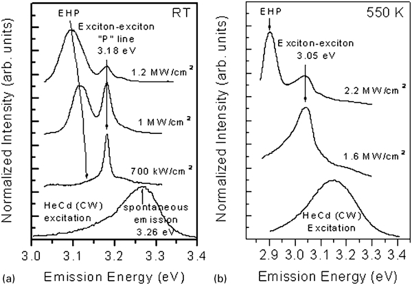
Stimulated emission (SE) is commonly observed from ZnO epitaxial layers. Bagnall et al. 99,100 were the first to show the presence of SE in films grown by MBE. Figure 10 shows the appearance of an electron-hole plasma peak at 3⋅14 eV, which is red-shifted and broadened as the excitation intensity is increased. 100,101 What is needed is to translate this promising optically pumped performance into demonstrations of electrical injection lasing. As mentioned earlier, the PL spectra from ZnO are fairly consistent, with the band-edge peaks and a deep midgap emission band usually present.
Bandgap engineering
There is a strong need for tailoring the optical emission wavelength for solid-state light sources. A crucial step in designing modern optoelectronic devices is the realisation of bandgap engineering to create barrier layers and quantum wells in device heterostructures, which have the necessary optical and carrier confinement to realise efficient light emission. An example of such a heterostructure based on ZnO is shown in Fig. 11. In order to realise such optoelectronic devices, modulation of the bandgap is required. The emission wavelength of the ZnO can be tuned over a broad range by alloying with Cd or Mg. This has been demonstrated by the development of MgxZn1−xO and CdyZn1−yO alloys, allowing bandgap tuning in a wide range. Figure 12 shows the a-axis lattice constants and bandgaps of CdyZn1−yO and MgxZn1−xO as a function of a-axis lattice constant and bandgap, along with similar data for the AlInGaN system. 98
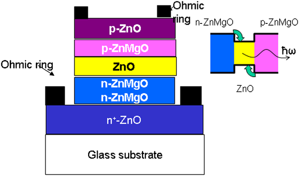
Schematic of double heterostructure using a ZnO active region and ZnMgO cladding layers
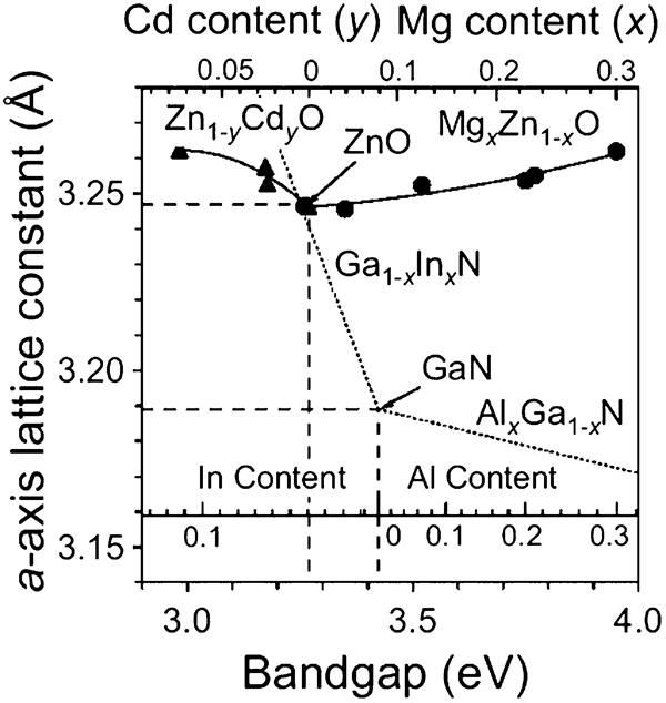
Optical and structural properties of CdyZn1−yO and MgxZn1−xO as a function of a-axis lattice constant and bandgap. Similar data for InGaN and AlGaN are also shown (adapted from Ozgur and Morkoc 98 )
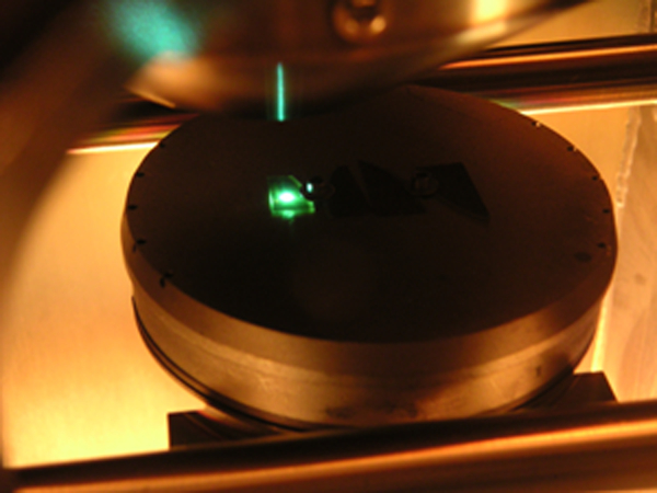
For light emitters, an attractive approach is the use of a ZnCdO active region with ZnMgO clad layers to form a double heterostructure. The band offsets for ZnMgO and ZnCdO with ZnO at fixed compositions of 5% Cd are shown in Fig. 13 and 10% Mg in Fig. 14, respectively, using X-ray photoelectron spectroscopy. For ZnMgO, the band offset is predominantly in the valence band, while for ZnCdO, there is a division of approximately 2:1 between the conduction band offset and the valence offset. There is still a lot of development to be done on the ternary alloys, particularly ZnCdO, where there are solubility limits for Cd incorporation that must be addressed and require low temperature growth with non-equilibrium techniques such as MBE. This technique is capable of producing films with excellent optical quality, as shown in Fig. 15, which demonstrates bright green emission from a ZnCdO sample during excitation with an in situ electron beam. The structural quality of such layers is also high, as shown in the TEM cross section and selected area diffraction pattern in Fig. 16 of this ZnCdO/ZnO structure grown on sapphire substrates.
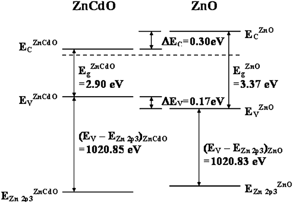
Schematic band diagram for ZnO/ZnCdO with 5% Mg composition
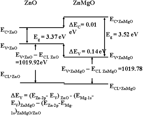
Schematic band diagram for ZnO/ZnMgO with 10% Mg composition
Photograph of green light emission from ZnCdO film during excitation with electron beam
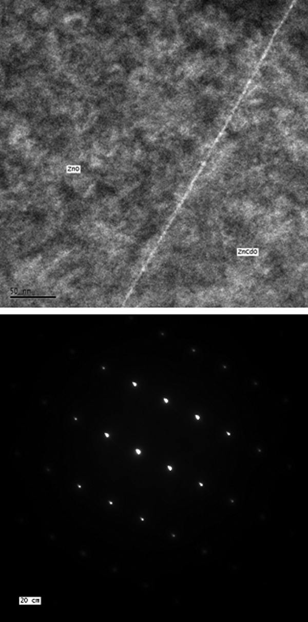
TEM cross section (top) and selected area diffraction pattern (bottom) of ZnCdO/ZnO heterostructure grown by molecular beam epitaxy (MBE)
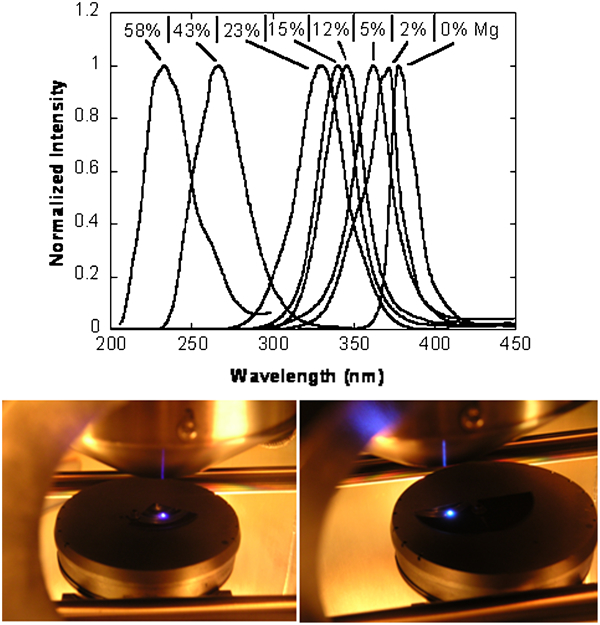
Similar comments apply to ZnMgO samples grown by MBE. As an example, a series of ZnMgO samples were prepared by MBE. Room temperature cathodoluminescence (CL) measurements were performed on the samples to define the spectral position of the near band-edge emission peaks for MgxZn1−xO with different compositions. Using the spectral peak positions, the bandgap energy of the MgxZn1−xO can be calculated and correlated to the overall concentration of Mg in the films. 102 Figure 17 below shows the normalised CL peak intensity of the MgxZn1−xO films and their respective Mg concentrations. Note that there is a gap with 0⋅23<x<0⋅43, where no distinctive CL emission can be measured from the samples, which is in principle consistent with the mixed phase region previously reported. However, the gap should have a lower boundary at x∼0⋅33, which is higher than our result of 0⋅23. This might be due to the inaccuracy associated with the optical method we used to determine the bandgap energy. In order to obtain relatively precise composition data, techniques such as wavelength dispersive spectrometry is currently being employed to measure the Mg concentrations in these films.
Emission wavelengths from ZnMgO layers grown by molecular beam epitaxy (MBE) as a function of composition(top) and blue cathodoluminescence (CL) from single layer ZnMgO (bottom left) and multi quantum well (MQW) (bottom right)
The energy gap E
g(x) of the ternary semiconductors MgxZn1−xO and CdxZn1−xO is determined by the following equations

A (Cd,Zn)O/(Mg,Zn)O SL, having a perfect lattice match between layers and a maximum barrier height of 0⋅09 eV, can be obtained by choosing an appropriate combination of Cd and Mg concentrations, because both a-parameters are monotonically increasing functions of alloy composition. This is a major advantage when compared to (In,Ga)N/(Al,Ga)N SLs since, in the case of wurtzite structure, if the lattice constant of the well layer differs from that of the barrier layer, strain field exists inside the well layers, which causes polarisation charge.
There is a clear need for providing some design parameters for the LED structures in terms of layer structure, doping and composition and how they affect light emission intensity and I–V characteristics. More effort is needed on modelling of band alignment and carrier transport in ZnO-based heterostructures. For example, results from simulations are shown in Fig. 18. Several ZnO-based LED structures were examined using a 1-D simulator that accounts for specific features of the hexagonal semiconductors: strong piezoeffects, existence of spontaneous electric polarisation, low efficiency of acceptor activation, and high threading dislocation density (normally, ∼107–109 cm−2) in the material. The simulation program used was the SiLENSe code. This is a 1-D simulator that can build a band diagram, carrier injection and recombination, and light emission profiles in wide bandgap LED heterostructures. The SiLENSe 2⋅1 version is capable of simulating heterostructures made not only of group III nitrides, but also of other wurtzite semiconductors (for example, ZnMgO alloys) including hybrid structures. The LED operation of the heterostructure is considered within the framework of the 1-D drift diffusion model of carrier transport that accounts for specific features of the wurtzite semiconductors. Along with bimolecular radiative electron and hole recombination, an original model of non-radiative carrier recombination at threading dislocation cores is also considered. The latter allows an analysis of the interaction between the radiative and non-radiative recombination channels and predicts the internal emission efficiency of the LED structure as a function of threading dislocation density. The spectrum of light emission from a single or multiple quantum-well active region can be calculated to account for the complex valence band structure of wurtzite semiconductors using the 8×8 Kane Hamiltonian. Energies and wave functions of localised carrier states are found by a numerical solution of the Schrödinger equation within the effective-mass approximation. Generation of the grid for each QW is totally automated.
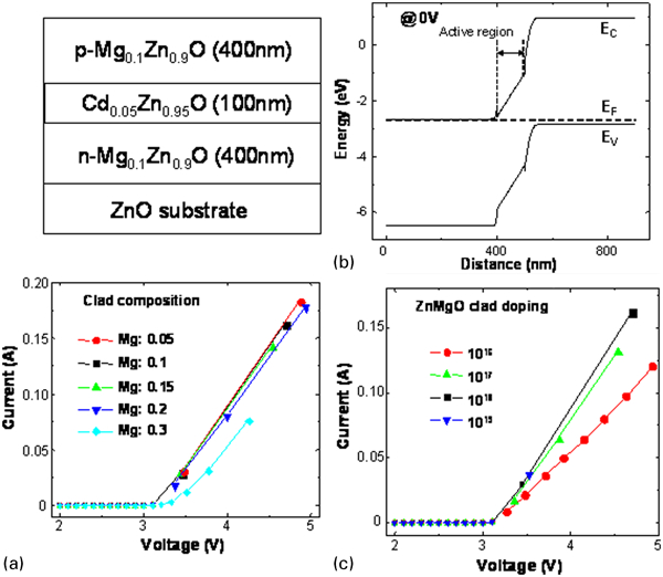
Simulation results for ZnMgO/ZnCdO/ZnMgO heterostructures
The model implemented into the code incorporates the following: (i) localised and distributed polarisation charges in the LED structure induced by both spontaneous and piezo-polarisation in nitride semiconductors; (ii) Fermi statistics for electrons and holes for both degenerate and non-degenerate semiconductors; (iii) partial ionisation of donor and acceptor dependence on the respective quasi-Fermi level positions; (iv) strain calculations in the LED structure assuming coherent growth of all epilayers on an underlying buffer layer; (v) bimolecular radiative electron and hole recombination neglects quantum-confined effects on the recombination rate; and (vi) non-radiative carrier recombination in the principal channel and on threading dislocation cores. The LED I–V characteristics are calculated by the software at a given serial resistance that is assumed to account for both the lateral current spreading in the LED chip and Ohmic contact resistances. Moreover, the light emission spectra are determined with a post-processing module that uses the calculated band profiles of the LED structure and takes into account the complex structure of the valence band of nitride materials and the contribution of the confined electronic states. Simulation results should be used as a guide for identifying important parameters in the LED design rather than as definitive. The simulator gives indicators of the most important design features for a heterostructure ZnO LED.
Fabrication processes for ZnO photonic devices
The fabrication sequence for ZnO LEDs depends on whether a vertical or mesa-type structure is used. If an insulating substrate such as sapphire is used for the growth of the ZnO layers, then both n- and p-type contacts must be made on the top of the structure by forming a mesa to expose the other side of the p–n junction. If, however, a conducting substrate is used, then the n- and p-contacts are made on opposite sides of the entire structure and no mesa formation is needed. This is shown schematically in Figs. 19 and 20. In either case, it is necessary to develop low resistance Ohmic contacts to both conductivity types of ZnO.
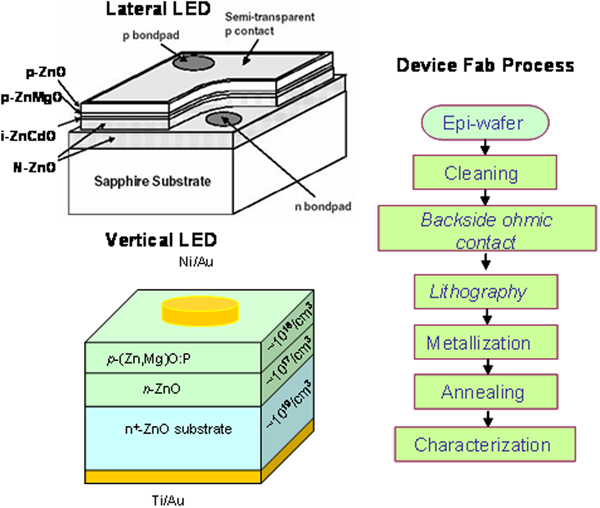
Schematic of lateral (top) or vertical (bottom) light emitting diode (LED) and process sequence for vertical device
Schematic of mesa formation on lateral geometry ZnO/GaN heterojunction light emitting diode (LED)
n-type Ohmic contacts
The achievement of acceptable ZnO device characteristics relies heavily on developing low specific contact resistance Ohmic metallization schemes. 103,104 The usual approaches involve surface cleaning to reduce barrier height or increase of the effective carrier concentration of the surface through preferential loss of oxygen. 105 Specific contact resistances of ∼3×10⁻⁴ Ω cm−3 were reported for Pt–Ga contacts on n-ZnO epitaxial layers, 2×10⁻⁴ Ω cm−3 for Ti/Au on Al-doped epitaxial layers, 0⋅7 Ω cm−3 for non-alloyed In on laser-processed n-ZnO substrates, 2⋅5×10−5 Ω cm−3 for non-alloyed Al on epitaxial n-type ZnO, 7⋅3×10−3–4⋅3×10−5 Ω cm−3 for Ti/Au on plasma exposed Al-doped n-type epitaxial ZnO and 9×10⁻⁷ Ω cm−3 for Ti/Al on n+-epitaxial ZnO. Several points are clear from the past works, namely that the minimum contact resistance generally occurs for post-deposition annealing temperatures of 200–300°C on doped samples, which must be treated so as to further increase the near-surface carrier concentration. Table 3 summarises the results in the literature for n- and p-type Ohmic contacts to ZnO materials. At this stage, the quality of Ohmic contacts to ZnO is acceptable for LED applications, although the contact resistance of p-Ohmics would of course improve if higher hole concentrations could be achieved in P–ZnO.
Ohmic contacts ZnO and their respective specific contact resistance from published works
Light emitting diode results
There are many reports of EL from ZnO structures, though as mentioned earlier, care must be taken to exclude electron-hole recombination in MIS structures where hole generation at grain boundaries can lead to small band-edge peaks being observed. It appears that some of the literature reports may actually be due to this effect rather than to actual electron-hole injection from p–n junctions. Although ZnO-based light emitting devices have been reported using different deposition techniques, the injection efficiencies are very low, mostly due to the poor p-type conductivity in the ZnO layers. When the p-doping concentration is an order of magnitude lower than the adjoining n-type ZnO, helping compose the p–n junction, injection from the highly doped n-type ZnO to the lightly doped p-type ZnO becomes dominant and the recombination takes place primarily in the p-type ZnO. Although this can be mitigated by using a large bandgap p-type material such as MgZnO or BeZnO, the hole concentrations are still low (<1016 cm−3) as well as the poor material quality, degrading the overall recombination efficiency.
The much higher mobility (factor of at least 100) and concentration (more than an order of magnitude) of electrons than holes in ZnO-based LEDs causes electron overflow and increases recombination processes in the p-type ZnO region. Owing to the generally low quality of the p-ZnO, this reduces the radiative recombination efficiency. To help reduce this problem, use of heterostructures is advantageous. Many designs have employed MgZnO as an energy barrier layer to confine the recombination processes to the active layer. These ZnO LEDs typically show enhanced UV emission and suppressed deep level emission. However, the undoped MgZnO layer also decreases the hole transport from p-type ZnO to the ZnO active layer because its large bandgap provides an energy barrier to hole injection. One way to improve hole injection efficiency and the recombination rate in the active layer of LEDs is to use a p-type electron blocking layer (EBL). The hole concentration in the undoped ZnO active layer can be increased because of the lower Fermi energy level in p-type MgZnO compared with undoped or n-type MgZnO. However, the recombination efficiency is still generally very low due to the low achievable hole concentrations in the cladding layers as well as their often poor material quality.
Although the initial results on electrically injected ZnO-based light emitters are encouraging, further improvements in p-type conductivity of ZnO and device processing are necessary for transition to reliable consumer applications, and the progress has been slow. While the efforts on producing conventional edge emitting lasers under electrical injection are hindered by the absence of reliable and high-quality p-type ZnO, optically pumped surface emitting lasers based on ZnO have been attracting a great deal of attention. However, as stated already, high-efficiency light emitting devices cannot be implemented before the fundamental issues related to p-type conductivity in ZnO are resolved. The absence of reliable p-type conductivity prevents ZnO from being even remotely competitive with GaN for optoelectronic applications. There may be applications for ZnO-based low-threshold devices based on polariton lasing in data storage.
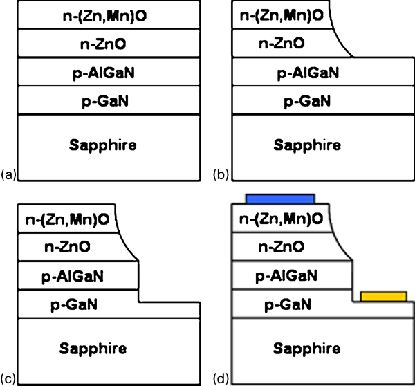
Let us examine some specific examples of ZnO-based LED performance to give a better picture of their limitations. The first is that of ZnO/GaN heterojunction LEDs, which substitute p-GaN as the source of holes. 80 An optical image of such a device is shown in Fig. 21. The entire structure was grown by MBE. In this case, the top ZnMgO layer is partially removed by wet etching to expose the underlying p-GaN. Electroluminescence spectra from the device as a function of temperature are shown in Fig. 22. A significant red shift in the emission peak to 401 nm occurs at T = 650 K for a current of 160 mA. The origin of the optical emission may be the annihilation of free or bound excitons, as suggested by optical absorption, photocurrent and CL spectral measurements. The red shift is similar to that reported by Tsukazaki 24 in their devices. Similar to the rectifying I–V characteristics, the EL emission was observed up to 400°C, the temperature limit of the heating stage used in our experiments. The optical power measured at room temperature from a test device mounted on a header was ∼10 μW at room temperature. The power was measured using a wrap-around geometry that gives consistent measurement of the total output power. Optical emission power, measured at 22, 220 and 370°C, increased linearly with forward current over a large range of currents. Light emission currents at which light was detected by the spectrometer for 22, 220 and 370°C were I 22 = 7⋅8, I 220 = 48, and I 370 = 54 mA, respectively. The light emission intensity was low for current values below the threshold. Presumably, the non-radiative recombination was a predominant mechanism responsible for transitions in this structure below the threshold current values. The linearity of the optical power dependence above the threshold provides additional evidence that the optical emission is interband-related rather than impurity-related. Electroluminescence spectra measured at T = 220°C for different pulse driving currents are shown at the bottom of Fig. 22. The pulse width used for this experiment was 200 μs, which also contributed to the heating of the devices at the duty cycle of 10%. The emission band with a peak at ∼390 nm originates from the near-interband transition in the ZnO active region near the p-AlGaN interface. The forward I–V characteristics as a function of temperature are shown in Fig. 23 (note that the threshold voltage does not degrade significantly over the range 200–320°C). These LEDs show a wide range of operating temperatures, with strong UV emission originating from excitonic transition in ZnO observed up to 370°C. However, they do not offer any particular advantage over more established GaN-based LEDs and the fact that p-GaN is needed removes the rationale for this approach. Generally, a comparison of EL and PL spectra of n-type ZnO and p-type GaN layer in these structures shows two EL emission peaks attributed to radiative recombination in both n-type ZnO and p-type GaN layers.
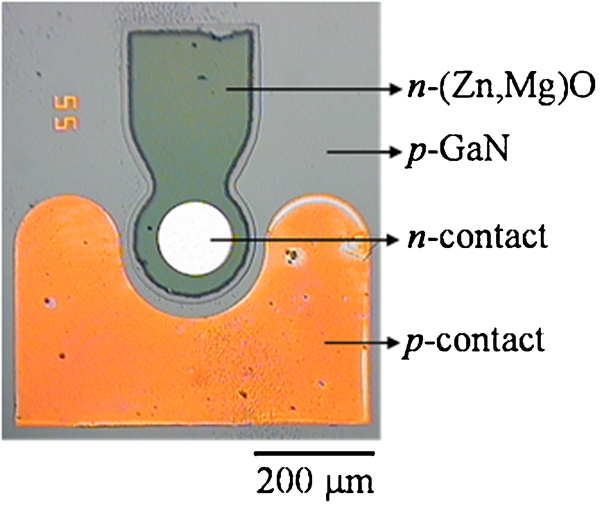
Photograph of completed ZnO/GaN light emitting diode (LED) structure
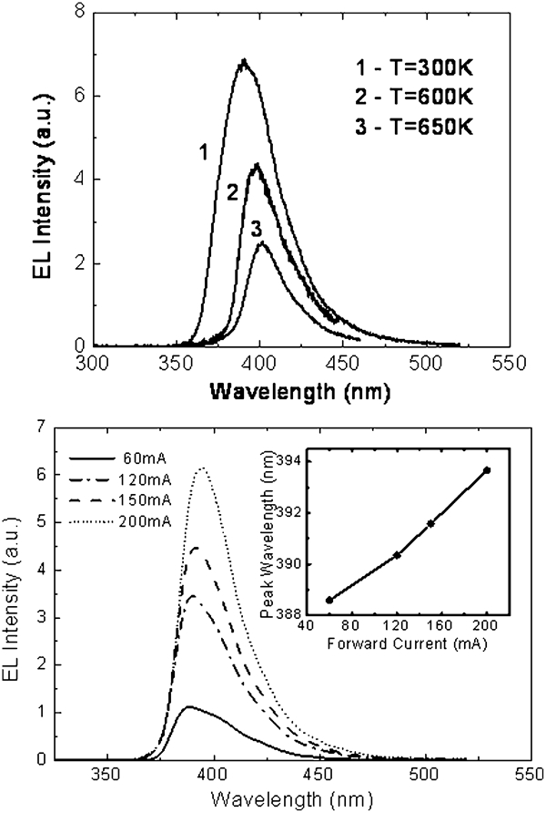
Electroluminescence (EL) as a function of operating temperature (top) and drive current (bottom) from hybrid ZnO/GaN light emitting diode (LED) (adapted from Ref.88)
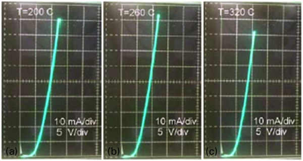
Forward I–V characteristics from hybrid ZnO/GaN light emitting diode (LED) as a function of operating temperature
Examples of the structure and performance of homojunction ZnO LEDs are shown in Fig. 23. 25,86 This structure was grown on a ScAlMgO4 substrate by MBE. The threshold voltage of about 7 V is higher than the expected value of around 3⋅3 V owing to the high series resistance of the p-ZnO and the EL spectrum shows interference fringes from multiple reflections. The band-edge to deep level emission ratio is low and ideally would be >100.
A novel heterostructure design is shown in Fig. 25, employing ZnBeO cladding layers for improved carrier confinement, with Be0⋅3Zn0⋅7O layers and BeZnO/ZnO quantum-well active layer between n-type and p-type ZnO. 83 Arsenic was used as the acceptor dopant and a hybrid approach combining PLD, MBE and CVD was employed for the growth. 84 Figure 25 shows the layer structure, EL spectra as a function of drive current and the I–V characteristics. The peaks located near 388 nm (bound exciton) and 550 nm (green band) are the dominant features at low forward currents. The primary spectral emission peak is located near 363 nm and arises from localised exciton emissions in the QWs. The secondary peak centred near 388 nm is from impurity-bound exciton emissions in ZnO. The blue shift of the peak at 550 nm as current injection is increased indicates impurity-involved emission such as from DAP recombination. Overall, the performance of the LED is mediocre when compared to GaN devices and the growth approach not readily applied to mass production.
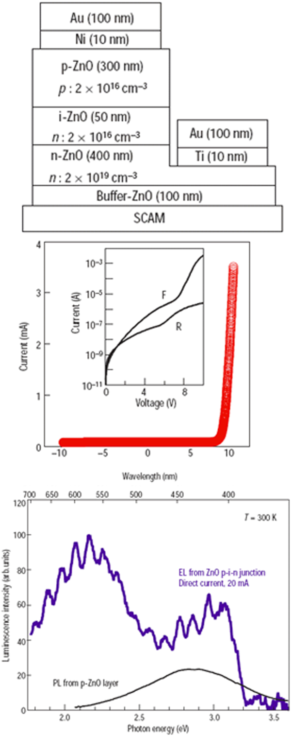
Schematic (top), I–V (centre) and electroluminescence (EL) and photoluminescence (PL) spectra (bottom) from ZnO homojunction (adapted from Ref.24)
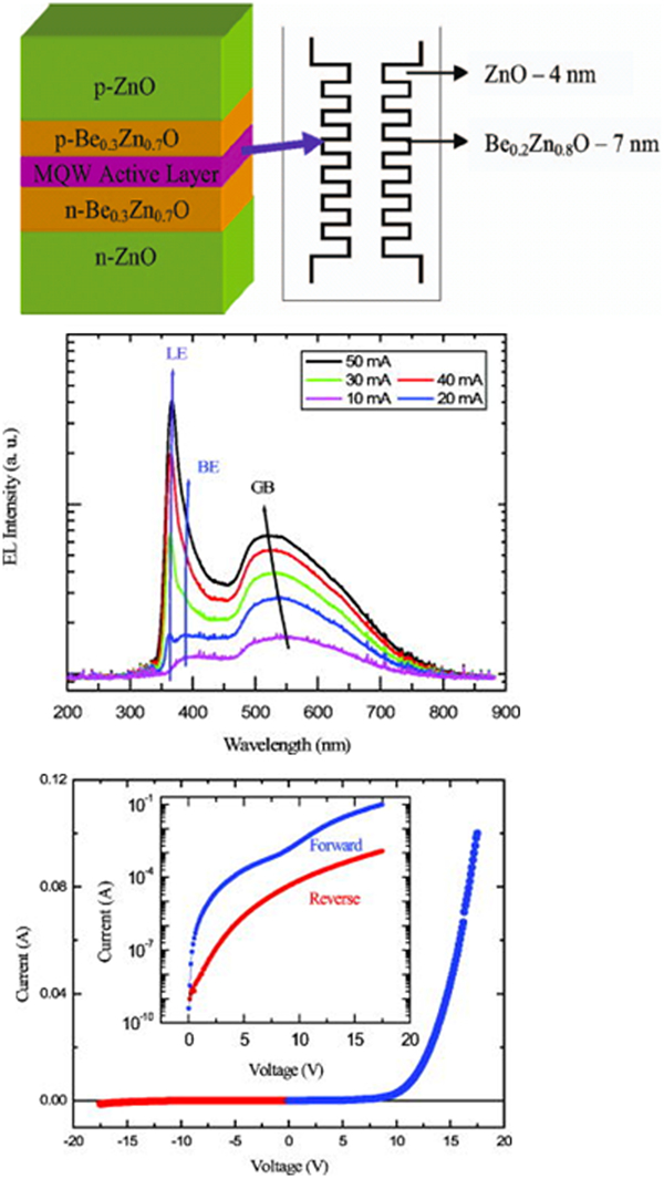
Schematic (top), I–V (centre), electroluminescence (EL) spectra (centre) and I–V characteristics from ZnO/ZnBeO heterojunction (adapted from Ref. 92)
As a final example, Fig. 26 shows a structure involving ion implantation of n-ZnO substrates with N in an attempt to create a surface p-layer. Ion implantation is an attractive process for low-cost, high throughput device manufacturing. However, while N+ implantation into bulk single-crystal ZnO substrates can be used to achieve band-edge EL in simple diode structures, the mechanism for band-edge EL is most likely hole creation by impact ionisation in the MIS structure. 106,107 The devices do show visible emission and a small band-edge peak at low temperatures, but there was no evidence for the creation of a p-layer and it was suggested that the role of the N+ implantation and subsequent anneal was to create a resistive layer that leads to the realisation of an MIS diode upon metallization. As we discussed earlier, Mahan et al. 21 in presenting a theory to explain the conduction in ZnO-based metal-oxide varistors, suggested that holes could be created by impact ionisation during biasing. Direct evidence of the production of holes in forward-biased ZnO varistors was later reported by Pike et al. 20 with the detection of band-edge EL in addition to the broad subband-gap luminescence that peaked near 600 nm.
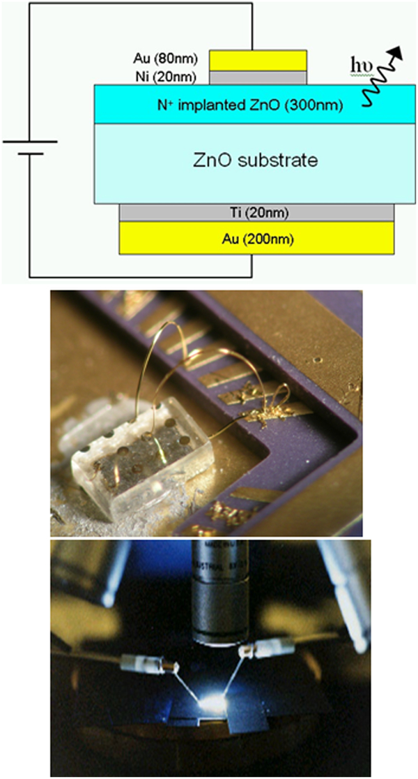
Schematic (top), photograph of completed device (centre) and emission (bottom) from N ion implanted ZnO structure (adapted Ref. 119)
While ZnO LEDs are plentiful, true electrically pumped lasing in a real laser diode remains elusive. The reports of lasing to date are optically pumped surface emitting structures, usually operating below room temperature, with an emphasis on polariton lasers with ZnO microcavities. 108–113 At this point, these are far from having any impact on existing visible laser diode applications. High-efficiency light emitting devices cannot be implemented before the fundamental issues related to p-type conductivity in ZnO are resolved. Unavailability of reliable p-type conductivity prevents ZnO from competing with GaN for optoelectronic applications at present. It is, however, clear that ZnO-based low-threshold or nearly thresholdless lasers, especially those based on polaritons, may be feasible.
Comparison with GaN light emitters
As a comparison of the relative efficiencies of ZnO LEDs at this point, which are generally less than 1%, Fig. 27 shows data for InGaN and AlGaInP visible LEDs. 4 Note the region in the wavelength spectral window from ∼530 to 570 nm, known as the ‘green gap’. In this wavelength range, it has proven difficult to produce efficient green LEDs. Since current white light generation techniques relies on colour mixing from red, blue and green LEDs, availability of an efficient green LED would be a major breakthrough. For GaN LEDs, alloy phase separation occurs when large amounts of In are added to GaN to shift the emission into the green gap, or Ga is added to the InN to shift the emission towards the red. However, even with the reduced efficiency of both conventional materials systems in this green gap region, the existing ZnO LEDs would show effective external quantum efficiencies of zero on Fig. 27.
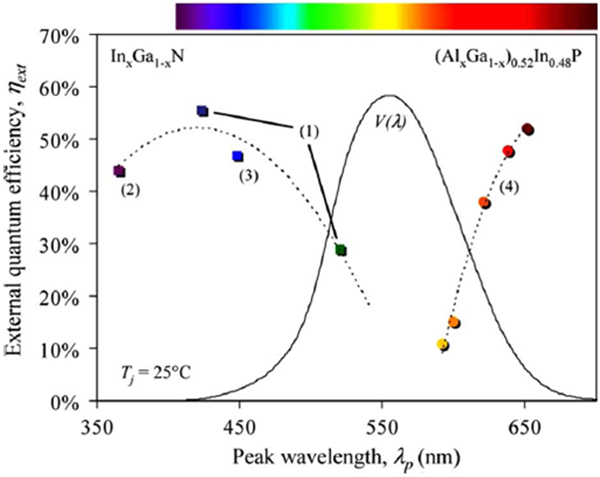
External quantum efficiency for visible GaN- and AlGaInP-based light emitting diodes (LEDs). The numbers refer to various compositions of InGaN and AlGaInP production LEDs. The curve labelled V(λ) is the luminous eye response curve derived from the CIE (Commission Internationale de l’Eclairage) colour space diagram (adapted from Ref. 4)
Two processes occur in the semiconductor: generation and recombination. Generation occurs when the energy of carriers in the semiconductors is raised above their equilibrium and a pair of an electron and a hole generate. After the carriers having lived a mean lifetime in the higher energy state, they give their energy as spontaneous emission of photons or phonons. While the exciton binding energy of ZnO is higher than for GaN, the lack of robust p-type doping, poor control of surface conductivity and interface quality, presence of compensating donors and lack of basic understanding on the role of polarity have all contributed to the lack of progress relative to GaN for LEDs. Although the internal quantum efficiency has been improved by advances in epitaxial growth techniques, the methods used to extract the photons from the active regions still need to be improved. The following is a list of areas where work is need in ZnO growth and characterisation in order to improve LED efficiency and reproducibility.
better understanding of minority carrier injection across heterojunctions
better understanding of dopants and defects
location of dopants in lattice
role of hydrogen in compensating acceptors or in enhancing incorporation of acceptors
better understanding of ZnO, ZnMgO epitaxy (is non-equilibrium growth needed for high acceptor incorporation?)
growth on alternative orientations of sapphire
change in growth morphology with orientation
role of polar/nonpolar interfaces
heterostructure growth on single-crystal ZnO substrates
nucleation for homoepitaxy; characterisation of substrate surface
In solid-state lighting, the present research focus is on increasing the photon flux per package. The photon flux φ (in units of lumens) is given by the relation
Figure 28 shows a list of areas related to the growth of ZnO-based LED structures that need additional research in order to enhance the radiative efficiency of the unpackaged devices. At this point, however, unless there is a significant breakthrough in achieving higher p-type doping levels, most of these areas are more of fundamental interest than likely to move ZnO light emitters into commercially availability.
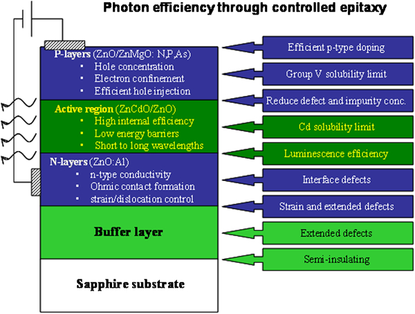
Required improvements needed for efficient ZnO-based light emitters
Conclusions
Most semiconducting oxides are ‘natively’ n-type and it is difficult to achieve reproducible and stable p-type doping. The background n-type conductivity is often ascribed to intrinsic point defects, but in some cases, residual impurities can play a role, emphasising the need for more focus on high purity growth techniques. One fundamental reason for the prevailing n-type conductivity in ZnO is that the valence band is mostly composed of oxygen 2p orbitals, which have low absolute energy, in this case leading to a valence band maximum 3 eV lower than in Si. Achieving efficient p-type doping requires a low absolute energy for the shallow acceptors and suppression of compensation mechanisms promoted by the large lowering of the electron energy. There is beginning to emerge a better understanding of the limitations of past results on p-type doping of ZnO using the most common dopants, namely N and the group V elements P, As and Sb. Many of the previous claims of p-type doping appear to be dubious based on the reported mobilities and low emission efficiency of LEDs fabricated on these layers. Renewed efforts on reducing the background n-type conductivity are needed, as was the case with GaN materials development. More attention needs to be paid to optimising the buffer layers and crystal quality of ZnO heterostructures intended for LED fabrication and this should emphasise the use of MBE and MOCVD growth methods, which allow for better stoichiometry control and higher purity. 119 The sensitivity of ZnO surfaces to adsorbed gases, in particular oxygen and water vapour, needs to be more widely recognised and accounted for in Hall measurements of p-type layers.
The future for commercial ZnO light emitters appears to be limited unless there are significant breakthroughs in the growth of heterostructures. In the near future, the best approach may be a continued effort on epitaxial growth of these materials, leading to a better understanding of dopant incorporation and defect control.
Footnotes
Acknowledgements
This work is partially supported by the National Science Foundation (J. M. Zavada) under grant 1159682.