
Abstract
Cu–Ni–Si alloys with four different Cu contents were fabricated by means of smelting. Subsequently, isothermal aging and hot rolling followed by aging treatment were carried out. The microstructure and phase composition were characterised by optical microscope, transmission electron microscope and X-ray diffractometer. Electrical conductivity was measured by using an eddy current based technique. The results show that the electrical conductivities of as cast Cu–Ni–Si alloys decrease obviously with a decline in Cu content. Isothermal aging is favourable to enhance the electrical conductivities of Cu–Ni–Si alloys with higher than 90Cu content rather than that with <90Cu content containing an integrated netted structure of grain boundary phases. The electrical conductivities of as rolled Cu–Ni–Si alloys can obviously be increased by subsequent aging treatment. The above results suggest that the disintegration of the integrated netted structure at the grain boundary is a promise to achieve high electrical conductivity for Cu–Ni–Si alloys.
Introduction
Owing to the excellent electrical and thermal conductivities, pure copper and its alloys are now being used widely in electrical power, electronics and instrumentation applications.1–3 However, the rather low tensile strength limits their utilisation as industrial materials.4Therefore, it is an interesting question of how to improve the tensile strength while retaining the attractive electrical and thermal conductivities of pure copper and its alloys.
Cu–Ni–Si alloys are mainly strengthened by high temperature quenching and subsequent heat treatments, resulting in the precipitation of δ-Ni2Si phases in the copper matrix and the improvement of tensile strength.5–10However, the mechanical properties and the electrical conductivity of as cast copper alloys are not only controlled by heat treatments but also by alloying composition. For example, Cu–Ni–Si system alloys with higher Cu content usually present good electrical conductivity and reasonable strength and can be used as conducting wires,11whereas alloys with lower Cu content possess greater strength and meaningful electrical conductivity and can be used as contactors.12–14Until now, some efforts have been made to develop a series of Cu–Ni–Si alloys, where the addition of Ni and Si elements is commonly <5 wt-. Although their electrical conductivity can be as high as 58 according to the International Annealed Copper Standard, their strength is always <600 MPa.5–10
In order to achieve stronger strengthening, higher Ni and Si addition into Cu–Ni–Si alloys is necessary, and their solidification behaviour has also been investigated systemically in our previous work.15 It was noticed that with increasing Ni and Si addition, large numbers of netted structure identified as eutectic products formed at the grain boundary. Up to now, there is still no literature to report the influence of such a netted structure on the properties, especially on the electrical conductivity of Cu–Ni–Si system alloys. The purpose of the present paper is to investigate systemically the relationship between the netted structure and the electrical conductivity of Cu–Ni–Si alloys.
Experimental
As cast Cu–Ni–Si alloys were prepared by in situ alloying from 99·9 wt- pure Cu, 99·9 wt- pure Ni and 99·9999 wt- pure Si using a medium frequency induction furnace. The atomic ratio of Ni/Si in as cast Cu–Ni–Si alloys was 3∶1, and the Cu contents were 95, 90, 80 and 60 wt- respectively. In the course of smelting and pouring, graphite crucible and mould were used, and the preheating temperature of the graphite mould was 400±10°C. The ingots were quenched rapidly into water immediately once they solidified.
Isothermal aging of as quenched Cu–Ni–Si samples was carried out in an electrical resistance furnace, where the temperature was ∼450°C, and the times were 0·5, 2, 4, 6 and 8 h respectively. After aging for a given time, the samples were cooled in air.
The ingot with a dimension of 80×12×12 mm was hot rolled to a plate with a dimension of 240×15×3 mm in the temperature range from 1000 to 850°C. Subsequently, these as rolled samples were aged at 450°C for 8 h and then cooled in air. For the sake of convenience, such a treatment was referred as hot rolling+aging in the following text.
All the samples were cut along the transverse direction, polished and then etched with 8 g FeCl3+20 mL HCl+100 mL H2O solution. The microstructure was observed by optical microscope (Olympus GX71) and transmission electron microscope (JEM 3010). The electrical conductivity was measured at room temperature first using an eddy conductivity apparatus (7501) and then transformed into relative electrical conductivity according to the International Annealed Copper Standard, where the values were the average value of five tests. An X-ray diffractometer (7000) was employed to confirm the phase composition of Cu–Ni–Si alloys, where the scanning speed was 10° min−1, the work voltage is 40 kV, the current is 50 mA and Cu is used as target.
Results
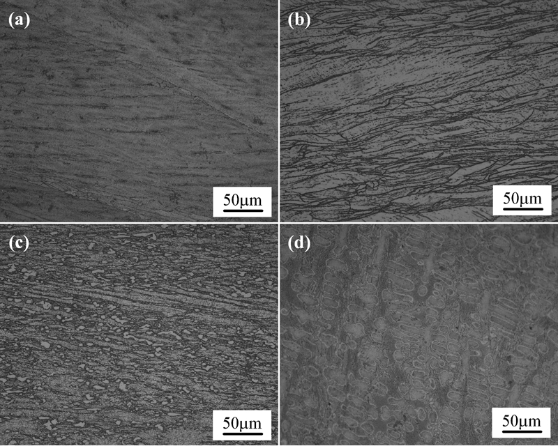
Figure 1 presents the microstructures of as cast Cu–Ni–Si alloys with different Cu contents. Our previous work15 suggested that the phase composition of such four Cu–Ni–Si alloys composed of three phases, including solid solution phase α-Cu(Ni,Si), eutectic phase α-Cu(Ni,Si)+Ni3Si at the grain boundary and acicular phase δ-Ni2Si in the α-Cu(Ni,Si) phases. Considering δ-Ni2Si phases to be inhibited by rapid water quenching, it is hence thought that there are only two phases, i.e. solid solution phase α-Cu(Ni,Si) and grain boundary eutectic phase α-Cu(Ni,Si)+Ni3Si occurring in as cast Cu–Ni–Si alloys, as shown in Fig. 1. With a decline in Cu content, the amount of grain boundary phases increases remarkably. As the Cu content declines from 90 to 80, a discontinuous structure of grain boundary phase transfers into a continuous one. The larger the addition of Ni and Si, the better the integrality of the netted structure (Fig. 1c and d).
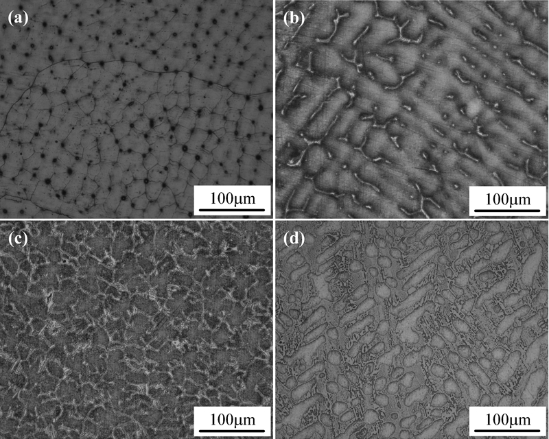
Microstructure of as cast Cu–Ni–Si alloys with a 95, b 90, c 80 and d 60Cu respectively
For such four as cast alloys, the testing results of electrical conductivities are shown in Fig. 2. On the whole, the electrical conductivities of Cu–Ni–Si alloys decline monotonously with decreasing Cu content. The change of electrical conductivity against Cu content can obviously be divided into three different stages. Comparatively, the decline in electrical conductivity in the second stage is the most significant, corresponding to the formation of a netted structure at the grain boundary when the Cu content decreases to 80 (Fig. 1c and d). Therefore, it is reasonable to believe that for Cu–Ni–Si alloys with higher Ni and Si additions, the decline of electrical conductivity correlates closely with such an integrated netted structure at the grain boundary.
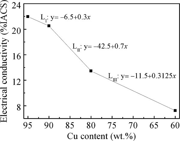
Electrical conductivity versus Cu contents of as cast Cu–Ni–Si alloys
In order to enhance the electrical conductivity of as cast Cu–Ni–Si alloys, a relevant aging treatment was carried out, and the corresponding result is shown in Fig. 3. It can be noticed that, except for Cu content higher than 90 wt-, the electrical conductivity of Cu–Ni–Si alloys seems to be steady with a prolongation of time. It can be seen from Figs. 4 and 5 that the microstructure change of Cu–Ni–Si alloys can mainly be characterised by the precipitation of δ-Ni2Si phases, while the netted structure at the grain boundary do not change before and after aging treatment (Fig. 4d). Obviously, it is favourable for the aging treatment to precipitate δ-Ni2Si phases in α-Cu(Ni,Si) phases, but unprofitable to change the integrated netted structure in Cu–Ni–Si alloys with <90Cu content (Fig. 4c and d). Therefore, it seems to further suggest that the electrical conductivity might be controlled by the integrated netted structure of the grain boundary phase in Cu–Ni–Si alloys with <90Cu.
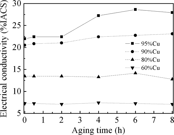
Electrical conductivities of Cu–Ni–Si alloys with different Cu contents after aging at 450°C for different times
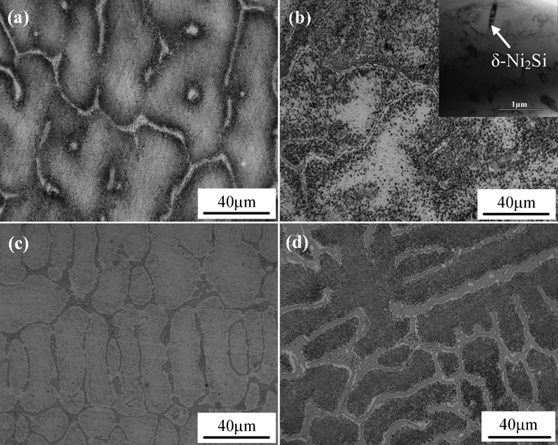
Microstructures of two Cu–Ni–Si alloys in different states
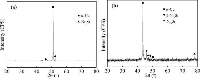
X-ray diffractometer patterns of Cu–Ni–Si alloys with 90Cu content
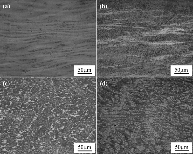
Considering the effect of the netted structure, a hot rolling treatment was carried out. It can be seen from Fig. 6 that the integrated netted structure in as cast Cu–Ni–Si alloys is destroyed, and an obvious rolling texture can be observed. Accordingly, the microstructure of the hot rolling+aging samples is shown in Fig. 7. Combining Fig. 6 with Fig. 7, there are almost the same morphologies found in the microstructure of as rolled Cu–Ni–Si alloys before and after aging, and the only difference is that there are large numbers of δ-Ni2Si phases precipitated in the as rolled Cu–Ni–Si alloys after aging, especially in Fig. 7c.
Microstructures along transverse direction of Cu–Ni–Si alloys with a 95, b 90, c 80 and d 60Cu after hot rolling
Microstructures along transverse direction of Cu–Ni–Si alloys with a 95, b 90, c 80 and d 60Cu after hot rolling+aging
The electrical conductivities of all the Cu–Ni–Si samples in the different states are charted in Fig. 8. It is found that the electrical conductivities of the four alloys decreases slightly after hot rolling alone, resulting from the decomposition of δ-Ni2Si phases in as cast alloy at a hot rolling temperature ranging from 1000 to 850°C. However, it is surprising that the electrical conductivities of Cu–Ni–Si alloys with <90Cu are obviously enhanced by hot rolling+aging (Fig. 8). Such a result is a strong support for the fact that the integrated netted structure at the grain boundary has an obvious influence on the electrical conductivity of Cu–Ni–Si alloys.
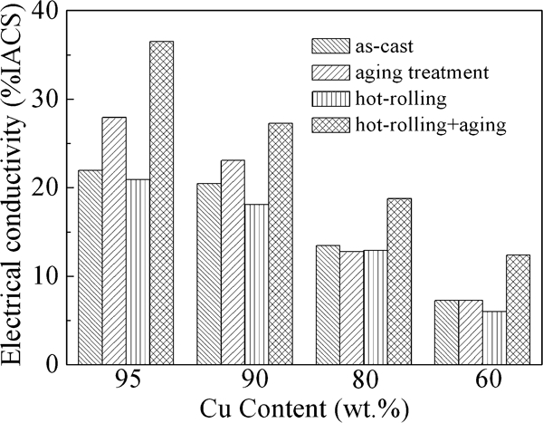
Electrical conductivities of Cu–Ni–Si alloys after different treatments
Discussion
For the alloys or composites, the total electrical resistivity can be expressed as follows16

For high Ni and Si addition, the netted structure of the grain boundary phases is so integrated that the electrons will be difficult to get across the grain boundary phases with poor electroconductibility. In spite of aging treatment, the integrality of the netted structure has not yet been changed, and the improvement of electrical conductivity caused by the precipitation of δ-Ni2Si phase will be restrained. Hence, equation (2) will be no longer suitable for Cu–Ni–Si alloys with <90 wt-Cu content before hot rolling. Nevertheless, the improvement of electrical conductivities with high Ni and Si addition agrees well with the result of equation (2) when the integrated netted structure of the grain boundary phases is fully destroyed by hot rolling. Based on the above results, it can be concluded that the netted structure of the grain boundary phases plays a very important role on the electrical conductivity of Cu–Ni–Si alloy with high Ni and Si addition. From the viewpoint of the experiment, it is also considered that the improvement of the electrical conductivity can be actualised by hot−rolling+aging treatment, suggesting that the disintegration the integrated netted structure of grain boundary phases in the as cast Cu–Ni–Si alloys with higher Ni and Si addition is a promise to achieve high electrical conductivity.
Conclusions
The fact that the electrical conductivity of as cast Cu–Ni–Si alloys decreased obviously with a decline of Cu content suggests that the electrical conductivity correlates closely with the integrated netted structure at the grain boundary. Aging treatment is favourable for the precipitation of δ-Ni2Si phases, but it is indeed unprofitable for the disintegration of the integrated netted structure at the grain boundary, resulting in the electrical conductivities of Cu–Ni–Si alloys with <90Cu not to increase. The hot rolling+aging results show that the electrical conductivities of Cu–Ni–Si alloys with lower Cu content can be enhanced evidently when the integrated netted structure at the grain boundary is destroyed. The above results argue that the netted structure of the grain boundary phases plays a very important role on the electrical conductivity of Cu–Ni–Si alloy, especially that with <90 wt-Cu content. It can also be considered that the improvement of the electrical conductivity can be actualised by hot rolling+aging, which suggests that the disintegration the integrated netted structure at the grain boundary in as cast Cu–Ni–Si alloys with higher Ni and Si addition is a promise to achieve high electrical conductivity.
Footnotes
Acknowledgements
The authors are grateful to the Outstanding Doctoral Dissertation Foundation of Xi'an University of Technology (grant no. 101-2111004), the National Nature Science Foundation of China (grant no. U1034002), the Shaanxi Educational Official Scientific Research Foundation (grant no. 07JK350), the opening foundation of the State Key Laboratory of Solid Lubrication, Lanzhou Institute of Chemical Physics (grant no. 0601) and the Shaanxi Provincial Project of Special Foundation of Key Disciplines for financial support.