
Abstract
Ball milling, as a surface nanocrystallisation method, was employed to investigate the influence of severe plastic deformation on the carburisation treatment performed on low carbon steel. The results indicated an enhancement in the carburisation efficiency as a result of surface milling. This enhancement was attributed to the formation of a nanocrystalline layer in the surface of the treated samples. It was found that the main reasons for the accelerated kinetics of the carburisation process would be the considerable amounts of non-equilibrium defects and the finer austenite grains in the early and later stages of the treatment respectively, which facilitate the carbon diffusion.
Introduction
Surface modification has always been considered as an important treatment for achieving optimised properties and enhancing the overall performance of materials. Recently, surface nanocrystallisation has been under consideration due to the unique properties of the nanostructured materials.1 Various novel methods, such as surface mechanical attrition treatment,2 ultrasonic shot peening and high energy shot peening methods,3,4 air blast shot peening,5,6 ball drop method,7 sandblasting and grit blasting,8,9 wire brushing,10 high speed drilling and cutting11,12 and fast multiple rotation rolling,13 have been developed to produce nanostructured layers on the surface of materials.
Although ball milling (BM) is a very commonly used method for the synthesis of nanocrystalline and ultrafine grained structures in powder materials,14 it has not attracted particular attention for producing nanocrystalline regions in bulk materials so far. In the present work, due to the availability and convenience of the technique, BM was employed to create localised plastic deformation on the surface of the samples. The plastic deformation induces grain refinement and significantly enhances the amount of non-equilibrium defects in the surface layers of materials.15
It is clear that grain refinement enhances atomic diffusivity, since grain boundaries act as high diffusion paths.16,17 For this reason, nanocrystalline materials with large numbers of grain boundaries and various kinds of non-equilibrium defects show greatly higher diffusion rates in comparison to their conventional coarse grained counterparts.18 For instance, enhanced diffusion rates for N,19–21 Cr,22 Fe23 and Ni24 in the samples with nanocrystallised surface structures have been reported. Likewise, it can be anticipated that a change in the surface microstructure as a result of plastic deformation would affect the subsequent carburising treatment in view of the fact that the mentioned treatment is a kind of diffusion controlled phenomenon.
The main objective of the present work was to investigate the influence of a prior BM on the subsequent carburising treatment. Furthermore, it was attempted to find a correlation among the prior surface milling, microstructure of the base material and efficiency of the final carburising treatment.
Experimental
The material used in the present work was a Fe–0·15wt-C steel (Fe–0·157C–0·567Mn–0·265Si–0·05Ni). The steel specimen was first annealed at 1100°C for 60 min. Disc shaped samples with a diameter of 24·3 mm and a thickness of 5·2 mm were then machined from the original steel specimen. An especially designed sample holder was employed to fix the sample at the bottom of the milling chamber.
The milling treatments were carried out at room temperature and in an ambient atmosphere for different periods of time (6, 12 and 18 h) using a conventional planetary ball mill with the speed of 250 rev min−1. The diameters of the balls were the combination of 8, 10 and 12 mm. Fifteen balls of each size were used.
In order to investigate the effect of prior surface milling on the carburisation efficiency, three different carburising conditions were chosen. The conditions were as follows: (1) 120 min at 850°C; (2) 120 min at 800°C; and (3) 15 min at 800°C. For solid carburising, the samples were packed in cylindrical boxes, 6 cm in diameter, 15 cm in length and 6 mm in thickness. These boxes were filled with a solid carburising mixture consisting of 90 wood charcoal and 10 barium carbonate.25 The case depths of the samples were measured by microscopic examinations according to method B of ASTM standard G79-83.
Sample preparation was carried out according to ASTM E3 for microhardness investigations and microstructural observations. Automatic processing of images was performed by Clemex Vision System (Clemex Technologies Inc., Canada) and MIP Microstructural Image Processing Software (Nahamin Pardazan Asia, I. R. Iran). A Buehler Micrometer 2100 was employed for microhardness experiments. Microhardness conditions were set to a 9·8 N load for 15 s.
To reveal the primary austenite grain boundaries, the samples that had been carburised at 850°C were embrittled for 16 h at 510°C. After preparation and polishing, they were etched in boiling saturated aqueous picric acid for 35 s and lightly repolished.26
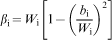
Surface characterisation of the milled samples was performed using X-ray diffraction (XRD) with Cu Kα radiation in a Bruker AXS D8-Advance X-ray diffractometer, a scanning electron microscope (SEM, Tescan Vega) and a field emission SEM (FE-SEM, Hitachi S-4160). The average grain size and mean microstrain of the samples were calculated from the line broadening of bcc Fe (110), (200), (211), (220) and (310) Bragg diffraction peaks using the Scherrer–Wilson method.27 For instrumental correction, an unmilled sample was used as the standard sample (strain free with fully grown grains). The intrinsic profile was obtained using the parabolic equation
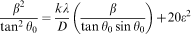
After obtaining the intrinsic profile, the Cauchy–Gaussian relationship (based on integral breadth analysis) was applied for determining the crystallite size and structural microstrain of surface layers in which the lattice microstrain and nanograin are denoted by Gaussian and Cauchy broadening respectively
Results and discussion
The cross-sectional SEM images of the ball milled samples are shown in Fig. 1. A distinct region with a great amount of plastic deformation formed as a result of milling can be recognised close to the surface. In this region, the lamellar structure of pearlite disappeared somewhat through the heavy deformation, and thus, the microstructure consists of accumulated deformed layers of supersaturated ferrite. The formation of a darker layer close to the surface is due to a severe reduction in grain size at those regions. In previous relevant studies, such dark layers were reported as nanostructured zones.7,28,29 The occurrence of severe plastic deformation (SPD) was also confirmed by the microhardness measurements. In Fig. 1d, the presence of wavy bands is obvious; this microstructure is similar to that of powder samples produced from the milling process and believed to be a nanostructured zone.29
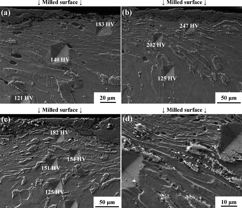
Cross-sectional SEM observation of Fe–0·15C sample after milling for a 6 h, b, d 12 h and c 18 h
Figure 2 shows an FE-SEM image of the underlying layer (∼ 25 μm deep from the top surface) in the sample milled for 6 h. This figure represents very fine grains <100 nm on average, confirming that the thickness of the nanostructured surface layer is not < 25 μm.
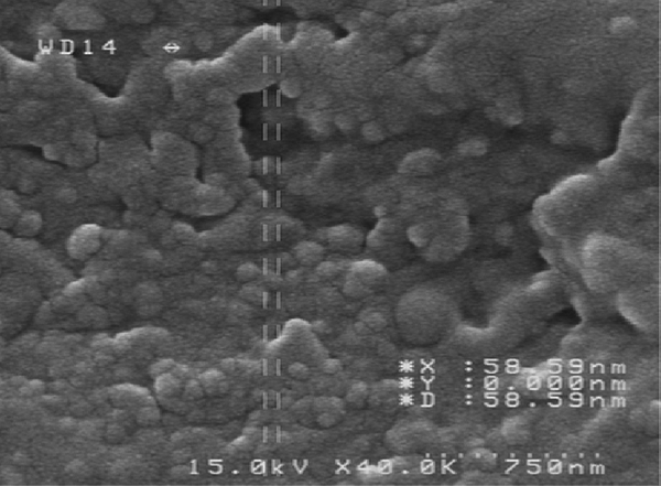
Image (FE-SEM) of sample milled for 6 h (∼25 μm deep from top surface)
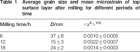
The XRD patterns of the top surface layers before and after the milling are shown in Fig. 3. There is evidence of broadening of the peaks, which can be attributed to the crystalline imperfections induced by the small grain size and microstrain. The structural parameters obtained from the XRD patterns using Cauchy–Gaussian relation are listed in Table 1. It is clear that the average grain size in the top surface layers is in the nanosize regime, which was also verified by FE-SEM studies. The minimum of the average grain size was found to be ∼15 nm after milling for 12 h. In Fig. 1, it can also be seen that the hardness of the surface layers reaches a maximum value (∼250 HV) for the sample milled for 12 h, and thereafter it decreases. This behaviour would be attributed to the cyclic nature of surface BM that was also observed in our previous work.30 In fact, the hardness of the deformed region reaches a maximum value as a result of workhardening, and whenever the stress surpasses the break limit of the metal, the surface layers begin to peel either spontaneously or under very small loads. The detailed characterisation of the SPD technique will be published elsewhere.
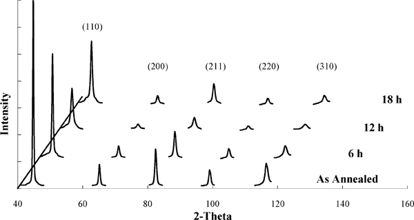
X-ray diffraction patterns of samples before and after milling treatments (Wi is integral breadth of Bragg reflection including instrumental broadening in 2θ scale)
Average grain size and mean microstrain of top surface layer after milling for different periods of time
In order to measure the case depth obtained under different experimental conditions, a metallographic technique was used. Metallographic images at magnification levels of ×50 and ×100 were taken from the samples carburised at 850 and 800°C respectively. The magnification level was chosen in such a manner so that the field of view was at least 1·5 times of the coating thickness.31,32 Automatic image processing was performed with the same threshold light intensity for a region of 900 μm length for each sample. The microstructure and image processing results of the samples carburised at 800°C for 15 min are shown in Fig. 4. The average depth of the carburised layer for the sample milled for 12 h was 84 μm (Fig. 4d), whereas the measured value for the unmilled sample was 47 μm (Fig. 4c). It could be seen that the carburised layer thickness of the sample milled for 12 h has been increased by ∼80 with respect to the unmilled one. The measured values of thickness for all the samples are presented in Table 2.
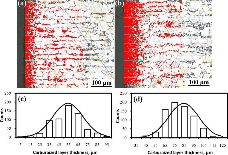
Surface microstructure and thickness distribution of carburised layer after carburising at 800°C for 15 min (solid lines are normal curves that were plotted to compare distribution of data)
Measured depths of carburised layer obtained by different methods
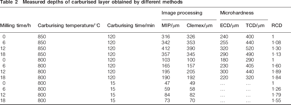
Figure 5 shows the hardness profiles for the samples carburised at 850 and 800°C for 120 min. The hardness values of the samples carburised at 800°C for 15 min had a remarkable error that was due to the small thickness of the carburisation layer. For this reason, the results are not reported here.
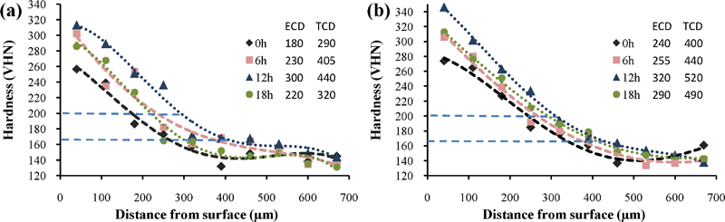
Hardness profiles of samples after carburising at a 800°C for 2 h and b 850°C for 2 h
The values of the total case depth (TCD) and effective case depth (ECD) were also estimated using the depicted curves (Fig. 5). The TCD represents the depth at which the hardness is 10 higher than that of the core.32,33 In this case, the ECD was determined as the distance from the surface at which the hardness value is >200 HV.
On the basis of the metallographic investigations and microhardness measurements presented in Table 2, it was found that, although the values of TCD and ECD differ from the reported values obtained by image processing, variations of these parameters possess a similar trend. The same differences were also reported previously in other studies. The value measured from the metallographic images is usually lower than that obtained from the microhardness measurements.26 It was also observed that the thickness values calculated by both image processing programmes are in good agreement with each other (the difference is <6).
In order to better compare the data summarised in Table 2, relative case depth (RCD) was defined for each carburising condition. This parameter is obtained by dividing the value of carburised layer thickness to the one for the unmilled sample. The data from MIP software were used to calculate the RCD. As can be seen, the highest efficiency was achieved for the sample which was milled for 12 h and then carburised at 800°C for 120 min. The carburised layer thickness in this sample is ∼90 greater than that of the unmilled sample.
It is also obvious that in all cases the samples which were ball milled for 12 h own the greatest carburised thickness value. This is consistent with the SEM and XRD results in which the highest amounts of cold work and grain refining were observed in the sample milled for 12 h.
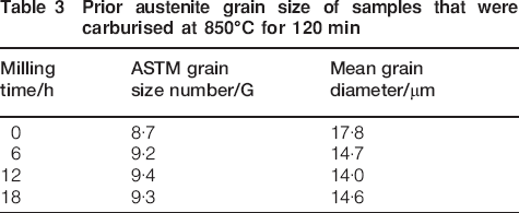
In order to investigate the effect of prior austenite grain size on the carburised depth, austenite grains were revealed in the samples which had been carburised at 850°C for 2 h. As can be seen from Fig. 6, the prior austenite grains are fairly distinguishable in the optical micrograph of the carburised samples. The average grain size of the samples was evaluated using the intercept method described in ASTM E-112. The results are listed in Table 3. It can be seen that the austenite grain size of the unmilled sample is greater than that of the milled samples. Figure 7 compares the values of the prior austenite grain size with the RCD for the samples which were carburised at 850°C for 120 min. As was expected, the variation in austenite grain size is in good agreement with the RCD. It is also apparent that the sample milled for 12 h, which possessed the greatest amounts of stored energy and structural defects, owns the lowest austenite grain size and the greatest carburised layer thickness.
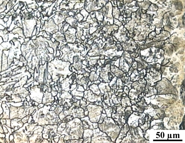
Prior austenite grain boundaries in surface layer of sample milled for 12 h and then carburised at 850°C for 2 h
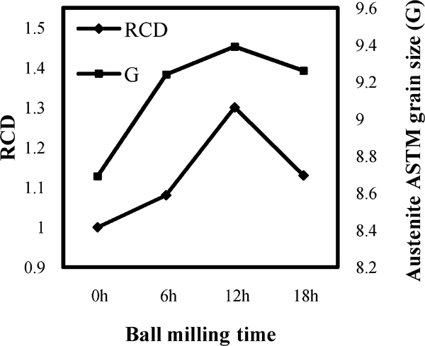
Comparison of RCD and austenite ASTM grain size as function of milling time
Prior austenite grain size of samples that were carburised at 850°C for 120 min
It can be concluded that the surface nanocrystalline structure obtained by BM has two effects on the subsequent carburising treatment. First, especially in the initial stages of treatment, a large number of grain boundaries with various kinds of non-equilibrium defects greatly accelerate the kinetics of the carburising treatment. Second, the high amount of stored energy in the surface layers reduces the transformed austenite grain size that would be effective on carbon diffusion enhancement in subsequent stages of carburising treatments.
Conclusions
In the present study, a nanograined surface layer was prepared in an Fe–0·15C steel by the BM method. The highest amounts of cold work and grain refining in the surface layer were achieved by milling for 12 h. The influence of this SPD on the following carburisation treatment was also studied. It was observed that the carburised layer thickness could be approximately doubled by applying surface milling as a pretreatment to the carburising stage. Once again, the best improvement in the carburising efficiency was observed in the samples milled for 12 h. The nanostructured surface layer with great amounts of imperfections and stored energy was known to be the primary reason for the observed increase in case depth during the carburising treatment.
Footnotes
Acknowledgements
The authors would like to acknowledge Nahamin Pardazan e Asia Co. for providing the MIP Microstructural Image Processing Software.