
Abstract
Hydrogen doped In2O3 (In2O3:H) films show high conductivity, small dispersion of refractive index and very low extinction coefficient in the visible to near infrared wavelengths. The improved properties make this transparent conducting oxide an ideal candidate for a window electrode of optoelectronic devices. This article describes the control of microstructure of In2O3:H, the relationship between the structure and transport properties and the Si based solar cells incorporating the In2O3:H window electrode.
Keywords
Introduction
Transparent conductive oxide (TCO) films are increasingly essential in rapidly growing optoelectronic applications, such as flat panel displays and solar cells. Continuous development of high performance optoelectronic devices stimulates the research on TCO films. So far, high conductivity and high transparency in the visible wavelengths are required for TCO films in display applications, and Sn doped indium oxide (ITO), indium zinc oxide (IZO) and Al doped zinc oxide have been developed. On the other hand, for TCO films in solar cell applications, high transparency up to the near infrared (NIR) wavelengths is also required in order to increase the conversion efficiency of solar cells by improving the spectral sensitivity in the visible to the NIR wavelengths.1 – 6 The high transparency in the NIR wavelengths can be achieved by the reduction of free carrier absorption, i.e., increase in mobility and decrease in carrier density, provided that the same conductivity is required.7 Recently, we have developed H doped indium oxide (In2O3:H) films with high electron mobility (⩾100 cm2 V−1 s−1) and low carrier density (⩽2×1020 cm−3) by solid phase crystallisation of amorphous In2O3:H films.8 The values of mobility are factors of 2–3 greater than those of conventional ITO9 – 11 and amorphous IZO, 12 12,13 and the process temperature is <200°C. Therefore, the films show enormous potential for window electrodes for heat sensitive devices and/or substrates.
The key issues to realise high electron mobility in the In2O3:H films are control of microstructure and stoichiometry of the films. This paper describes the control of the microstructure of In2O3:H and the relationship between the structure and transport properties. Furthermore, the study of the electrical and optical properties of the In2O3:H developed so far with the aim of improving the solar cell efficiency and the study of Si based solar cells incorporating the In2O3:H are reviewed and discussed.
Experimental
Approximately 70 nm thick In2O3:H thin films were grown on 50 nm thick SiO2 coated Si without any intentional substrate heating by a radio frequency magnetron sputtering method. To incorporate H into the In2O3 matrix, H2O vapour has been introduced into the chamber during sputtering of an In2O3 ceramic target.8 We introduced H2O vapour from a heated water vessel using a variable leak valve or a humidification system (RASIRC, RainMaker), which can provide controlled delivery of ultrapure water vapour into Ar gas. The base pressure of the chamber was <5×10⁻⁶ Pa. The total gas pressure of Ar, O2 and H2O during deposition was 0·5 Pa with an O2/(Ar+O2) ratio of 0·0038. The H2O partial pressure was monitored using quadrupole mass spectrometry. After the deposition, the films were post-annealed in vacuum at 200°C for 2 h.
Structural changes of the films were evaluated by X-ray diffraction (XRD), plan view transmission electron microscopy (TEM), electron diffraction, atomic force microscopy (AFM) and thermal desorption spectroscopy (TDS). The incident angle of X-ray was 0·8°. Thermal desorption spectroscopy was applied to investigate desorption gases from the films during the annealing process. Films on SiO2 coated Si were heated at a constant rate of ∼16°C min−1 by an infrared ramp. The temperature was calibrated using a thermocouple in direct contact with the film surface. The gases desorbed from the specimens were identified by quadrupole mass spectrometry. Thermal desorption spectroscopy was also used to estimate the H composition in the films from the TDS signals of H2O desorbing from the films during the heat treatment up to 750°C. The atomic concentration of H was obtained by normalising the TDS signals using H compositions for 240 nm thick films characterised by hydrogen forward scattering spectrometry and TDS.8 In this study, we measured the H composition for the as deposited films. The electrical resistivity, carrier density and mobility of the films were obtained in the van der Pauw configurations using Hall effect at room temperature. The thickness and optical constants of the In2O3:H films were measured using spectroscopic ellipsometry. Details of the measurements and data analysis procedures have been reported elsewhere.14
Results and discussion
Structural properties
Figure 1a and b shows XRD patterns of the as deposited and post-annealed In2O3:H films grown at different H2O partial pressures respectively. It should be noted that the as deposited In2O3:H film having H composition of 0·78 at-% was grown without intentional H2O introduction. In addition, we used larger receiving and scattering slits for the measurements of the as deposited In2O3:H (1·9 and 3·2 at-%H) films as compared with the other films. As shown in Fig. 1a, the structure changes from polycrystalline to amorphous phases with increasing H2O partial pressure during growth. The results indicate that the adhesion of H atom, OH or H2O molecules at growing surfaces suppresses the growth of crystallites. After post-annealing, the amorphous phase changes to a polycrystalline one with narrow diffraction peaks and random orientation, as shown in Fig. 1b. From previous XRD studies for 240 nm thick films,15 the solid phase crystallised In2O3:H films were free from strains, while the vapour phase crystallised films had strained lattices. Figure 2 shows the plan view TEM images for the as deposited In2O3:H (0·78 at-%H) (Fig. 2a) and as deposited (Fig. 2b) and post-annealed (Fig. 2c) In2O3:H (3·2 at-%H) films. In Fig. 2a, the In2O3:H (0·78 at-%H) film shows a grain structure. The grain size is about 20–30 nm, and the grains are shown to be defective. Nanobeam electron diffraction patterns gave multiple crystal patterns, indicating that multigrains exist along the growth direction. After the post-annealing process, no large structural change was observed (not shown). On the other hand, the as deposited In2O3:H (3·2 at-%H) film is mostly amorphous and includes some numbers of crystalline grains in it, as shown in Fig. 2b. The averaged size of the grains was ∼66 nm, and many of the nanobeam electron diffraction patterns of grains gave a singly crystal pattern. After the post-annealing process, the amorphous phase disappears, and the film shows a grain structure with very large grains, as shown in Fig. 2c. The average size of the grains was ∼440 nm. These results clearly show that solid phase crystallisation of amorphous In2O3:H is quite effective to obtain larger grains with higher crystallinity compared with the vapour phase crystal growth.
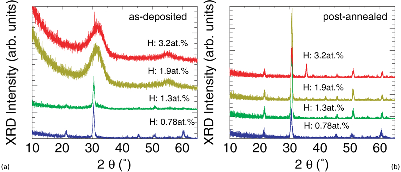
X-ray diffraction 2θ scan profiles of a as deposited and b post-annealed In2O3:H films grown at different H2O partial pressures
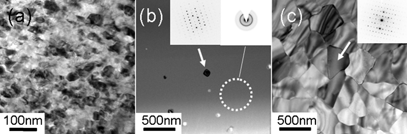
Plan view TEM images for a as deposited In2O3:H (0·78 at-%H) and b as deposited and c post-annealed In2O3:H (H, 3·2 at-%) films: in b and c, nanobeam electron diffraction patterns of grains depicted by arrows and selected area electron diffraction pattern of dotted region are also shown
The structural change with increasing H2O vapour pressure is also observed in the surface morphology. Figure 3a–d and e–h shows the AFM images of 2×2 μm regions of the as deposited and post-annealed films having H compositions of 0·78, 1·3, 1·9 and 3·2 at-% respectively. The values of root mean square roughness in Fig. 3a–h are 0·91, 0·31, 0·17, 0·20, 0·78, 0·33, 0·21 and 0·22 nm respectively. With increasing H2O vapour pressure, the surface roughness of the as deposited films decreases due to the suppression of crystallite growth. Furthermore, solid phase crystallisation of the amorphous In2O3:H films maintains the smooth roughness.
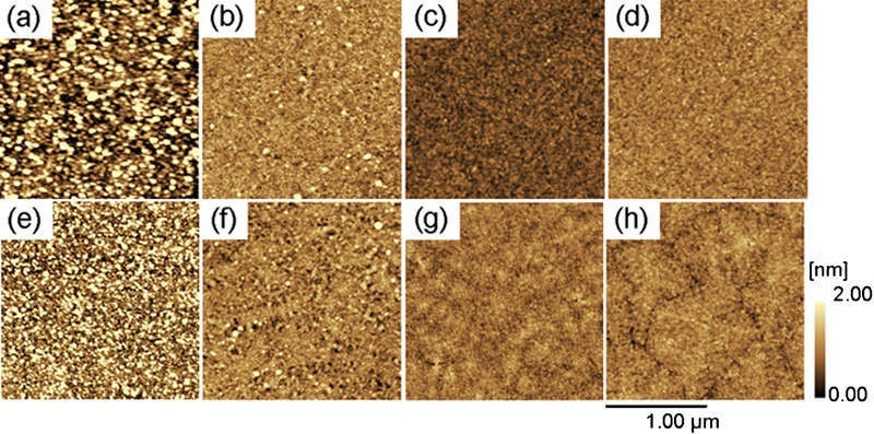
Images (AFM) of as deposited and post-annealed In2O3:H films having H composition of a, e 0·78 at-%, b, f 1·3 at-%, c, g 1·9 at-% and d, h 3·2 at-%
The behaviours of desorption species from the films during the annealing process are also different with H composition in the films. Figure 4 shows the TDS spectra of desorption species from the films. We monitored signals of H2 (m/z = 2, where m/z indicates the molecular mass/charge ratio), H2O (m/z = 18), O2 (m/z = 32), In (m/z = 115) and InOH (m/z = 132). The signal of In2O (m/z = 246) that is also volatile could not be measured due to the limitation of the maximum mass number of the quadrupole mass spectrometry used in this study. The films show complex variations in the TDS signals, which can be categorised into four temperature regions, especially for the In2O3:H films grown under intentional H2O introduction: T⩽210°C (region I), 210°C⩽T⩽380°C (region II), 380°C⩽T⩽570°C (region III) and 570°C⩽T⩽700°C (region IV). Similar variations in TDS signals were also observed for the as deposited In2O3:H (3·2 at-%H) and post-annealed films.16 From comparative studies using TEM and TDS for the as deposited and post-annealed films at various temperatures, these desorption states are considered to be closely related to the microstructure of the films. In the region (I), the first and second peaks of the H2O signal are attributed to the physically adsorbed and hydrogen bonded water molecules that exist inside the films, for example, at surface of micro- or macropores in amorphous phase. In particular, the second peak occurs with crystallisation of the film. In region II, the broad desorption characteristics of H2O and H2 signals suggest a necessary prediffusion of internal H2O related species to the grain boundary and/or surface before desorption; during heating, H or OH inside grains segregate at grain surfaces and react with a neighbouring H at the surfaces and finally generate H2 and H2O molecules. In region III, the rapid increase in the H2O and In related species implies a fast decomposition of indium hydroxide formed on the grain surfaces. In region IV, oxygen desorbs just after finishing desorption of H2, H2O and In related species due to the voids at the grain boundaries and the substructures inside grains that are formed during heating in region III.
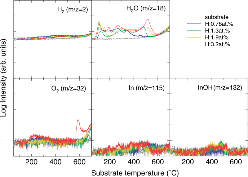
Spectra (TDS) of as deposited In2O3:H films having different H compositions for H2 (m/z = 2), H2O (18), O2 (32), In (115) and InO (132)
In Fig. 4, the desorption behaviour of the In2O3:H (0·78 at-%H) film grown without intentional H2O introduction is completely different with that of the other films. With increasing H2O partial pressure, the temperature of the second peak of the H2O signal in region I increases. This result indicates that the crystallisation temperature increases with H. The change in crystallisation temperature is considered to be due to the decrease in the density and/or size of crystalline nuclei with the increase in H composition, since crystallisation proceeds from small crystalline nuclei observed in the as deposited films.16 Furthermore, the total amount of H2O desorption in regions II and III increases with H composition, indicating the increase in chemically bonded H in the films.
Electrical properties
Figure 5 shows the resistivity, carrier density and mobility of the films as a function of H composition in the films. The transport properties show a direct relationship with the structure shown in Fig. 1 and are categorised into three groups, i.e. group I, polycrystalline films grown by vapour phase crystal growth; group II, amorphous films; and group III, polycrystalline films grown by solid phase crystallisation. The as deposited films (<1·3 at-%H) in group I show high resistivity (>10−2 Ω cm) with low carrier density (1–2×1019 cm−3) and mobility (⩽20 cm2 V−1 s−1). No large change is observed after the post-annealing process. On the other hand, the as deposited films (>1·3 at-%H) in group II show lower resistivity (3–4×10⁻⁴ Ω cm) with larger carrier density (∼5×1020 cm−3) and mobility (∼40 cm2 V−1 s−1). The post-annealed films (⩾3·2 at-%H) in group III show further large mobility (∼110 cm2 V−1 s−1) with small decrease in carrier density (∼2×1020 cm−3).
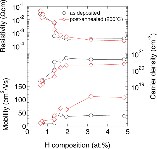
Resistivity, carrier density and mobility of as deposited and post-annealed In2O3:H films as function of H composition
The carrier density and mobility of the as deposited films, determined by Hall measurements, increase with H composition. This is considered to be due to the reduction of grain boundaries and microscopic defects inside the crystalline grains. These defects can capture electrons, acting as acceptor-like centres. Potential barriers created by the accumulation of acceptor-like centres in the grain boundaries and space charges formed around the defects in the crystalline grains scatter electrons travelling across them. Therefore, the carrier density and mobility increase with decreasing volume fraction of the crystalline phase that is composed of defective grains. In addition, H is considered to passivate the acceptor-like centres with the form of OH.
On the other hand, a large increase in mobility and a decrease in carrier density are observed after solid phase crystallisation. The increase in mobility was confirmed to be attributed mainly to the longer relaxation time rather than the smaller effective mass from previous spectroscopic ellipsometry analyses.16 Temperature dependent Hall analysis, relationship between carrier density and mobility and comparison among Hall mobility, optical mobility and calculated mobility dominated by ionised impurity scattering suggest that H doping reduces carrier scattering in the crystallised In2O3, and structural rearrangements during crystallisation eliminate oxygen deficiency and generate H+ that acts as a singly charged donor.16
Optical properties
Figure 6 shows the refractive index and extinction coefficient of the In2O3:H (∼3 at-%H) films post-annealed at 200°C. For comparison, optical constants of an ITO (90 wt-%In2O3 and 10 wt-%SnO2) film that was also fabricated by the similar process17 and exhibited similar resistivity are also shown in Fig. 6. The electrical properties of the films are as follows: resistivity of 3·07×10−4 Ω cm, carrier density of 1·61×1020 cm−3 and mobility of 126 cm2 V−1 s−1 for In2O3:H and resistivity of 2·08×10−4 Ω cm, carrier density of 1·25×1021 cm−3 and mobility of 24·0 cm2 V–1 s–1 for ITO. In Fig. 6, both TCO films show an increase in extinction coefficient and a decrease in refractive index at longer wavelengths due to the effects of free carrier absorption. However, the changes are quite small in the In2O3:H film as compared to the ITO film since the influences of free carrier absorption in the In2O3:H film are well suppressed by high mobility and low carrier density.
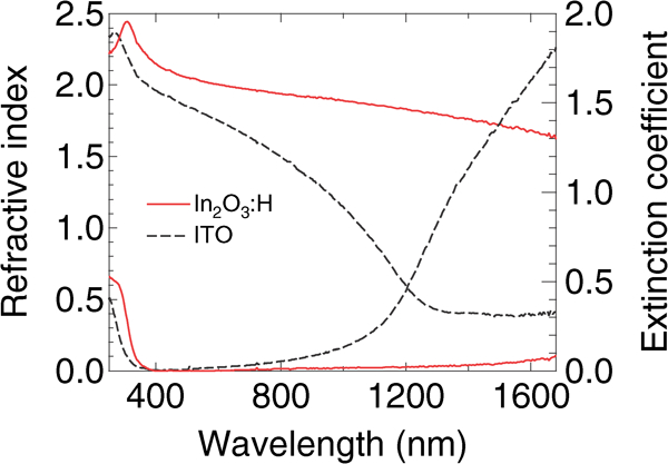
Refractive index and extinction coefficient of In2O3:H and ITO films post-annealed at 200°C
Applications for optoelectronic devices
The In2O3:H TCO films show a small dispersion of refractive index and a very low extinction coefficient in the visible to NIR wavelengths, as shown in Fig. 6. Therefore, one can design high performance coatings, for example, antireflection coating and low absorption loss coating, in optoelectronic devices, including solar cells and photo detectors. For example, ITO is usually used as a window electrode with an antireflection effect in a-Si:H/c-Si heterojunction solar cells and thin film substrate type solar cells. With an improvement in the quality of the absorbing layers and light trapping techniques of the solar cells, optical losses originating from the window electrode become important factors for obtaining higher efficiency. We have fabricated two types of Si based solar cells incorporating the In2O3:H, i.e. a-Si:H/c-Si heterojunction solar cell17 and thin film microcrystalline Si solar cell.18 The structures of the heterojunction and thin film solar cells were Ag grid/In2O3:H (72 nm thick)/a-Si:H p layer/a-Si:H i layer/n-type c-Si (525 μm thick)/Al and Ag grid/In2O3:H (72 nm thick)/μc-Si:H p-i-n layers (i layer, 2 μm thick)/ZnO:Ga/Ag/textured substrate respectively. Both solar cells incorporating the In2O3:H layer showed higher current density and the resulting conversion efficiency as compared with the solar cells incorporating the ITO films. Optical analysis of the solar cells, TCO films and Si layers revealed that the improvement in current density for the a-Si:H/c-Si heterojunction solar cell is due to the reduction of reflection loss at the front TCO/a-Si:H interface and the absorption loss caused by free carriers within the TCO layer in the visible to NIR wavelengths, while for thin film microcrystalline Si solar cell, it is due mainly to the reduction of the absorption loss.
Conclusion
The microstructure of In2O3:H films fabricated at room temperature by radio frequency magnetron sputtering can be controlled by changing the partial pressure of H2O during sputtering and the post-annealing process. Their electrical properties are strongly dependent on the microstructure: low mobility (⩽20 cm2 V−1 s−1) and low carrier density (1–2×1019 cm−3) for vapour phase crystallised films with small defective grains (20–30 nm), high mobility (∼40 cm2 V−1 s−1) and high carrier density (∼5×1020 cm−3) for amorphous films and very high mobility (∼110 cm2 V−1 s−1) and relatively low carrier density (∼2×1020 cm−3) for solid phase crystallised films with high crystallinity and large grains (∼440 nm). The change in carrier density and mobility is explained in the view point of structural defects that act as acceptor-like centres, passivation of the acceptor-like centres by H and change in the carrier generation mechanism by solid phase crystallisation. The solid phase crystallised In2O3:H films show low resistivity, small dispersion of refractive index and very low extinction coefficient in the visible to NIR wavelengths due to high mobility and low carrier density. The films show enormous potential for window electrodes for optoelectronic devises. The feasibility of the films has been demonstrated for a-Si:H/c-Si heterojunction solar cells and thin film microcrystalline Si solar cells and confirmed the improvement of spectral sensitivity and resulting conversion efficiency of the solar cells due to the reduction of reflection loss at the front TCO and absorption loss within the TCO in the visible to NIR wavelengths.
Footnotes
Acknowledgements
The authors would like to thank RASIRC founder J. Spiegelman, Mr K. Sugihara, Mr N. Tomita and Mr M. Tada of Taiyo Nippon Sanso Corporation for their technical advice on the controlled delivery of water vapour in the growth chamber using the humidification system. This work was supported by the New Energy and Industrial Technology Development Organization (NEDO) under the Ministry of Economy, Trade and Industry (METI), Japan.