
Abstract
ZnMgO thin films deposited on Si (111) substrates by pulsed laser deposition at 300°C were annealed at different temperatures from 400 to 800°C in air. Non-polar films with (110) orientation have been obtained. The thin film annealed at 500°C shows the co-existence of (002), (200) and (110) orientations according to X-ray diffraction observation, which illustrated that Mg has been incorporated into ZnO. Scanning electron microscopy images and energy dispersive X-ray revealed the variation of surface morphology and element content. The largest band gap value has been determined to be 4·31 eV when the film was annealed at 700°C. The typical peaks of Zn–O and Mg–O bonds were observed in the IR spectrum. The shift of UV peaks in photoluminescence spectra emerged due to the increase in Mg doping as the annealing temperature increases.
Introduction
ZnMgO alloys have been attracting considerable attention for optoelectronic devices based on ZnO, in particular, for UV region light emitting diodes.1, 2
Magnesium oxide (MgO) is an ideal material for widening the band gap of ZnO. Ternary ZnMgO alloy is recognised as a suitable barrier layer material based on the ZnO heterostructure for controlling the carrier concentration. The radii of Zn2+ and Mg2+ are 0·57 and 0·60 Å,3 respectively. Similar radii avoid the formation of high intensity defects resulting from the stress mismatch when alloying. Furthermore, the band gap energy of ZnMgO can be tuned in a large range from 3·37 to 7·8 eV according to the different concentrations of the Mg element.4 Since Ohtomo et al.5 successfully prepared ZnMgO thin films on sapphire substrates by pulsed laser deposition (PLD) technique, other techniques have been employed to prepare ZnMgO films as well, such as magnetron sputtering, molecular beam epitaxy, metalorganic chemical vapour deposition, sol–gel, etc. There have been lots of reports about the preparation of c axis Zn1−xMgxO thin films by varying Mg contents, fabricated temperature, etc.6, 7 However, the degraded effects on the electronic and optical properties of ZnMgO thin films are raised owing to a quantum confined Stark effect due to the large internal electric fields along the c axis of ZnMgO (polar axis).8 Therefore, the non-polar growth of ZnMgO thin films by employing various technologies is important for preventing this effect.9, 10 However, few studies have shown that the annealing can change the band gap of ZnMgO thin films, and non-polar ZnMgO thin films have be obtained by post-annealing as yet. In this paper, we have obtained the ZnMgO thin films along the (110) zone axis by post-annealing, and the effect of annealing temperature on the composition, structure, band gap and optical properties of ZnMgO thin films was investigated.
Experimental
ZnMgO thin films were deposited on Si (111) substrates by PLD technique at growth temperature of 300°C. The details of our experimental set-up were described in Ref. 11. That is, a KrF excimer laser (the wavelength is 248 nm, the repetition is 10 Hz and the duration is 25 ns) was used to ablate the target (with the 10 at-%Mg content by mixing ZnO and MgO powders), and the laser incident energy was kept as 200 mJ/pulse. The deposition time was 15 min. Then, ZnMgO thin films were annealed immediately at different temperatures from 400 to 800°C for 10 min in air ambience in a tubular furnace (model OTF1200X-II). Crystal structure orientation was determined by X-ray diffraction (XRD; λ = 0·1541 nm, D8-advance), surface morphology was observed using field emission scanning electron microscopy (QUANTA 250) and energy dispersive X-ray (EDX) spectroscopy was employed to measure the element contents and the EDX spectra of the annealed ZnMgO thin films. A France SOPRA GES-5 type spectroscopic ellipsometer was used to measure the optical parameters and the thicknesses of ZnMgO thin films. The IR spectra were carried out by employing a BRUKER TENSOR27 spectrophotometer in transmission mode. The photoluminescence (PL) spectra were investigated by employing a PerkinElmer LS55 fluorescence spectrometer with the excitation wavelength of 325 nm pumped by a high energy pulsed Xe source.
Results and discussion
XRD analysis
Figure 1a–e shows the XRD spectra of ZnMgO films annealed at various temperatures from 400 to 800°C. The film annealed at 400°C presents a weak (002) peak corresponding to a c axis ZnMgO hexagonal structure. The (002) and (200) peaks correspond to the ZnMgO cubic structure, and a non-polar (110) orientation is presented for the film annealed at 500°C, indicating that the Mg atom is substituting the Zn atom in the ZnMgO thin film by annealing. One reason is that it is easier for the Mg atom to lose electrons than the Zn atom due to the different Pauling electronegativities (Mg is 1·31, and Zn is 1·65) as the Mg and Zn atoms bond with O atom, resulting in the increase in the quantity of Mg–O bond. Interestingly, with the increase in the annealed temperature, the non-polar (110) orientation of ZnMgO thin films is obtained. The full width at half maximum (FWHM) of the XRD (110) peak is decreasing, as shown in Table 1, indicating the crystal quality of ZnMgO thin films is getting better. Meanwhile, it should be noticed that the intensity of the (110) peak was reduced when the annealing temperature was >600°C. Generally, the FWHM of the XRD depends on the crystalline quality of each grain and the distribution of grain orientation. The increase in the FWHM and the decrease in intensity of the XRD for ZnMgO thin films annealed at temperature above 600°C can explain that the crystalline quality of each grain and grain orientation becomes poor. The annealing temperature of 600°C is the optimum.
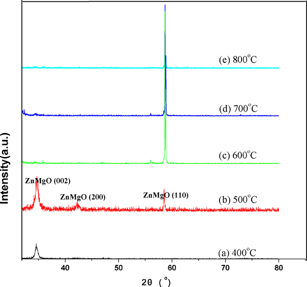
X-ray diffraction spectra of ZnMgO films annealed from 400 to 800°C
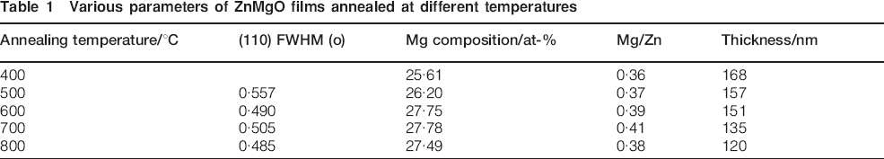
Various parameters of ZnMgO films annealed at different temperatures
It can be noticed that the ZnMgO (002) diffraction peak shifts from 34·56 to 34·70° for ZnMgO thin films annealed from 400 to 500°C. This can be caused by the increase in substituted Mg2+ in ZnMgO crystal with the increasing annealed temperature. The radius of Mg2+ (0·57 Å) is smaller than that of Zn2+ (0·60 Å). Therefore, the lattice constant d is decreasing with the increasing incorporation of Mg contents in ZnMgO thin films. According to the Bragg equation (that is 2dsin θ = nλ), the diffraction angle 2θ is increased. An obvious ZnMgO (200) peak located at 42·34° can be observed for the ZnMgO film annealed at 500°C. The (200) peak has a slight deviation towards the low angle compared with the 2θ value of MgO (200) diffraction peak (42·98°), which is also an indication that the Mg content doped into the ZnMgO films is increased by post-annealing. The increase in Mg content with the increasing annealed temperature is further proved by EDX measurement, as shown in Table 1.
SEM observation
Figure 2a–f shows the SEM images of the ZnMgO thin films as grown and annealed from 400 to 800°C respectively, and Fig. 2g shows the EDX spectrum of the ZnMgO thin film annealed at 600°C. The quality of the thin films is improved with increasing annealed temperature, as observed in Fig. 2a–d. The average grain size increases, and the distribution of grain orientation is more aligned. The even grains and smooth and compact surface can be obtained for the ZnMgO thin film annealed at a temperature of 600°C. As the annealing temperature is >600°C, some large grains emerge on the ZnMgO thin films due to the redistributed crystalline grain by supplying sufficient thermal energy, and the small grain island has been joined into the great crystalline surface. Considering the observation of XRD, it is proposed that the preferential (002) orientation growth of the ZnMgO thin films annealed at high temperature is suppressed by the redistributed crystalline grain, and non-polar (110) zone axis growth is formed. Figure 2f shows the EDX spectrum of the ZnMgO film derived from Fig. 2d, and the C, O, Zn, Mg, and Si peaks can be observed, indicating the ZnMgO film with proper contents was formed by annealing.
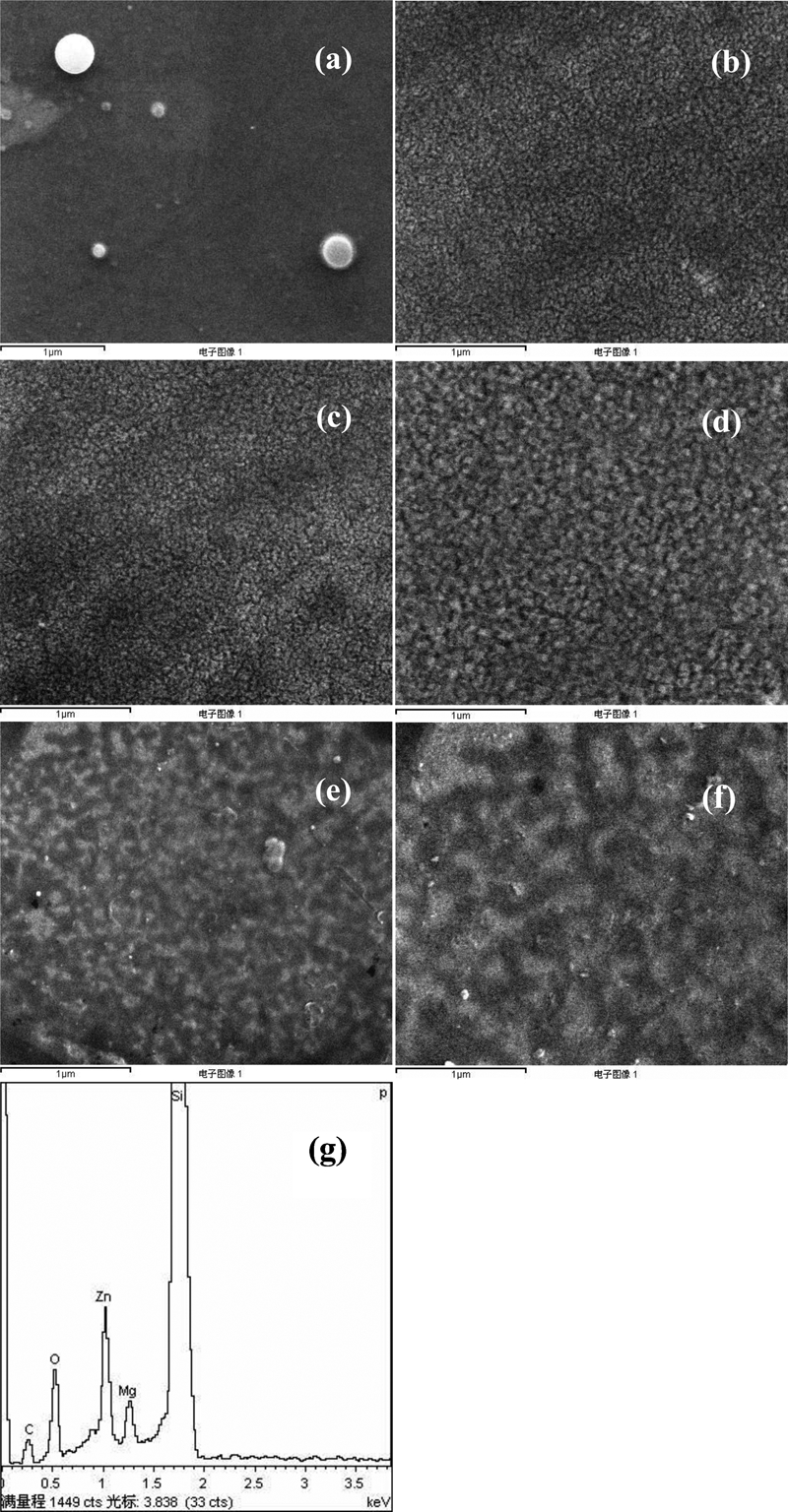
Images (SEM) of ZnMgO samples
The atomic concentration of the Mg element increases in the range of 25·61–27·78% for the ZnMgO film annealed from 400 to 800°C, as shown in Table 1. The ratio of the Mg/Zn of the ZnMgO films is also given in Table 1. Therefore, the film can be considered as Zn0·73Mg0·27O due to the small changes of Mg content. The thickness values of the annealed ZnMgO films are decreasing gradually, as shown in Table 1. One reason is the surface element evaporation of the ZnMgO thin films owing to the thermal fluctuation energy of some adatoms overcoming the attachment energy as the annealing temperature increases. The other reason is the surface contraction of the ZnMgO thin films owing to the elimination of vacancies and defects formed at the deposition process or resulting from increasing grains with the annealed temperature from 400 to 800°C.
Band gap measurement
Figure 3 shows the variation of (αhν)2 versus hv for ZnMgO films with the variation of the annealing temperature. The optical band gaps can be obtained from the transmission spectra by Tauc's method,12 that is, plotting (αhν)2 versus hv, and extrapolating the straight line portion of this plot to the energy axis, where α is the absorption coefficient, and hv is the photon energy, i.e.

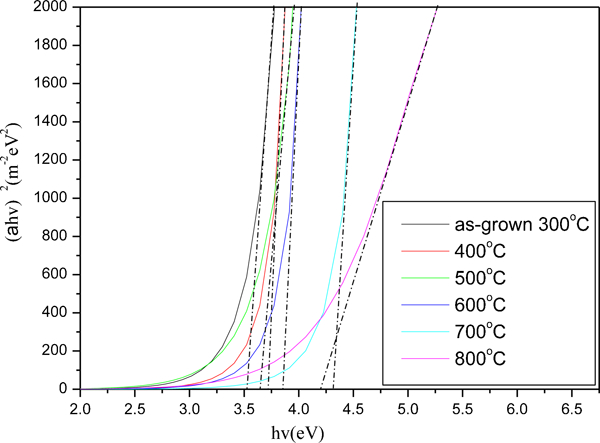
(αhν)2 versus photon energy (hv) of ZnMgO films as grown at 300°C and annealed from 400 to 800°C
The variation of band gap energy is related to the Mg concentration variation, which has been confirmed by Ohtomo et al.5 The band gap of the ZnMgO thin films can be adjusted by post-annealing.13 The Mg element is more active than that of Zn, and the standard Gibbs free formation energy of MgO (−375·72 kJ mol−1) is less than that of ZnO (−569·55 kJ mol−1). It is possible that the separation of Mg or O band was formed easily in ZnMgO crystal lattice owing to the rapid and unequilibrium growth during the PLD deposition procedure. The Mg can acquire enough energy into the ZnO crystal lattice and instead of Zn as the ZnMgO thin films were annealed at increasing temperature, resulting in the increase in ZnMgO band gap.
IR absorption spectrum
Figure 4 shows the recorded IR spectrum of the ZnMgO thin films as grown at 300°C and annealed at 600°C in the range from 400 to 1300 cm−1. As shown in Fig. 4, the peak located at 421 cm−1 is the typical ZnO absorption due to the bending vibration absorption of the Zn–O bond. The typical peak of the Mg–O bond is observed at the absorption band from 513 to 565 cm−1. The broad peak observed at 609 cm−1 is the local vibration of the substitutional carbon in the Si crystal lattice.14 The peak located at 873 cm−1 (a stretching vibration absorption of Si–C bond of crystalline SiC) and 1108 cm−1 (a vibration absorption of Si–O bond) may be caused during the cooling process and the thermal annealing in air.15 It should be noticed that the absorption peaks located at 421 cm−1 and from 513 to 565 cm−1 become stronger for the ZnMgO thin film annealed at 600°C than that of the as grown thin film. This indicates that the quality of the ZnMgO thin films is improved and the Mg content doped into the films is increased by post-annealing.
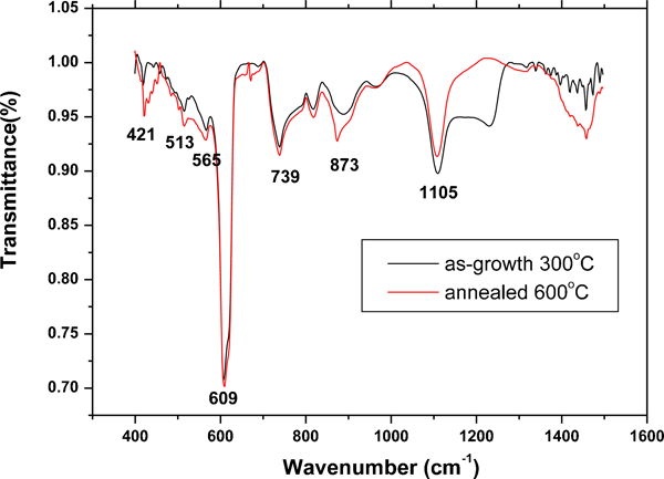
Infrared absorption spectra of ZnMgO thin films as grown at 300°C and annealed at 600°C
PL spectra analysis
Figure 5a–f shows the PL spectra of the ZnMgO thin films as grown and annealed from 400 to 800°C. As marked in Fig. 5, the dominant emission peaks are obtained using Lorentz fitting in the UV region, and three relative weak emission peaks in the visible region are observed. The peak located at ∼380 nm is ascribed to exciton recombination.16 The purple emission peak located at 421 nm (the energy level is 2·90 eV) should be the electronic transition between the donor level of the Zn interstitial (Zni) and the valence band.17 The blue emission peak located at 483 nm (the energy level 2·57 eV) is generally accepted as the defect emission of the oxygen vacancies or derived from the electronic transition between the donor level of Zni to the acceptor level of VZn (the energy level is 2·6 eV).18 The peak located at 530 nm (the energy level is 2·35 eV) can be considered as the electronic transition between the bottom of the conduction band level and the acceptor level of OZn considering the acceptor level of antioxygen (2·38 eV, OZn). The obvious change of the defect emission cannot be raised by post-annealing, but the increases in UV emission and Mg content are obtained as shown in the PL and EDX spectra.
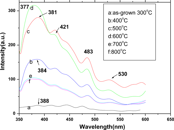
Photoluminescence spectra of ZnMgO films as grown at 300°C and annealed at temperature from 400 to 800°C
As shown in the PL spectra, the UV peaks are blue shifted from 388 to 377 nm with the increase in annealing temperature. The blue shift of the UV emissions is attributed to the increase in Mg contents, as proved in Table 1. The variation of the UV emission intensity is consistent with the XRD observation. It is concluded from the observation of the PL spectra that the best luminescence behaviour is obtained for the film annealed at 600°C. The wider band gap of the ZnMgO thin film by changing the annealing conditions creates an opportunity for the fabrication of optoelectronic devices.
Conclusions
The annealing effects on the structure, band gap and optical property of ZnMgO thin films have been investigated. The results have shown that the non-polar ZnMgO thin films were obtained owing to recrystallisation with the increasing annealing temperature. The coexistence of (002), (200) and (110) orientations was presented at the annealing temperature of 500°C due to the increasing Mg substitution. The film annealed at 700°C had the largest band gap energy of 4·31 eV. The emission mechanism of purple peaks at 421 nm, blue peaks at 483 nm and green peaks at 530 nm was derived from Zn interstitial, oxygen vacancies and antioxygen respectively. It is favourable to possess good structural and optical properties of ZnMgO thin films at annealing temperature of 600°C. The study provides an opportunity for constructing deep UV emission light emitting diode devices on the basis of the investigation of wide band gap ZnMgO thin films.
Footnotes
Acknowledgements
The authors are grateful for the financial support of the Shandong Provincial Natural Science Foundation (grant nos. Y2008A21, ZR2009FZ006 and ZR2010EL017), the Doctor Foundation of University of Jinan (grant no. XBS0833) and the Shandong Provincial Science and Technology Project (grant no. 2009GG20003028).