
Abstract
Copper aluminium oxide thin films were synthesised using the spray pyrolysis technique for different solvent volumes with a constant Cu/Al molar ratio. The preferential orientation is found along (100) and (102) planes, and the crystallite sizes are in the range from 21·6 to 28·4 nm. The structural studies reveal that the grown films were polycrystalline in nature. Hall effect results confirm that the grown films are p type. When the solvent volume is increased from 10 to 40 mL, the resistivity of the films decreases from 1·12 × 10− 6 to 6·2 × 10− 8 Ω cm. The band gap of the films increases with increasing the solvent volume. The obtained results show that the grown films can be used as the active layer in a solar cell.
Keywords
Introduction
In recent days, scientific communities concentrate much to tailor the properties of copper oxides. 1 The oxidation of copper is comparatively easier and finds its potential application in solar cells, catalysts, optoelectronics and chemical sensors. Kawazoe et al. reported that chemical modulation of the valence band throws the light on p type conductivity of copper aluminium oxide CuAlO2 (CAO). 2 In addition, the high transparency in the visible region and other properties of CuXO2 (X = In, Cr, Ga) shows that they are suitable for application in solar cells. 3 Compared to Cu2O, ternary compounds of CuXO2 exhibit more advantage. The direct optical band gap of CuAlO2 films is reported as 3·75 eV. 4 The high surface/volume ratio of nanostructured CuAlO2 can be used to tailor the electrical, optical and chemical properties, which depend on the size and morphology of CuAlO2.5,6 CuAlO2 is a compound where its delafossite structure is a p type transparent conducting oxide with high conductivity and transparency. 7 Delafossite compounds (ABO2) have direct applications in solar cells or touch panels, 8 luminescence properties, 9 ozone sensing property, 10 field emission 11 and applications in catalysis. 12 The CAO thin films can be prepared by several methods such as plasma enhanced chemical vapour deposition, 13 sputtering, 14 dip coating 15 and spray pyrolysis.4,16 The influence of solvent volume on CAO film results in improved electronic and optical properties.16,17
Literature reports are already available on CAO thin films, and the properties that are influenced by equal Cu and Al concentration or high Al concentration on CAO are discussed. However, in this work, the CAO films with high concentration of Cu are studied, which may be suitable for solar cell active layers.
Experimental
Preparation of thin film
The CAO thin films are synthesised by dissolving (CuCl2.2H2O) and (AlCl3) in doubly deionised water with [Cu]/[Al] molar ratio of 10:1. Four different volumes (10, 20, 30 and 40 mL) of precursor solutions are prepared, and they are sprayed onto the ultrasonically cleaned glass substrates that are kept at a temperature of 400°C. A fully automated spray pyrolysis system ((HOLMARC, HO-TH-01, India) is used for synthesis of CAO films. Table 1 describes the control parameter used in the present study during the synthesis of CAO films.
Control parameter
Characterisation
The thickness of the films is measured using a profilometer (Mitutoyo, SJ 301, USA), and the thickness is found to be ∼760 nm. The structural studies are carried out using X'Pert Pro MPD X-ray diffractometer with Cu Kα (λ = 0·15406 nm) radiation. The Hall effect studies are carried out using Ecopia HMS-3000 measurement system, which is used to measure resistivity, mobility, conductivity, Hall coefficient and charge carrier concentration of CAO films. The optical band gap and transparency are investigated using UV–Vis spectrophotometer (UV-3150). The surface morphology and elemental identification were obtained using field emission scanning electron microscopy (JEOL-6701F, Japan).
Results and discussion
Structural properties
The structural studies of the CAO are investigated using X-ray diffraction (XRD) measurement, which is used to identify the crystal structure and existing phases of CAO thin films. Figure 1 represents XRD patterns of samples for different solvent volume ratios, deposited at 400°C. All the prepared CAO films exhibit polycrystallinity, which is inferred with different plane orientations from the XRD spectrum.
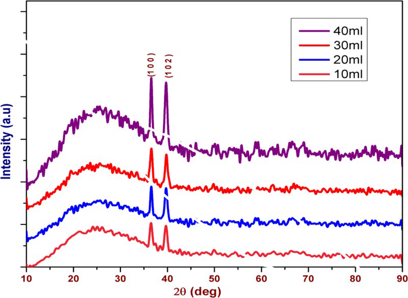
XRD patterns of CAO film for different thickness
The peaks in the XRD exactly match with International Centre for Diffraction Data card (JCPDS card no. 77-2494). Two prominent peaks are observed in the XRD pattern, which corresponds to (1 0 0) and (1 0 2) planes. This clearly confirms that the prepared films are the ternary compound of the CAO and the other phases are not present in the film. The mean crystallite size is calculated from well known Scherrer's equation,
18
which is given as

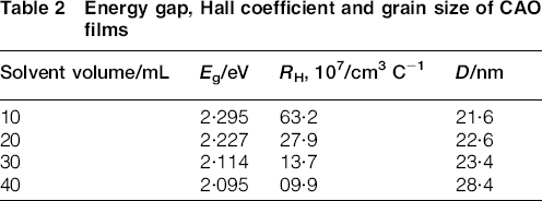
Energy gap, Hall coefficient and grain size of CAO films
Morphological properties
Figure 2 illustrates scanning electron micrograph (SEM) image of the CAO thin films deposited on glass substrates at 400°C for disparate solvent volume. From the SEM image, the morphology of the film shows uniformly distributed nanocrystallites. It is also observed that in CAO film, a highly oriented crystallites are formed for different solvent volume ratios. Moreover, the texture of the film is observed to be rough, which results in multiple reflection of light to take place on the surface of the film. This is one of the important characteristics of the film, which improves the p type active layer of solar cells. It is also observed that when the solvent volume increases, the size of polycrystalline grains increases. It can be concluded that CAO films are effective light scatters, which is one of the favourable properties to improve the efficiency of solar cell. 19 However, the rough surface of CAO is feasible for light trapping effect on amorphous silicon based solar cell, which was reported by Hu and Gordon.20,21
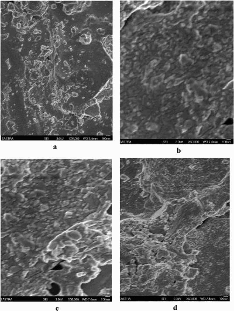
Surface morphology SEM images of solvent volume: a 10 mL, b 20 mL, c 30 mL and d 40 mL of CAO films
Optical Properties
Figure 3 shows the transmittance of spray deposited CAO films. The film shows a high transmittance in the near IR range, which shows that all the visible wavelengths are absorbed and it can be used for active layer in a solar cell.
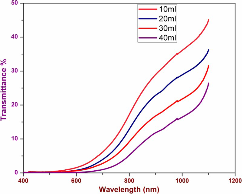
Optical transmittance spectrum of CAO thin films
The high transmission of ∼45% is observed in the IR region for a solvent volume of 10 mL. From Fig. 3, it is observed that the transmission of such film is strongly affected by the solvent volume of the films. The optical band gap Eg of CAO films is obtained by the absorption coefficient α and the incident photon energy hν, which is the relation of
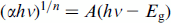
Graph between (αhν)1/2 versus hν for a 10 mL, b 20 mL, c 30 mL and d 40 mL solvent volume
Electrical properties
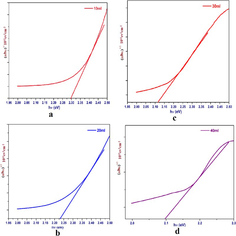
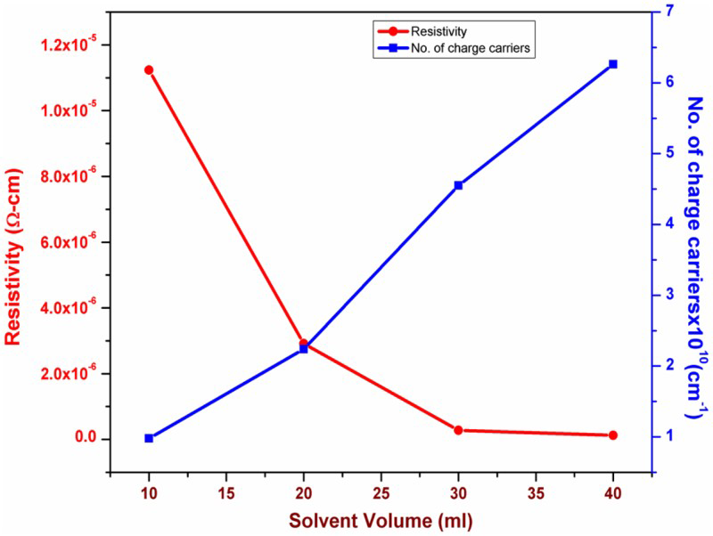
The Hall effect studies of CAO thin film with different solvent volume shows p type behaviour, and Hall coefficient (RH) decreases with increasing the solvent volume. The mobility, resistivity and carrier concentration are plotted in Fig. 5 as a role of CAO solvent volume. From Fig. 5, it is observed that the resistivity drops from 1·12 × 10− 6 to 6·2 × 10− 8 Ω cm for the solvent volume from 10 to 40 mL. In addition, the carrier concentration is found to be >0·98 × 1010/cm3 and increases with solvent volume. The decrease in resistivity for the CAO films from 10 to 40 mL volumes may be attributed to the increase in hole concentration originating from the increase in volume of precursor solution. Moreover, the charge carrier density substantially increases with increase in volume of precursor solution. From Table 2, it was observed that the grain size increases with the increment of solvent volume due to grain boundary scattering effect. 17
Plot between sample thickness versus resistivity and charge carrier concentrations
The cation vacancies (such as Cu vacancies) or oxygen interstitials are supposed to induce holes within the materials that can enhance conductivity. 23 The grain size dependence of carrier mobility is expressed from Fig. 6. The carrier mobility amends linearly with solvent volume, which is consistent with the enhancement preferred growth.
Plot between sample thickness versus mobility and grain size
Figure 7 shows the current–voltage characteristics of CAO thin films. It is observed that all the films exhibit ohmic behaviour. The current increases as the solvent volume increases. This behaviour may be due to more scattering regions present on the surface of the films. The presence of scattering regions of thin film surfaces is due to the increasing grain size, which is confirmed from the XRD and SEM studies. However, for the first two cases, the grain size is almost equal and there is no appreciable variation in the current value.
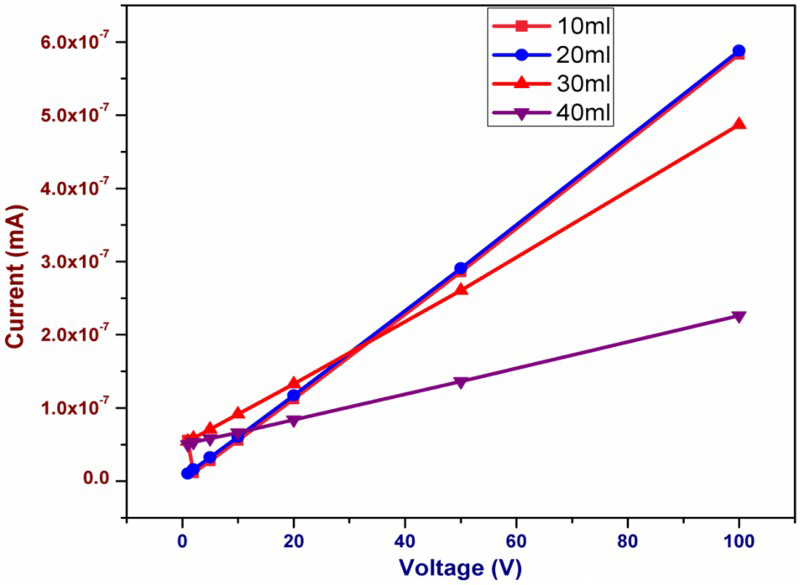
I–V characteristics
Conclusion
The CAO films are synthesised for different solvent volume ratios by spray pyrolysis method. The structural studies confirm the polycrystalline nature of CAO films with high texture. The preferential orientations are observed for (100) and (102) planes for different solvent volume ratios. When solvent volume increases, the average grain size also increases. The value of the energy gap decreases monotonically, and the electrical conductivity measured at ambient temperature increases with increasing the solvent volume. CAO films shows p type behaviour, and a direct band gap of ∼2·2 eV is observed. The CAO films are highly textured with high transmittance in the near IR range, which infers that all the visible wavelengths are strongly absorbed, and it can be used as the active layer in solar cells.
Footnotes
Acknowledgements
We wish to express our sincere thanks to the Department of Science and Technology, New Delhi, India, for their financial support [Project ID: INT/SWD/VINN/P-04/2011 and SR/FST/ETI-284/2011(C)]. We wish to acknowledge SASTRA University, Thanjavur, for extending infrastructural support to carry out this work.