
Abstract
Defect free diamond films have tremendous potential in a variety of areas including optoelectronics and have been the focus of several studies. Before diamond growth, a seeding treatment to substrate is mandatory, which itself is a source of contamination and degrades the quality of diamond. In the present study, diamond films without seeding treatment were grown on silicon using hot filament chemical vapour deposition. As a result of dry ultrasonic process, the diamond film with continuous layer was grown over unseeded substrate. At nucleation stage, carbon containing species were trapped by the uniformly created network of pits. Film grown at 2·0 vol.-% CH4 in H2 and substrate temperature of 850°C showed higher purity than that grown at 3·0 vol.-%CH4 in H2 and substrate temperature of 1000°C. Films grown over seedless substrates were also compared with those grown with seeding treatment.
Introduction
Diamond films synthesised by chemical vapour deposition (CVD) technique have potential in many applications due to their attractive properties, as indicated by a large number of publications on the subject.1, 2 Hot filament CVD (HFCVD) technique is commonly used to synthesise diamond films along with some other available techniques like microwave plasma CVD (MPCVD).3 However, HFCVD has the advantage to produce films over a large area4 and complex shapes.5
One common drawback of growing diamond films in HFCVD and MPCVD is the slow growth rate, as noted in published literature. There are some published reports indicating reasonable growth rate of diamond film;3, 6 however, increase in growth rate is mainly related to increased duration of the process. It is pertinent to mention here that in both the articles referred above, diamond films were grown by MPCVD. The problem becomes more serious when synthesising the film for shorter duration.
Diamond films grown by seeding process have higher defects, which not only appear on the back surface of the film but also protrude through the growing film, which afterward degrades the quality of diamond film. Hence, growing diamond films without seeding treatment in HFCVD is still a serious issue. Diamond films grown without seeding treatment have been the subject of abundant studies. We report here a new technique of dry ultrasonic treatment, which results in uniform seeding of the substrate. As the result of dry ultrasonic process, diamond films with full coverage are grown over substrate having no prior seeding treatment. The quality features of these films are close to the natural diamond.
Experimental
Boron doped p type silicon wafer having (100) orientation was used as the substrate material. Before charging the samples into the chemical reactor, surface treatment for two different durations was employed. A detailed description of dry ultrasonic process is given in our previous work.7, 8 For comparison purposes, diamond films were also grown over seeded substrates along with substrates prepared by dry ultrasonic process. The average grain size of diamond powder was 5 μm, while the duration for seeding treatment was 10 min.
Before the dry ultrasonic process, the substrates were dipped in 1∶1 HF solution for the duration of 2 min to remove any unwanted constituent. Face to face contact of front silicon surface and flat surface of a beaker was established and kept for the duration of 8 min (for sample 1) and 10 min (for sample 2). The substrate treated for 8 min would, hereinafter, be referred to as S1, while the substrate prepared for 10 min will be referred to as S2.
More or less identical process parameters for S1 are presented in Ref. 7, while that for S2 are presented in Ref. 8. In both samples, the total mass flowrate was 400 sccm, and chamber pressure was 80 torr. In S1, CH4 was 2·0 vol.-%, whereas it was 3·0 vol.-% for S2. Again, the substrate temperature for S1 was 850°C, while it was 1000°C for S2.
The synthesised films were characterised and analysed by field emission scanning electron microscopy and micro-Raman spectroscopy.
Results and discussion
Figure 1 shows SEM surface morphology of S1 and S2 before the deposition of diamond film, indicating the size of pits created due to dry ultrasonic process. As a result of ultrasonic agitation, pits were created over the surface of the substrate. The formation of pits for two different durations of agitation is shown in Fig. 1. It appears that network of pits looks slightly different. The bars of tissue paper along with some corroded regions are evident in S1. The pits in S1 are slightly smaller (∼600 nm) than those in the case of S2 (∼800 nm); this is mainly because of variation in the process duration.
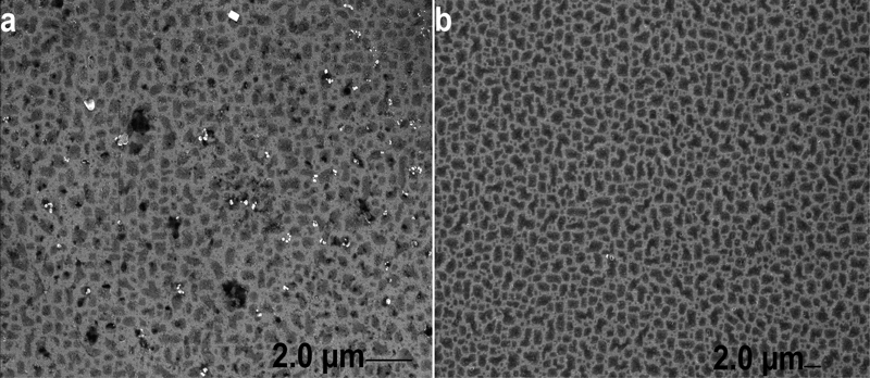
Surface images (SEM) of dry ultrasonic treated substrates for a S1 and b S2
The presence of pits on the surface of silicon helps to amalgamate carbon clusters and amorphous carbon during initial CVD process. Thus, once recrystallisation takes place in the amorphous region, it will act as a nucleation site for the growth of a diamond crystal.9 As a result of Coulomb force, pits have to attract carbon atoms during nucleation stage. The potential on the flat silicon surface is different from the potential of pits (along the edges and inside the pits). This is because charge accumulation is more inside the formed pits than that of original silicon surface. Hence, the localised potential (inside the pits) became the source of driving force for carbon containing species and thereon the formation of nuclei in those pits. Growth of diamond is initiated on these critical nuclei and proceeds uniformly in all directions by elongating diamond crystal. The graphitic phases nucleated at initial stage of the process are more likely electrically conductive, whereas disordered/ordered diamond phase grown at later stage is thermally conductive. In addition, the pits formed due to dry ultrasonic treatment exhibit rougher surface at localised regions of the silicon substrate. Consequently, these factors become favourable and contribute to initiate nucleation sites by trapping carbon containing species. Once, the critical nuclei are established, growth of diamond crystals proceeds on these sites.
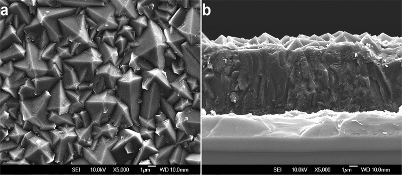
In S1, as shown in Fig. 2a, the morphology of diamond film is a triangular face {111} crystal (pyramidal shape), revealing an average grain size of 6 μm. The grain size is almost identical when observed via cross-section, which is shown in Fig. 2b. In these images, one can easily distinguish the grain size, as it grew in all directions.
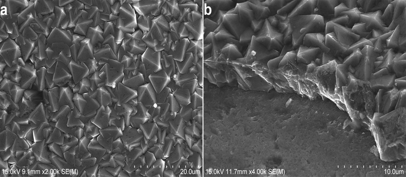
Images (SEM) of diamond films at 2 vol.-%CH4 grown over silicon without seeding showing a surface morphology and b tilted fracture cross-section
Figure 3 shows the surface morphology and cross-section image of S2. Surface structure of grown film reveals typical cubo-octahedron morphology, in which the average grain size of diamond is 9 μm (Fig. 3a), and it is almost identical when observed via SEM cross-section (Fig. 3b). Again, grains appear to be expanding in all directions, which grew from the surface of substrate. There is an available study for growing diamond film on unseeded silicon by HFCVD for 50 h resulting in the formation of a non-continuous diamond layer,10 whereas, in our case, as the result of dry ultrasonic treatment, full coverage of diamond film with reasonable growth rate is achieved.
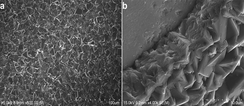
Images (SEM) of diamond films grown at 3 vol.-%CH4 over silicon without seeding showing a surface morphology and b tilted fracture cross-section
The results have also been compared with coating on bare substrate without ultrasonic treatment, simultaneously synthesised along with dry ultrasonic treated ones. Electron microscopy studies of diamond films grown over seeded samples are shown in Figs. 4 and 5. Surface morphology of these films (Figs. 4a and 5a) reveals identical morphology as in the case of S1 and S2, except accompanying secondary nucleation, twin crystals and grains’ interlocking/broken faces of crystals. Tilted fracture cross-sectional images of S1 and S2 are shown in Figs. 2b and 3b, which reveal slightly lower thickness than those films synthesised with seeding treatment (Figs. 4b and 5b). As a result of the tilt position, the precise measurement of film thickness for S1 and S2 is not possible. However, our earlier studies show that film synthesised with seeding treatment have higher growth rate (overall) compared to those grown without seeding treatment.7, 8 The higher growth rate for films synthesised at 3·0 vol.-%CH4 is due to an increase in methyl radicals.
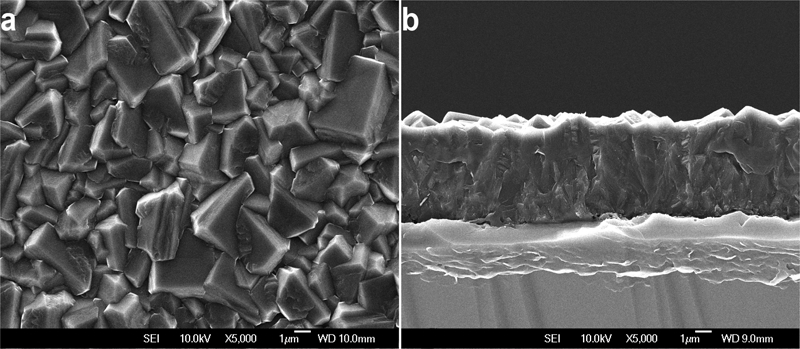
Images (SEM) of diamond films grown at 2 vol.-%CH4 over silicon with seeding treatment showing a surface morphology and b fracture cross-section
Images (SEM) of diamond films grown at 3 vol.-%CH4 over silicon with seeding treatment showing a surface morphology and b fracture cross-section
As an indication, Figs. 4b and 5b clearly show the presence of nanometric sized grains at the film/substrate interface, which become micrometre sized at the end of the process. The features of grains in these films look like cone shapes, which is not the case for films deposited without seeding treatment. Fracture cross-sectional images in Figs. 2b and 3b show that grains grew in cylindrical shape by maintaining surface/cross-section identical size and avoided nanosized particles at the interface. The higher growth rate in S2 is because of higher volume percentage of CH4 and vice versa.11
Figure 6 shows the Raman spectra of diamond films for S1 and S2 samples. Both samples show high purity diamond films, but better purity of diamond film is recorded in S1. This is because in Fig. 6, the wavenumber for S1 is at 1332·2 cm−1, while for S2, it is at 1332·5 cm−1. Therefore, the value of the wavenumber for S1 is closer to the value of the wavenumber of natural diamond, which is 1332·1 cm−1.12 The residual stress σ value is calculated by the relation ‘σ = −0·567 (v−v0) GPa’,13 and the σ calculated in diamond films for S1 and S2 are −0·0567 and −0·2268 GPa respectively. The lower value of σ for S1 indicates the higher level of purity within our experimental limits. Similarly, the full width at half maximum in the case of S1 is 3·5 cm−1, and for S2, it is 4·5 cm−1, whereas for natural diamond, it is 2·5 cm−1.12 In Fig. 6 (for S2), small peaks are seen in the range of wavenumber 1400–1550 cm−1. The intensity level of these peaks is quite low, and they completely vanish in the case of diamond film for S1. This indicates that due to higher volume percentage of CH4 in S2, non-diamond phases were also grown, which led into lower purity of diamond film grown at higher CH4 concentration. This is because amorphous carbon and graphite contents increased by increasing methyl radicals. In Fig. 6, the increase in the Raman signal seen in the spectrum of S1 from frequencies of 1800 cm−1 compared with spectrum of S1 actually reveals higher purity of diamond film for S1.
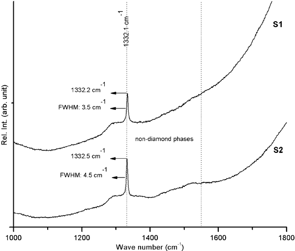
Raman spectra of diamond films deposited on silicon for S1 and S2
Conclusion
In this study, we have successfully shown the growth of high purity diamond films on seedless substrates. Seedless diamond films are also compared with the seeded one. The film grown at lower CH4 concentration exhibits higher purity compared with the one grown at higher CH4 concentration, and this is because of higher content of non-diamond phases associated with higher volume percentage of CH4. As the result of dry ultrasonic treatment, uniformly distributed pits are created over the silicon surface, which act as catching centres for incident carbon containing species. By increasing CH4 concentration from 2 to 3·0 vol.-%, diamond growth increases along with average grain size. The film prepared at 2·0 vol.-%CH4 shows pyramidal featured structure, whereas the film grown at 3·0 vol.-%CH4 reveals cubo-octahedron morphology. High purity diamond films are grown by avoiding incorporation of seeds, which themselves are sources of contamination.
Footnotes
Acknowledgements
Dr M. Ali wishes to thank ILO, CIIT, Islamabad Campus and IMR, Tohoku University, Japan, for providing financial support for the visit to Japan to characterise the samples. A part of this work was supported by TÜBİTAK under 2216-Postdoctoral Fellowship (Ref. no. B.02·1.TBT.0·06·01-216·01-677-6045).