
Abstract
Transparent conductive silicon doped zinc oxide (SZO, 3%Si) thin films are grown by direct current magnetron sputtering on glass substrates at room temperature. Experimental results show that the sputtering time has a significance impact on the growth rate, crystal quality and electrical properties of the films, and have little impact on the optical properties of the films. The growth rate decreases with the sputtering time. The resistivity of ZnO/Si films decreases as the sputtering time increases from 8 to 20 min. However, as the sputtering time increases further, the electrical resistivity increases instead. When other sputtering conditions are kept unchanged, it is found that the optimum sputtering time is 20 min and the achieved lowest resistivity is 4·92×10−4 Ω cm (sheet resistance = 11·5 Ω/sq for thickness 427·5 nm). The UV-vis transmission spectrum shows that all film samples present a transmission of above 90·0% in the visible range.
Keywords
Introduction
Transparent conductive oxides (TCOs) have been extensively utilised in electronic and optoelectronic industries due to their high electrical conductivity combined with high transmission in the visible and near-IR regions of the electromagnetic spectrum.1 Tin doped indium oxide (ITO) and fluorine doped tin oxide (FTO) are the most commonly used TCO. However, the cost of In and the high temperature needed for FTO deposition are limiting steps for the development of commercially available TCOs. Zinc oxide is II–IV wide bandgap (Eg = 3·37 eV) compound semiconductor with würtzite crystal structure. Its wide band gap is correlated with transparency in visible range.2 Therefore zinc oxide thin films become one of the most promising transparent conducting oxides for contemporaneous and emerging technologies for today's applications. Non-doped zinc oxide usually presents a high resistivity due to a low carrier concentration. The substitutional doping of ZnO with group III metals such as B, Al, Ga3, 4 (III group), Sn5 (IVA group) Zr, Ti6, 7 (IVB group) has already been widely reported and discussed in the literature. However, to the best of our group's knowledge, only few studies on Si dopants are reported8 – 10 and the sputtering method used is not a direct current (DC) magnetron sputtering. The interest of ZnO/Si materials was earlier noticed by Minami et al., indicating a minimum resistivity of 3·8×10−4 Ω cm for Si doped ZnO thin films deposited below 250°C using radiofrequency magnetron sputtering.9 More recently, Das et al.10 used the sequential pulsed laser deposition technique to grow highly transparent and c axis oriented thin films of Si doped ZnO on sapphire substrates. On doping with Si, the resistivity of the virgin ZnO thin films was found to decrease from ∼3·0×10−2 to 6·2×10−4 Ω cm and its bandgap increased from about 3·28 to 3·44 eV at different doping concentrations. Clatot et al.1 confirmed the promising performances (i.e. minimum resistivity value of 7·9×10−4 Ω cm) of Si doped ZnO thin films grown at 100°C using pulsed laser deposition.
The fabricating methods of doped ZnO thin films include: pulsed laser deposition,11 magnetron sputtering,12, 13 sol–gel method,14 magnetic electrodeposition method (reactive evaporation)15 and so on. As a frequently used method of film growth, the DC magnetron sputtering method has the advantages of simple process, low deposition temperature and so on, can fabricate uniform and large area films more easily than pulsed laser deposition method and can fabricate films with higher quality than sol–gel method.12 Thus, the research on the growth of thin film by magnetron sputtering method has more practical significance than by other deposition methods. In this study, ZnO/Si thin films are deposited on glasses by DC magnetron sputtering and its morphological, electrical and optical properties are investigated in detail. A silicon containing film on a silicon substrate helps prevent diffusion of the silicon into the substrate, because both the film and the substrate contain silicon, and therefore, has better stability and reliability. It is the objective of this work to determine basic properties of ZnO/Si thin films in dependence of sputter time, because the sputtering time plays an important role in determining the thickness and quality of film.16 – 18 This report may give an added impetus on the applications of this technologically important material and give newer alternatives to ITO and FTO in applications.
Experimental details
Substrate pretreatment
In the paper, substrates were 7059 glass with 0·15 mm thickness, which were cut into 60×30 mm samples, washed in 60°C acetone solution for 30 min with an ultrasonic washer to remove the organic solvents, dust and other impurities on glass surface, then dried in 40–45°C drying oven and then stored in a desiccator.
Sample preparation
The target was a high purity 99·99% ZnO–SiO2 crystal wafer (75 mm diameter and 3 mm thick) containing 97 wt-%ZnO and 3 wt-%of SiO2. It was produced from a mixture of commercial ZnO (99·99% purity), and SiO2 (99·99% purity) powders annealed at T = 1000°C for 48 h.
Silicon doped zinc oxide (SZO) films were deposited on to glass substrates by a JGP500C2-type DC magnetron sputtering system at room temperature. The base pressure in the chamber was 3·0×10−3 Pa. Sputtering gas was argon gas for industrial use and the depositions were performed in argon atmosphere of 4·0 Pa. The DC power and target substrate distance during the sputtering were fixed at 85 W and 60 mm respectively. Before sputtering, the target was presputtered (50 W DC power) for about 1 min with a shutter covering the target in order to remove the surface oxide layer. Then, the shutter was opened and sputtering process was started. In order to investigate the influence of deposition time on the properties of ZnO/Si films, the deposition time was fixed to 8, 11, 15, 20 and 25 min respectively. The deposition experiments were performed five times and five film samples (named A, B, C, D and E respectively) were obtained. During deposition, the argon gas flow was maintained at 30 cm3 min−1 and the substrate was not heated intentionally.
Sample measurements
The morphology of the film samples was investigated by scanning electron microscopy (SEM) with a Sirion 200 FEI microscope. Their structure and crystallinity were examined by X-ray diffraction (XRD) using a D8 Advance X-ray diffractometer with Cu Kα1
monochromatic radiation (λ = 0·15406 nm). The thickness of the film was measured by using a SGC-10 thin film thickness gauge with the measuring accuracy of less than 1 nm. This is a non-contact and non-destructive measurement based on the interference of light reflected from the film's top and its bottom surface, without sample pretreatment. Transmission spectra of the samples were recorded using a TU-1901 UV-vis spectrophotometer in the 300–900 nm wavelength range. The sheet resistance values
 at room temperature were achieved using the standard four-point probe method. If the film thickness d is uniform, the electrical resistivity ρ can then be determined using the relation
 .19,
20
.19,
20
Results and discussion
Structure and morphology of samples
SEM analysis
Figure 1 shows an SEM image (3×10⁴ times magnification) of the surface of ZnO/Si thin film samples deposited at different sputtering time, It can be verified that ZnO/Si thin films with a uniform crystal grain and flat surface morphology can be obtained by the DC magnetron sputtering method under present process conditions. But the crystal grain size of the sample changes with sputtering time, which starts to increase with increasing sputtering time and then decrease with a further increase in the sputtering time. For example, the crystal grain size of sample D is the greatest in all five samples. Sample D has the best compactness and crystalline among five samples. The change of the microstructures can be attributed to the change in sputtering time, because other preparation conditions are unchanged. Therefore, the microstructure of ZnO/Si thin films can be controlled by adjustment of the sputtering time.
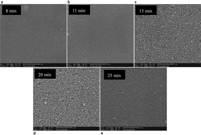
Scanning electron micrographs of ZnO/Si films deposited at different sputtering times: a sample A; b sample B; c sample C; d sample C; e sample C
XRD analysis
XRD measurements were performed after 3 months of aging in air and no any changes were found. Figure 2 shows the XRD patterns of ZnO/Si films deposited on glass substrates at various sputtering time (8, 11, 15, 20 and 25 min). It can be seen from Fig. 2 that besides the (002) diffraction peak of ZnO can be clearly observed, while no other obvious peaks are detected, indicating that the as prepared thin film samples have a good crystalline structure and textured with their c axis oriented perpendicular to the substrate. Especially, the diffraction peak of sample E in intensity is the highest in five samples. Figure 3 shows the partial enlarged XRD patterns of the samples with the 2θ in a range between 25 and 75°. It can be noted that two faint crystal orientation peaks of (100) and (004) can also be observed for samples C–E. However, these two diffraction peaks are almost not observed for samples B and A. Figures 2 and 3 also show that intensities of these diffraction peaks including (002), (100) and (004) are significantly enhanced with increasing sputtering time. The (004) diffraction peak of a film at 2θ ≈72·4°manifests that the films have high c axis preferred orientation.
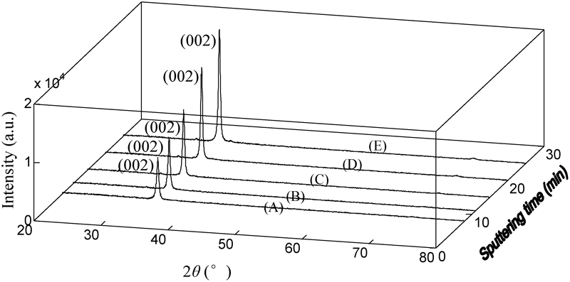
XRD patterns of ZnO/Si thin films deposited at different sputtering times (8, 11, 15, 20 and 25 min)
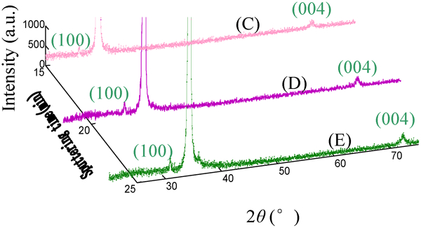
Partial enlarged XRD patterns of samples
In general, the intensity and the full width at half maximum (FWHM) of (002) peak can show the structural properties of the ZnO films. Figure 2 shows the intensity (002) peaks as a function of sputtering time. The peak intensity shows a marked increase with sputtering time. The FWHM firstly decreases from 0·36 to 0·28° when the sputtering time increases from 8 to 20 min, and then with further increasing sputtering time to 25 min, the FWHM increases gradually from 0·28 to 0·30°. Therefore, we can judge that the film deposited for 20 min has the highest crystallinity.
From the XRD patterns, it is also noted that the peak position corresponding to the ZnO (002) reflection is at lower 2θ values compared to the same diffraction peak of the standard ZnO crystals (2θ≈34·45°), which indicates that Si dopant induces a local lattice distortion thereby leading to larger lattice constants. The measured values of FWHM, 2θ of the (002) peak in XRD patterns and lattice constants for film samples deposited at different sputtering time are listed in Table 1. The 2θ value of sample C deposited at the sputtering time of 15 min is the largest one among five film samples and the closest to the diffraction peak position of standard ZnO crystal; thus, it has a minimum distortion. In the following discussion, we also know this sample with the smallest stress value.
Values of 2θ, full width at half maximum, lattice parameter, crystallite size and compressive stress for ZnO/Si films deposited at different sputtering times
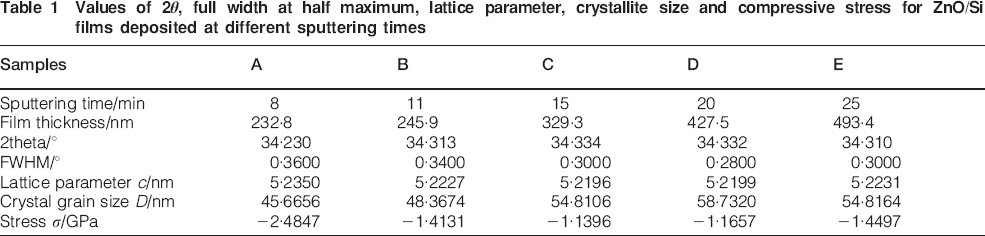
The average crystallite sizes of the film samples deposited at different target substrate distances are estimated from the peaks as shown in Fig. 2 based on Scherer's formula.21

A shift in the diffraction peak at (002) to a small angle is also detected in these Si doped thin films as compared with standard ZnO crystal as shown in Table 1, which reflects the lattice distortion induced due to the substitution of Si4+ for Zn2+. The crystal grain size of the samples is calculated by the Scherer's equation, and it is found to firstly increase and then decrease as the sputtering time is increased from 8 to 25 min. Sample D deposited at the sputtering time of 20 min has the largest crystallite size than the other four samples, which is coincided with the results obtained by SEM.
According to results presented in XRD patterns, for hexagonal crystals, the stress σ is in film samples is obtained using the following biaxial strain equation22


Effect of sputtering time on growth rate of ZnO/Si films
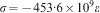
Figure 4 shows schematically the varying curve of film thickness and growth rate with sputtering time. As shown in Fig. 4, the film thickness increases from 232·8 to 493·7 nm with increasing sputtering time from 8 to 25 min, In contrast, the growth rates are found to decrease from 29·1 to 19·75 nm min−1.
Thickness and growth rate of Si/ZnO thin films versus sputtering time
With increasing sputtering time, the film thickness grows, but the growth rate is decreased, as can be seen clearly in Fig. 4. This can be explained by the fact briefly described below. At the beginning of the growth process, it is impossible to identify a coating layer on the rough substrate surface. After a period of sputtering time, column-like structures appear, a depletion layer is formed and material is transported to the growing interface by diffusion. With increasing deposition time, the columns grow, but the growth rate is decreased, as can be seen clearly on the micrographs, which is because smaller columns are included in the larger ones, and subsequently, they grow together, resulting in a slow growth rate. However, the individual column structures are kept separated by deep crevices. This behaviour follows the ‘survival of the fittest’ principle, which is also caused by geometric shadowing effects. This mechanism is proved by other model calculations described in Ref. 25. Furthermore, in the deposition process, the film structure was disturbed by nodular outgrowths, which are caused by dust particles and the shadowing effects. Therefore, the dust particles act as an inhibitor for film growth.
In Fig. 4, the variation of growth rate and film thickness can be divided into two regions at a boundary sputtering time of roughly 11 min: (1) region I where the growth rate decreases dramatically, but the film thickness increases slowly; (2) region II where the growth rate decreases slowly, but the film thickness increases dramatically. Three basic modes in thin film growth process are known: island (Volmer–Werber), layer (Frank–van der Merwe) and layer plus island (Stranski–Krastanov). Region I is a transition from the island growth mode to the layer plus island growth hybrid mode; this transient layer leads to a rapid decline of growth rate. It is clear that deposition time also influences upon the islands aggregation. In region II, the layer plus island growth mode plays the main role in the film growth. This process continues for some time and then steady state growth situation is reached. Thus, in region II, the film growth rate decreases slowly.
Electrical properties
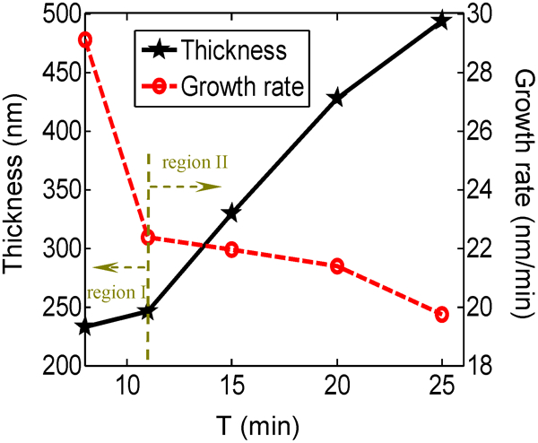
Figure 5 shows the relationship between resistivity and sputtering time, and also between sheet resistance and sputtering time. The variations in resistivities with the sputtering time show somewhat different behaviours as shown in Fig. 5. The variation process of resistivities is largely divided into two regions. In region I, which was up to the sputtering time of 20 min, the resistivities decrease with sputtering time from 1·33×10−3 to 4·92×10−4 Ω cm. However, in region II which was over the sputtering time of 20 min, the resistivities increase with sputtering time from 4·92×10−4 to 6·91×10−4 Ω cm.
Sheet resistance and resistivity of SiZnO thin films deposited at different sputtering times
In region I, the film thickness increases by island growth and layer plus island growth. In this process, the island density evidently decreases with deposition time, the grain size becomes large and the degree of crystallization increases. Yildiz et al. indicates that the potential barrier height in the films decreased with increasing grain size; on the contrary, the shrinkage of a grain size leads to an increment in the trapping states at a grain boundary. Trapping states are capable of trapping free carriers; as a consequence, more free carriers become immobilised as the density of trapping states increases.26 The decrease in the potential barrier height is also due to increase in crystallite size, resulting in diminishing charge carrier scattering at the grain boundaries. Hence, in region I, the improvement of crystallinity with sputtering time results in a resistivity lowering effect.
In region II, the film thickness increases mainly by layer plus island growth, the island density gradually tends to become stable with increasing sputtering time, the grain boundary density gradually tends to saturate and the crystallinity increases. Therefore, in region II with a high degree crystalline structure, the grain boundary scattering due to amorphous regions becomes subordinate, but the ionised impurity centres become an important factor for the carrier mobilities. This transition of the dominant electron scattering mechanisms from the grain boundary scattering in region I to the ionised impurity scattering in region II resulted in an decrease in the carrier mobilities with gradual increasing carrier concentrations (simultaneously producing ionised impurity scattering centres to trap the free electron carriers) in region II. Hence, in this region, the resistivity increases with increasing sputtering time.
Optical properties
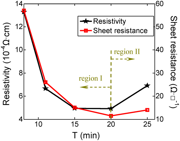
Figure 6 shows the optical transmission spectra as a function of the sputtering time and it is evident from the figure that the films are opaque for wavelength that is within the UV region and transmission starts at the visual spectrum. The average transmissions (including glass substrate) of five film samples in the visible range (400–800 nm) are 90·0161%, 93·2861%, 91·7289%, 91·5279% and 93·2119% respectively. These five film samples were produced at the sputtering time of 8, 11, 15, 20 and 25 min by keeping all other sputtering conditions unchanged respectively. The film thicknesses of these five samples are 232·8, 245·9, 329·3, 427·5 and 493·7 nm respectively. It is seen from these data that the film thickness has less impact on the optical transmission. The thickness of the film is directly related to the deposition time as we have previously noticed in the section on ‘Effect of sputtering time on the growth rate of ZnO/Si films’, which implies the impact of sputtering time on the overall transmission is very small. From the above data, we also see that the transmission varies up and down along the wavelength as a function of sputtering time. This is attributed to the change of film thickness due to sputtering time. The variation of film thickness leads to the periodical enhancement or weakening of transmission interference, namely, a transmission shock in the visible light band. It is easy to see from Fig. 6 that the cycle of the transmission oscillation along the wavelength has a certain relationship with the film thickness, and the greater the film thickness, the smaller the oscillation cycle.
Transmission spectra of SiZnO films deposited at different sputtering times versus wavelength
The optical absorption coefficient α was determined from transmission and film thickness data using the following equation

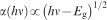
Square of absorption coefficient versus photon energy for ZnO/Si films deposited at different sputtering times
Conclusion
Highly transparent and conducting SZO film samples have been prepared at room temperature by DC magnetron sputtering on 7059 glass using different sputtering times. The effect of sputtering time on the structural, electrical and optical properties was studied. The achieved lowest resistivity is 4·92×10−4 Ω cm (sheet resistance = 11·5 Ω/sq for thickness 427·5 nm) and it is obtained for sputtering time of 20 min under an argon sputtering pressure of 4·0 Pa at a DC power of 85 W and a target substrate distance of 60 mm. All film samples present an overall transmission of over 90% in the visible spectra. Namely, the best sputtering time is found to be 20 min, while all other sputtering conditions (85 W, 4·0 Pa, argon gas flow 30 cm3 min−1, 60 mm) are maintained the same.
The films are found to show a preferential orientation in the (002) plane. According to the intensity and the FWHM of (002) peak, it is judged that the film deposited for 20 min has the highest crystallinity among five samples. The optical bandgap remains almost unchanged with sputtering time, whereas the absorption edge shifts slightly towards the lower energies with increasing sputtering time. The experimental results confirm that ZnO/Si will be one of very promising materials for fabricating high performance TCO thin films.
Footnotes
Acknowledgements
This work was supported by Shandong Province Natural Science Foundation (no. ZR2012FM001).