
Abstract
Considering the importance of electromagnetic shielding fillers in the advanced electromagnetic shielding material and the shortcomings of the current fillers in electrical and magnetic conductivity properties, a facile two-step electroless plating process, including coating nickel layer onto nano-SiO2 followed by coating another Ag layer onto SiO2/Ni obtained, was developed to fabricate electromagnetic shielding fillers in this study. The effects of SiO2 loadings on the thickness, density, magnetic permeability and electric conductivity of as obtained SiO2/Ni/Ag fillers have been investigated completely. The results indicated the thickness of Ni and Ag layer could be finely tuned by changing the content of SiO2 and SiO2/Ni during electroless plating processes. The optimised SiO2/Ni/Ag nanocomposites demonstrate high magnetic permeability and excellent electrical conductivity with 1·60×10−5 H m and 1·82×10−5 Ω m respectively. This method provides a facile and low cost strategy to fabricate nano-fillers for the polymer based electromagnetic shielding composite materials.
Introduction
With the rapid development of science, technology and electronic industry, more and more electronic equipment utilised generates a large amount of electromagnetic wave and radiation with different wavelength and frequency to the surroundings during their working, which leads to the non-ignorable electromagnetic interference among the electronic equipments.1–3 Especially, the electromagnetic interference is disastrous to some accurate electronic components since they are so sensitive to the electromagnetic interference around them that very low level electromagnetic interference may result into severe working improperly including misoperation, imaging disorder, and error data collecting. Besides the effects on the performance of electronic products, the electromagnetic interference produced by electromagnetic radiation may also lead to serious harms to human beings and other organisms, which is well known as electromagnetic pollution.4–6 Among all the strategies to reduce the electromagnetic pollution, using electromagnetic shielding materials in full-wave band with enhanced shielding effectiveness in the electric and electronic instruments has been proved to be one of the most effective ones.7–9
Depending on the frequency of the interference to the electromagnetic wave, different strategies have to be employed to achieve satisfactory electromagnetic shielding effect during the design and fabrication of the materials. If the frequency is high, the eddy current generated in low resistivity materials can be utilised to counteract the influence of external electromagnetic wave. However, if the frequency is rather low, high resistivity materials have to be applied to prevent the radiation of electromagnetic waves.10–13 The total shielding effectiveness (SE) of materials could be obtained by summing the individual contributions of the reflection (R), absorption (A) and multiple reflections (B) in dB as follows


Carbon series and metal coated series of fillers have been widely used in electromagnetic shielding materials for their high conductivities, low cost and facile processing properties.8,11,16–18 For instance, nano graphite was used as matrix to prepare nano silver flake graphite by a chemical silver plating process. The thickness of the nano silver flake graphite was 50 nm, and an electrical conductivity of nearly 106 S m−1 was achieved. 19 Wu and co-workers used carbon nanotubes as matrix to prepare the silver coated carbon nanotubes with good electrical conductivity through the way of chemical silver plating process. The prepared conductive adhesive exhibits an electrical resistivity as high as 2·2×10−3 Ω cm. 20 However, the magnetic conductivity at low frequency has rarely been considered in these reported materials. More recently, multi-walled carbon nanotubes (MWCNTs) were successfully plated by nickel (Ni) overlayer via an electroless plating strategy to further enhance the electrical performance. However, the resistivity of the Ni-MWCNT composites obtained is relatively large although its surface conductivity is up to 4·2×10−7 S cm−1. 16
In order to achieve both high magnetic and electric conducting performance, this paper designed and fabricated a kind of novel electromagnetic shielding nanocomposite fillers with advanced electromagnetic shielding effectiveness via a facile two-step electroless plating strategy. 21 First, a thin nickel layer was uniformly coated on the surface of SiO2 nanoparticles (denoted as SiO2/Ni) to improve the magnetic permeability. Second, the silver overlayer was once again coated onto the surface of SiO2/Ni coating (denoted as SiO2/Ni/Ag) with the similar process to further enhance the electric conductivity. Interestingly, it is found that the magnetic and electric conductivities could be finely controlled via adjusting the composition of the nanocomposites. As a result, such novel nanocomposite fillers could deliver excellent magnetic and electric conductivity properties.
Experiment
Material synthesis
All of the reagents were supplied by Sigma–Aldrich with analytical grade and used as received. A two-step electroless plating method was involved to prepare SiO2/Ni/Ag nanocomposites as follows. First, a thin and uniform nickel-phosphorus alloy coating is plated onto the surface of SiO2 nanoparticles (denoted as SiO2/Ni) in an electroless solution to improve their magnetic permeability. Second, thin silver overlayer is once again coated onto the surface of above SiO2/Ni particles (denoted as SiO2/Ni/Ag) to further improve their electric conductivity. It must be noticed that the pristine SiO2 nanosparticles should be corroded by dilute HF solution (0·5 mol L−1) before the electroless plating to improve the absorption between SiO2 particles and metal ion (Ni2+ and Ag+). A typical synthesis process of SiO2/Ni nanocomposites was carried out in the following procedure. First, the SiO2 powder with a diameter of 50 nm was dispersed in an electroless solution with the assistance of ultrasonication for 5 min. Then the suspension was transferred to a water-bath to carry out the electroless plating under vigorous stirring at 93°C. The electroless solution with a pH value of 5 was pre-prepared by dissolving 25 g of NiSO4.6H2O, 27 g of NaH2PO4, 20 g of CH3COONa, 15 g of lactic acid and 2 g of propionic acid in 1 L of deionised water. During the coating of the silver layer, a silver ammonia solution containing 7 g L−1 of AgNO3 and 40 mL L−1 of NH3.H2O was employed in the following procedure. The nickel coated SiO2 obtained above was dispersed in an anhydrous ethanol solution containing 20 mL L−1 HCHO with ultrasonication for 30 min to form a uniform suspension. Then the pre-prepared silver ammonia solution was added into the above suspension drop wisely under vigorous stirring. During the process of plating, the temperature was controlled at 28°C and pH was adjusted to 13 with NaOH solution (2 mol L−1).
Material characterisation
X-ray diffraction (XRD) patterns were carried out on a Bruker D8 Advanced X-ray diffractometer with Ni filtered Cu Kα radiation (λ = 1·5406 Å) at a voltage of 40 kV and a current of 40 mA. Field emission scanning electron microscope (FESEM) images were acquired on a JEOL JSM-6700F microscope operated at 5 kV. X-ray Energy dispersive spectroscopy (EDS) was performed on a SEM-X-ray microanalysis spectrometer (JEOL JED-2300) at an accelerating voltage of 15 kV. Transmission electron microscope (TEM) images were taken on JEOL JEM-2010 and JEOL JEM-2100F microscopes. The diameter distribution was carried out on a laser particle analyser (Mastersizer 3000). Electric conductivity properties were taken by HP RLC4284A Bridge. Magnetic properties were taken by TF-CIB static hysteresis loop measurement instrument.
Results and discussion
The morphology and structure of the pristine SiO2 powder and as prepared nickel coated SiO2 (denoted as SiO2/Ni) were characterised with FESEM. As shown in Fig. 1a, the pristine SiO2 nanoparticles aggregate with each other severely with less than 100 nm in diameter. However, after coated by nickel nanocoatings, the diameter of the nano-SiO2/Ni particles is improved to round 140 nm with well mono-dispersed spherical structure (Fig. 1b). In addition, EDS results shown in Fig. 1c and d further confirm that the nickel coating has been plated onto the surface of SiO2 particles successfully. According to the EDS analysis in Fig. 1c, only Si and O elements have been detected, indicating the high purity of the pristine SiO2 fillers. However, after coated by nickel layers, besides of Si and O elements, Ni and P elements could also be prominently detected from the EDS analysis, in which the P element should originate from the nickel phosphorus alloy layer. More importantly, the weight percentage of Ni and P elements are round 85·34 and 13·18% respectively, suggesting the amount of nickel phosphorus alloy layer is much higher than that of the SiO2 substrate. Therefore, the nickel coated nano-SiO2 is much larger than the pristine SiO2 in size. Furthermore, the thickness of nickel coating layer was evaluated by TEM (inset of Fig. 1b). Clearly, the as prepared SiO2/Ni nanocomposites present the core shell structures with the total size of about 130 nm and the shell thickness of nickel coating layer of round 50 nm, which is also confirmed by their diameter distribution. As shown in Fig. 2a, the diameter of pristine SiO2 particles is about 60 nm. However, after coated by nickel layer, the diameter of SiO2/Ni composites is increased to round 130 nm (Fig. 2b), which agrees well with above FESEM and TEM observations.
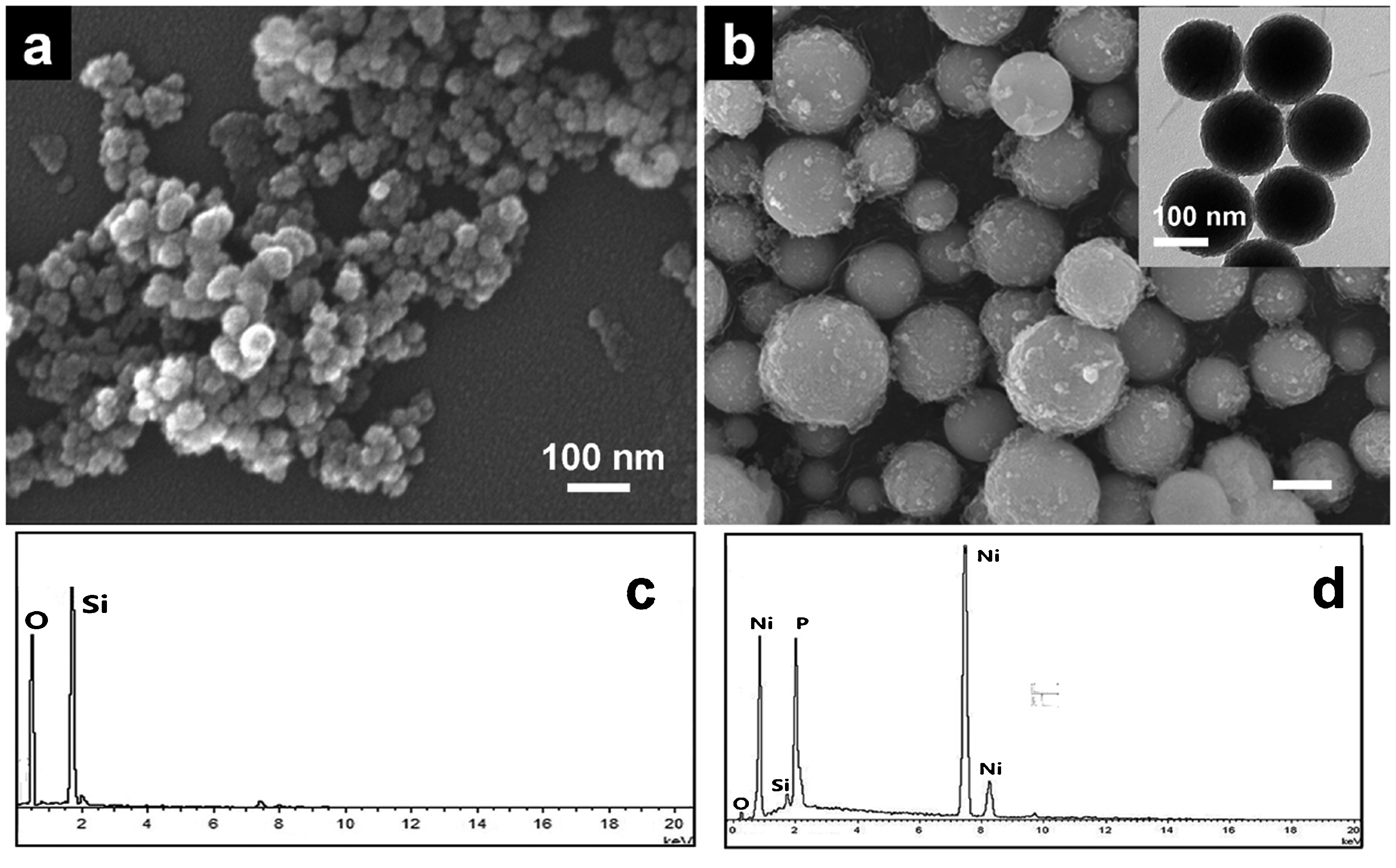
FESEM and EDS of a, c SiO2 and b, d SiO2/Ni, inset of b is TEM images of SiO2/Ni
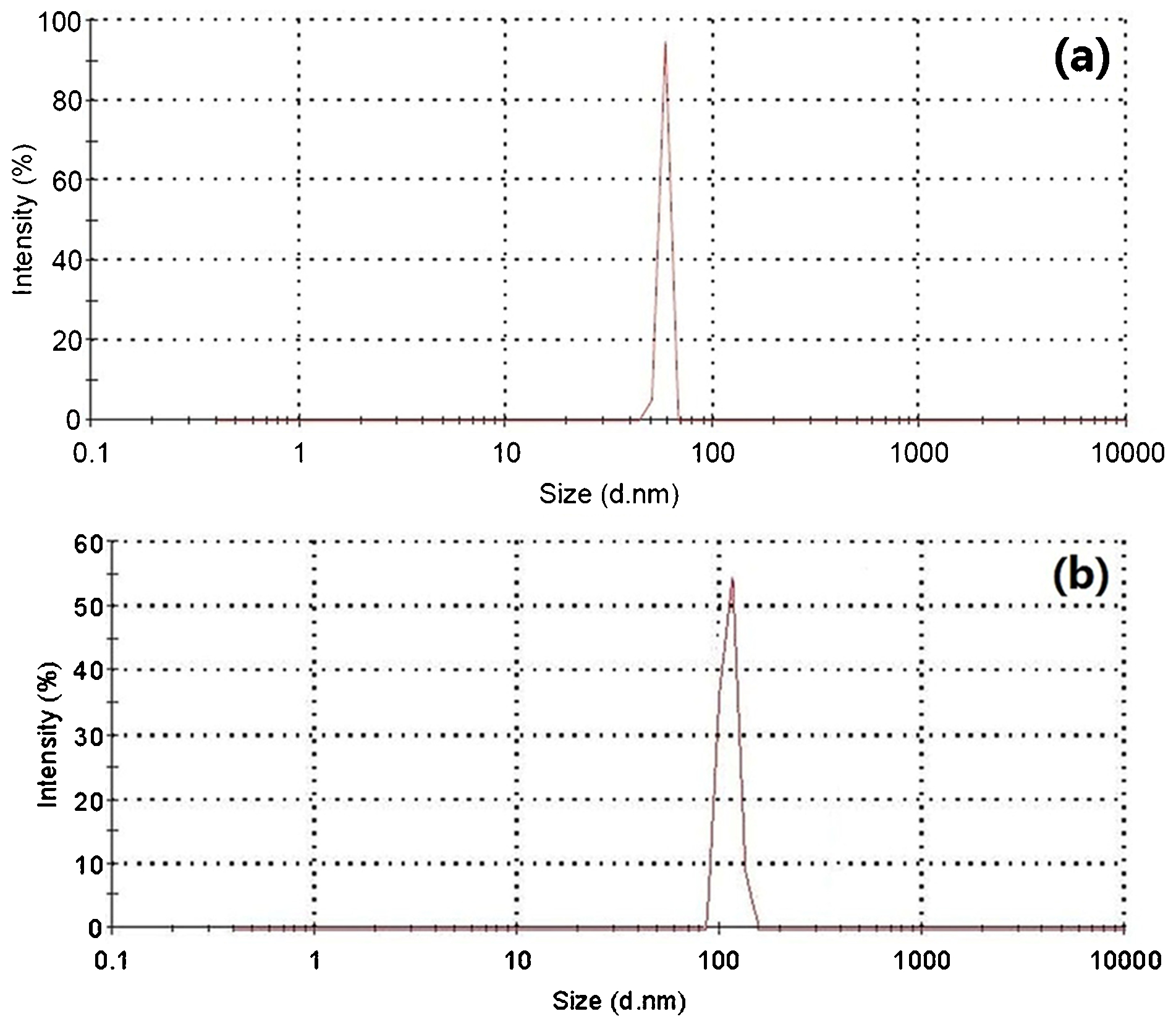
Diameter distribution of a pristine SiO2 and b nickel coated SiO
The crystallographic structure of pristine SiO2 and as prepared SiO2/Ni composites was examined by powder XRD as shown in Fig. 3a. The pristine SiO2 powder only presents one broad diffraction peak centred at around 22°, which can be well assigned to the cristobalite SiO2 phase (JCPDS card no. 39-1425). 22 After the electroless plating process, however, a large amount of nickel phosphorus alloy coating layer has been coated onto the surface of the cristobalite SiO2 particles. As a result the SiO2/Ni powder demonstrates two strong diffraction peaks at about 44 and 60°, which corresponds to the (111) and (200) crystal planes of nickel phosphorus alloy respectively. 16
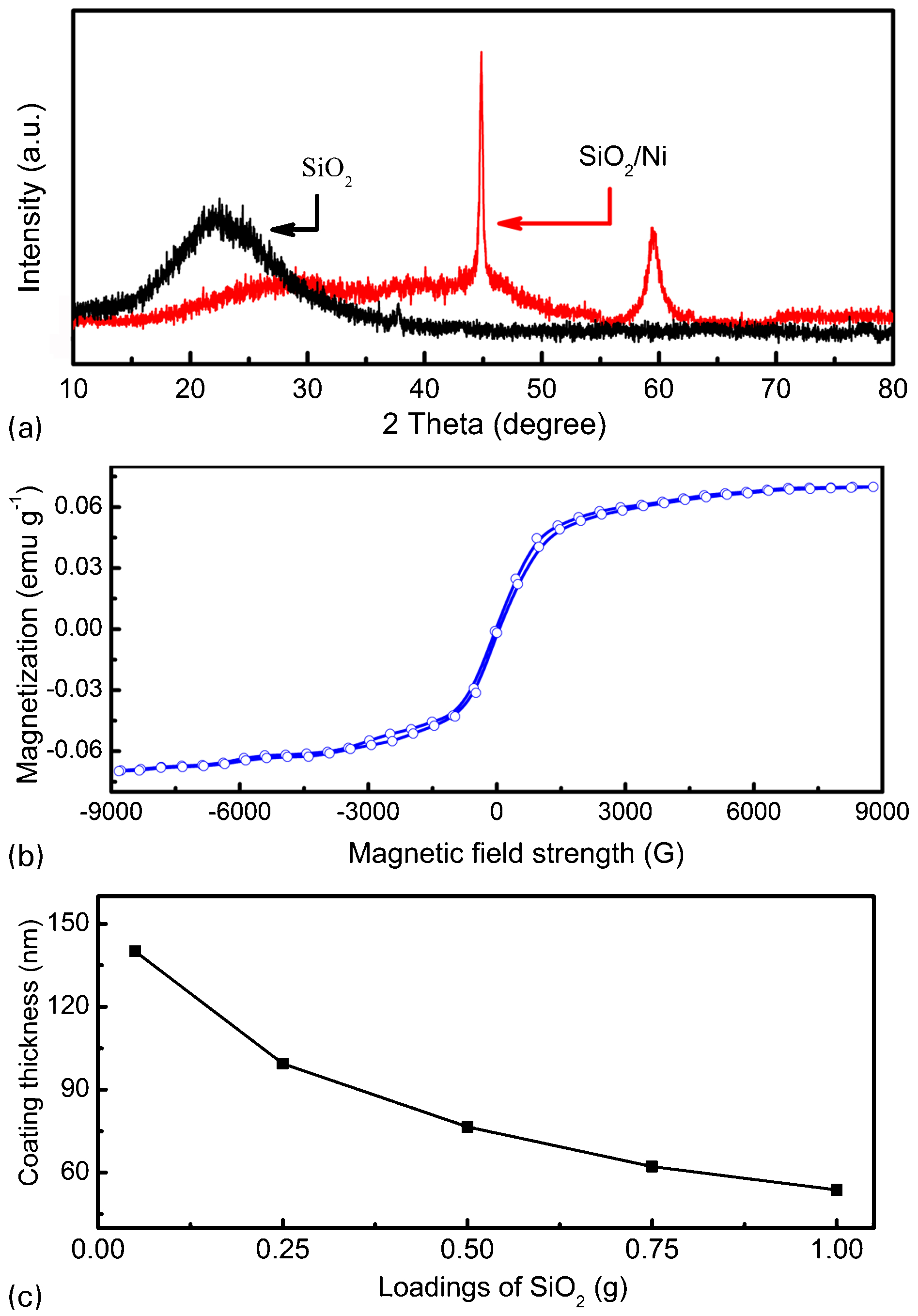
a XRD pattern of SiO2 and SiO2/Ni nanocomposites, b hysteresis loop of SiO2/Ni and c effects of SiO2 loadings on coating thickness of nickel layer
We further tested the magnetic hysteresis loop of as prepared SiO2/Ni/Ag fillers as shown in Fig. 3b. Obviously, the magnetic hysteresis loop of as prepared SiO2/Ni/Ag composites delivers a typical S-shaped curve through the zero. In the first quadrant, the magnetization increases sharply at first and then flats out with the growth of positive and external magnetic field. In the third quadrant, correspondingly, it decreases sharply at first and then also flats out with the growth of negative and external magnetic field. That should be attributed to the nickel phosphorus alloy coatings on the surface of nano SiO2 after the electroless plating process. When electrons outside the nucleus of nickel atoms are exposed in the external magnetic field, self-spin of these electrons would lead to the spin magnetic moment. As a result, nickel coated SiO2 nanoparticles are continuously magnetized by the external magnetic field with the property of remarkable ferromagnetism. That may explain the excellent ferromagnetic performance observed in the SiO2/Ni/Ag nanocomposites.
The effects of SiO2 dosage on the thickness of nickel coating were investigated as well as shown in Fig. 3c. The thickness of nickel coating is decreased sharply from 27·3 to 4·85 nm with the increasing SiO2 dosage during the electroless plating process. Therefore, the SiO2 loadings should be finely controlled to obtain the SiO2/Ni composites with expected coating thickness. In order to further improve the electronic conductivity of SiO2/Ni nanocomposites, a thin silver overlayer is coated on the surface of SiO2/Ni (denoted as SiO2/Ni/Ag) via another electroless plating process. As shown in Fig. 4a, mono-dispersed spherical structure of the SiO2/Ni/Ag nanocomposites with a diameter of about 400 nm can be observed clearly. In addition, the surface of SiO2/Ni/Ag becomes very coarse due to the coating of silver plating. EDS analysis (inset of Fig. 4a) discloses that the surface overlayer is mainly silver, indicating the successful silver coating process. The XRD pattern of SiO2/Ni/Ag was shown in Fig. 4b. Four distinct diffraction peaks can be observed at round 38·16, 44·38, 64·52 and 77·42°,1,3 which can be well assigned to the crystal silver phase (JCPDS card no. 04-0783).23–25 That is to say, the coated silver layer is crystallized in face centred cubic structure. The diffraction peak at about 60° should be ascribed to the diffraction peak of nickel.
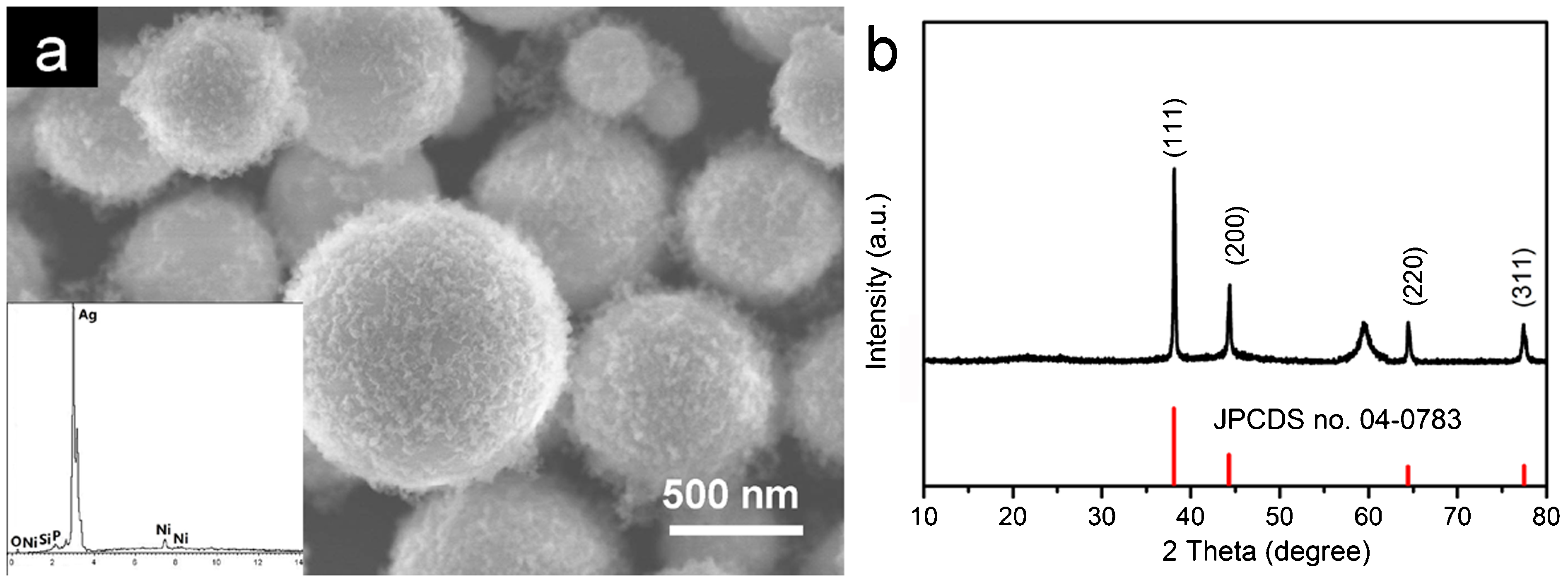
a FESEM image and b XRD pattern of SiO2/Ni/Ag, inset of a is its EDS
Meanwhile, the loading of SiO2/Ni substrate is further optimised to evaluate the plating density of composites and its thickness. As shown in Fig. 5a, the density and the thickness of the silver plating both decrease sharply with the SiO2/Ni loading increasing from 0·05 to 1·0 g. With the increasing SiO2/Ni loading, the thickness of silver overlayer on the substrate will be thinner and thinner since the concentration of silver ion in solution is constant. As a result, the silver overlayer density of SiO2/Ni/Ag nanocomposites becomes looser and looser. The resistivity of SiO2/Ni/Ag nanocomposites is evaluated under various SiO2/Ni loadings as shown in Fig. 5b. When the loading capacity of SiO2/Ni substrate increases from 0·05 to 0·75 g, the resistivity of as prepared SiO2/Ni/Ag nanocomposites presents a slightly ascendant trend. However, once the loading of the SiO2/Ni substrate is over 0·75 g, the resistivity of the SiO2/Ni/Ag nanocomposites increases sharply. It was well known that silver overlay owns excellent electrical conductivity. The more the loading of SiO2/Ni substrate is, the thinner the silver coating is obtained, and the lower electrical conductivity of the final composites displays. The optimized electrical conductivity of as prepared SiO2/Ni/Ag nanocomposites is obtained as 1·82×10−5 Ω m. Besides the electrical conductivity, the magnetic permeability is another important index for the electromagnetic shielding materials. Figure 5c shows the effects of SiO2 loading capacity on the magnetic field strength of SiO2/Ni/Ag nanocomposites. As can be observed, when the amount of SiO2 substrate is increasing slowly from 0·05, 0·10, 0·15 to 0·20 g, the corresponding magnetisation curve rises up sharply initially and then increases slowly until a horizontal plateau is arrived. Owing to the increase of the intensity of the external magnetic field, SiO2/Ni/Ag nanocomposites are further magnetised to reach the saturation magnetisation. However, when the amount of SiO2 is over 0·25 g, the corresponding magnetisation value arises up sharply initially. However, due to the lower thickness of nickel layer (Fig. 3c), the magnetisation of the composites suddenly drops to −125 A m−1 sharply and finally keeps a stable value of as high as −143 A m−1 when the magnetic field strength reaches about 3000 G. That may be attributed to the thin and imperfect coating of nickel layer formed at such high SiO2 loading capacity. Silver shows diamagnetism, and will not be magnetised. When the strength of the external magnetic field is lowered, the combined magnetic moment in the nickel shell is greater than the magnetic moment in the SiO2 core. The direction of the integrity of the combination of the magnetic moment is the same as the direction of the external magnetic field showing the magnetism. Therefore, it is magnetised gradually. Oppositely, when the strength of the external magnetic field is larger, the combined magnetic moment in the nickel layer is lesser than the magnetic moment in the silica. The direction of the integrity of the combination of the magnetic moment is opposite to the direction of the external magnetic field showing the diamagnetism. As a result it cannot be magnetised greatly. In other words, with the increasing of SiO2 substrate loading, nickel phosphorus alloy layer on the surface of SiO2 becomes very thin and incomplete. Therefore, when the strength of the external magnetic field is low, it can be easily magnetized to show magnetism. However, if the strength of the external magnetic field is very large, it cannot be magnetized. In this paper, the magnetic permeability of as prepared SiO2/Ni/Ag is 1·60×10−5 H m−1.
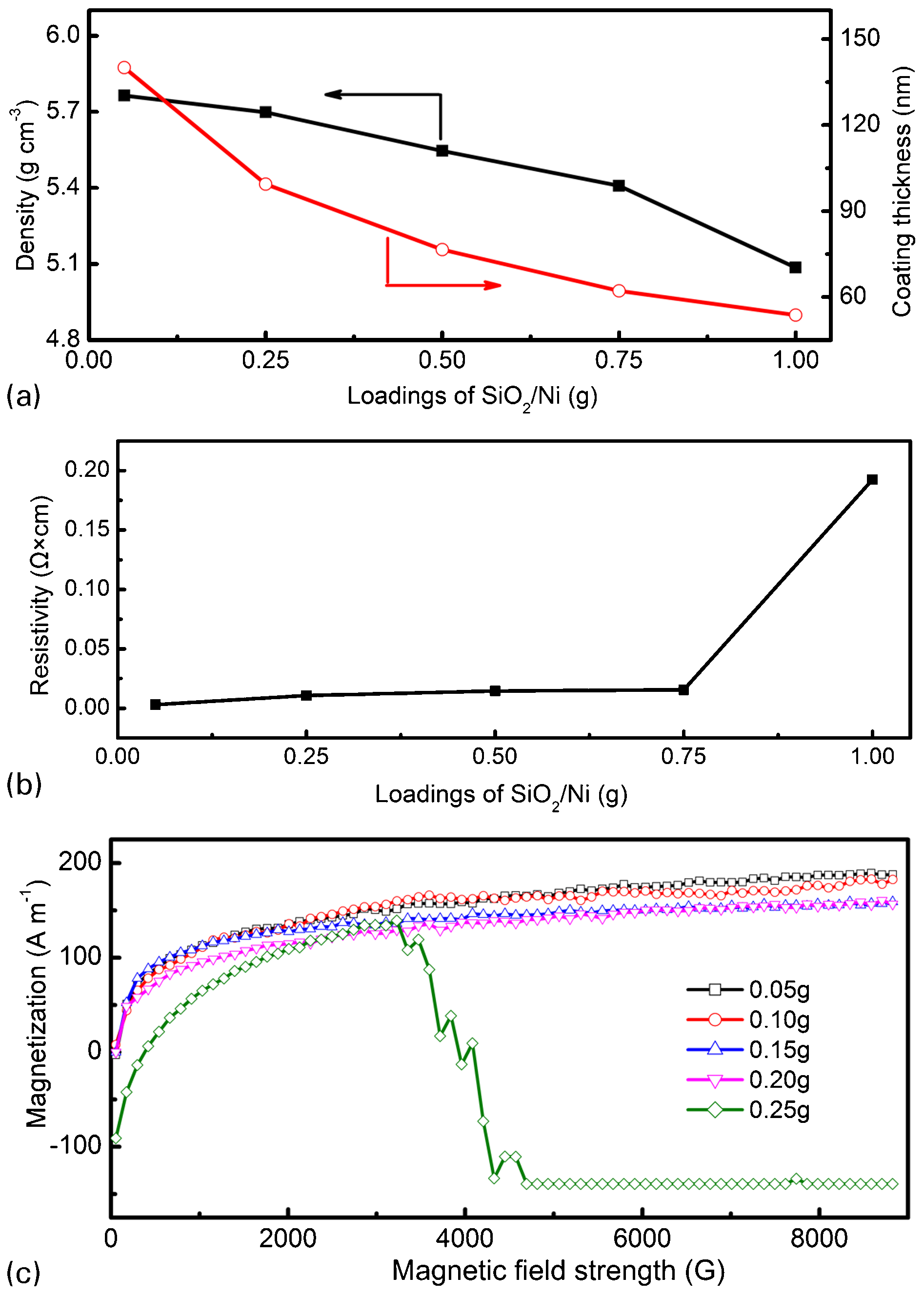
Effects of SiO2/Ni loadings on a density and coating thickness, b resistivity and c magnetic field strength of SiO2/Ni/Ag nanocomposites
Conclusion
A series of electromagnetic shielding fillers with well designed core shell nanostructure were fabricated via a facile two-step electroless plating process in present work. The FESEM, TEM images and EDS confirm that the nickel layer and silver layer have been plated onto the nano-SiO2 surface. The effects of SiO2 loadings on the thickness, density, magnetic permeability and electric conductivity of as obtained SiO2/Ni/Ag fillers have been investigated completely. The coating density and thickness of the final SiO2/Ni/Ag both increase gradually through decreasing the loading content of substrate. The obtained nanocomposite fillers demonstrate excellent magnetic and electric conductivity properties depending on their composition. The magnetic permeability and the electrical conductivity of optimised SiO2/Ni/Ag nanocomposites were obtained as 1·60×10−5 H m−1 and 1·82×10−5 Ω m respectively. The excellent electromagnetic shielding capability allows them to be utilized to fabricate electromagnetic shielding composites.