
Abstract
Highly crystalline cadmium doped lead sulphide (PbS:Cd) thin films with different Cd doping concentrations (0, 2, 4, 6 and 8 at-%) were fabricated on glass substrates using spray pyrolysis technique. The X-ray diffraction (XRD) studies revealed that all the films exhibit face centred cubic structure with a preferential orientation along the (2 0 0) plane irrespective of Cd doping concentration. Optical studies showed that the band gap of doped films vary between 1·96 and 2·12 eV with increasing Cd content and the film coated with 6 at-% Cd dopant has a maximum transmittance of nearly equal to 77%. Electrical studies revealed that the film coated with 6 at-%Cd dopant has a maximum conductivity of 12·67×10−1 Ω cm−1. The obtained results infer that the PbS:Cd film coated with 6 at-%Cd dopant has better structural, morphological, optical and electrical properties.
Keywords
Introduction
Semiconducting materials with outstanding electrical and optical properties finds application in light emitting diodes, single electron and field effect thin film transistors.1–3 II–VI and IV–VI group semiconducting materials are mostly studied since they can be easily synthesised either in particle form or in thin film form. Lead sulphide (PbS) a direct band gap A4B6 semiconductor has a narrow band gap of 0·41 eV at room temperature. 4 The band gap of PbS can be varied significantly by changing the grain size and there are reports of opening the band gap to as high as 2·5 eV from its bulk value by decreasing the grain size to the nanoregime. 5 This notable change in band gap is a result of small effective masses of electrons (me) and holes (mh); me = mh = 0·09 mo, and the large exciton Bohr radius (18 nm). 6 PbS films possess excellent solar control characteristics than metallic films when deposited on glass substrates. 7 PbS thin films find potential applications in photoresistors, diode lasers, humidity and temperature sensors. 8 To utilise PbS thin films for optoelectronic applications, low resistivity and high transparency is required. To enhance the electrical and optical properties of PbS films, doping has been tried by different investigators and enhanced physical properties has been achieved.9–13 To obtain PbS thin films with wide optical band gap and improved electrical conductivity, other suitable dopant which does not alter the PbS crystal structure should be identified. Cadmium sulphide (CdS) is an important wide band gap semiconductor with Bohr atomic radius of 2·4 nm and direct band gap of 2·43 eV. 14 Hence, it is expected that the homogeneous composing of CdS and PbS allow intermediated optical and electrical properties between them, making PbS:Cd attractive for various optoelectronic device applications. It is well known that cadmium is an important transition metal element having an ionic radius of 0·97 Å which is slightly less than that of Pb2+ (1·19 Å) and hence, Cd2+ can easily penetrate into PbS crystal lattice and substitute Pb2+ positions in the crystal, which can tune its energy band gap and lattice parameters suitable for optoelectronic applications. There are earlier reports showing the enhancement in the electrical and optical properties of mixed films of PbS and CdS.15,16 Recently, Thangavel et al. 17 showed that wide band gap can be obtained for Cd doped PbS thin films while annealing. Increased band gap values for PbS films fabricated by spray pyrolysis technique were also reported by Suhail 18 It is known that the concentration of dopant play a vital role in enhancing the properties of semiconducting thin films. Therefore, in the present study, the effect of doping concentration on the physical properties of Cd doped lead sulphide (PbS:Cd) thin films have been studied and the results are presented. PbS:Cd thin films were fabricated on glass substrates at 400°C by cost effective spray pyrolysis technique with different Cd doping concentrations (0, 2, 4, 6 and 8 at-%). Spray pyrolysis technique is adopted here as this method is simple and suitable for large area deposition. Moreover, the film growth can be easily controlled by varying the preparative parameters such as spray rate, substrate temperature, solution concentration, nozzle frequency, etc. 19
Experimental
To prepare PbS:Cd thin films, lead nitrate [Pb(NO3)2] (0·025M), thiourea [CS(NH2)2] (0·025M) and cadmium acetate [Cd(CH3COO)2], all of analytical reagent grade (Sigma make) were used as source precursors for Pb, S and Cd respectively. The starting solution was prepared by dissolving the precursor salts in deionised water (50 ml in volume). The precursor solution when sprayed over hot glass substrates kept at 400°C, pyrolytic decomposition takes place resulting in the formation of PbS thin films. X-ray diffraction (XRD) patterns were obtained using a X-ray diffractometer (PANalytical, PW 340/60 X'pert PRO) having Cu Kα radiation of wavelength 1·5406 Å as the source. Scanning electron microscope (HITACHI S-3000H) is used the surface morphology of the films. A PerkinElmer double beam UV–Vis–NIR spectrophotometer (LAMBDA 35) is used to perform optical studies. The electrical studies of the films were carried out using two-point probe method.
Results and discussion
Structural studies
Figure 1 shows the XRD patterns of the undoped and Cd doped PbS films. The diffraction peaks are well fitted with face centred cubic structure of galena PbS. All the doped PbS films have preferential orientation along the (2 0 0) plane as that of the galena film irrespective of Cd doping level, indicating that the incorporation of Cd into the Pb sites does not alter the preferential growth. Other weak peaks observed are associated with the (1 1 1), (2 2 0), (3 1 1) and (4 0 0) planes of PbS cubic structure (JCPDS Card No. 65-0135). The preferential orientation of (2 0 0) plane obtained here exactly matches with the results reported by Seghaier et al. and Raniero et al.20,21 for PbS thin films grown by chemical bath deposition technique. No secondary peaks related to CdS are observed in the patterns, indicating the purity of the films. This clearly shows that Cd2+ ions are well dissolved in the PbS lattice since the ionic radius of Cd2+ is less than that of Pb2+.
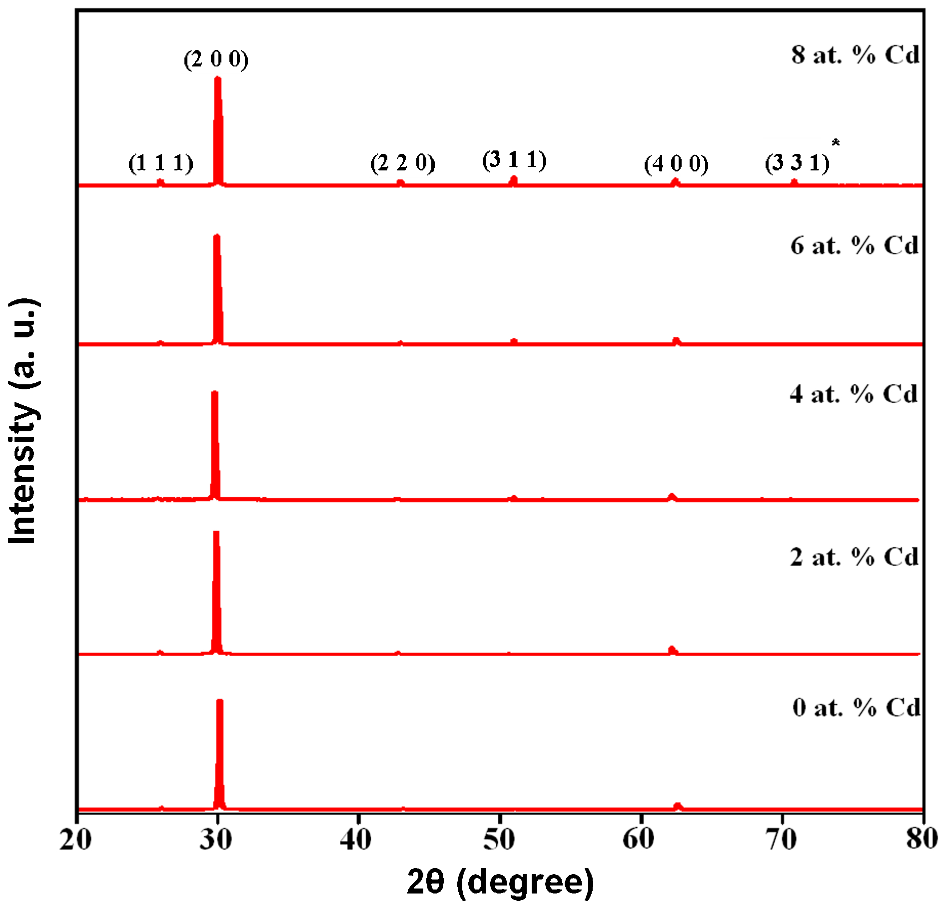
X-ray diffraction (XRD) patterns of galena and Cd doped PbS films
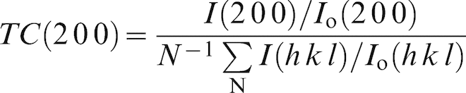
The texture coefficient (TC) of the undoped and doped PbS films corresponding to the (2 0 0) plane is calculated using the formula
22
Structural and electrical parameters of PbS:Cd thin films
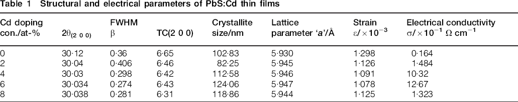
The obtained value of ‘a’ for the undoped film exactly matches with the standard data (JCPDS Card No. 65-0135). It can be seen that the lattice parameter value increases monotonically with increasing Cd concentration up to 6 at-% doping level. This unit cell volume expansion is due to the ionic radii mismatch (whether +ve or −ve) between Pb2+ and Cd2+ ions. Owing to this volume expansion, strain has been induced in the films and hence, crystalline qualities are deteriorated. The increased crystallite size values observed for these films strongly supports for this unit cell volume expansion. As the doping concentration is increased further, a slight decrement in ‘a’ value is observed and this volume contraction might be due to the formation of CdS sites in the host PbS lattice. The formation of CdS site is well acknowledged by the presence of (3 3 1) plane (Fig. 1, represented by asterisk) corresponding to the cubic CdS.
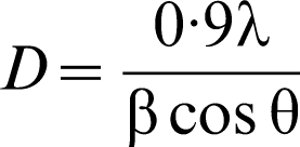
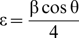
The strain (ϵ) related to lattice misfit due to growing conditions is calculated using the relation
SEM analysis
Figure 2 shows the SEM images of the undoped and Cd doped PbS thin films. It can be clearly seen that all the films were covered with grains uniformly distributed throughout the substrate surface. Few patches of interconnected grains are also visible in the morphology of the undoped sample (Fig. 2a). It is observed that surface morphologies of the doped films changes considerably with Cd doping concentrations (Fig. 2b–e). With 2 at-% Cd dopant, the surface modifies with small cuboids (Fig. 2b) without any devoids or holes. Traces of few interconnected cuboids are also visible. With 4 at-%Cd dopant, the surface modifies with cubes of different sizes (Fig. 2c). No interconnected grains are visible and traces of few pyramidal shaped grains are observed. As the dopant concentration is increased further, the surface modifies with cubes of almost equal size. More pyramidal shaped grains are visible for the film coated with 6 at-%Cd (Fig. 2d). Moreover, this sample also displays a uniform grain size distribution compared to the other doped samples. With further increase in the Cd content (8 at-%), the surface deteriorates largely with minimisation of cubical shaped grains (Fig. 2e). Needle shaped grains with traces of few empty sites are also visible in this film. These results infer that the PbS film morphology modifies with Cd doping and the film coated with 6 at-%Cd dopant has better morphological properties.
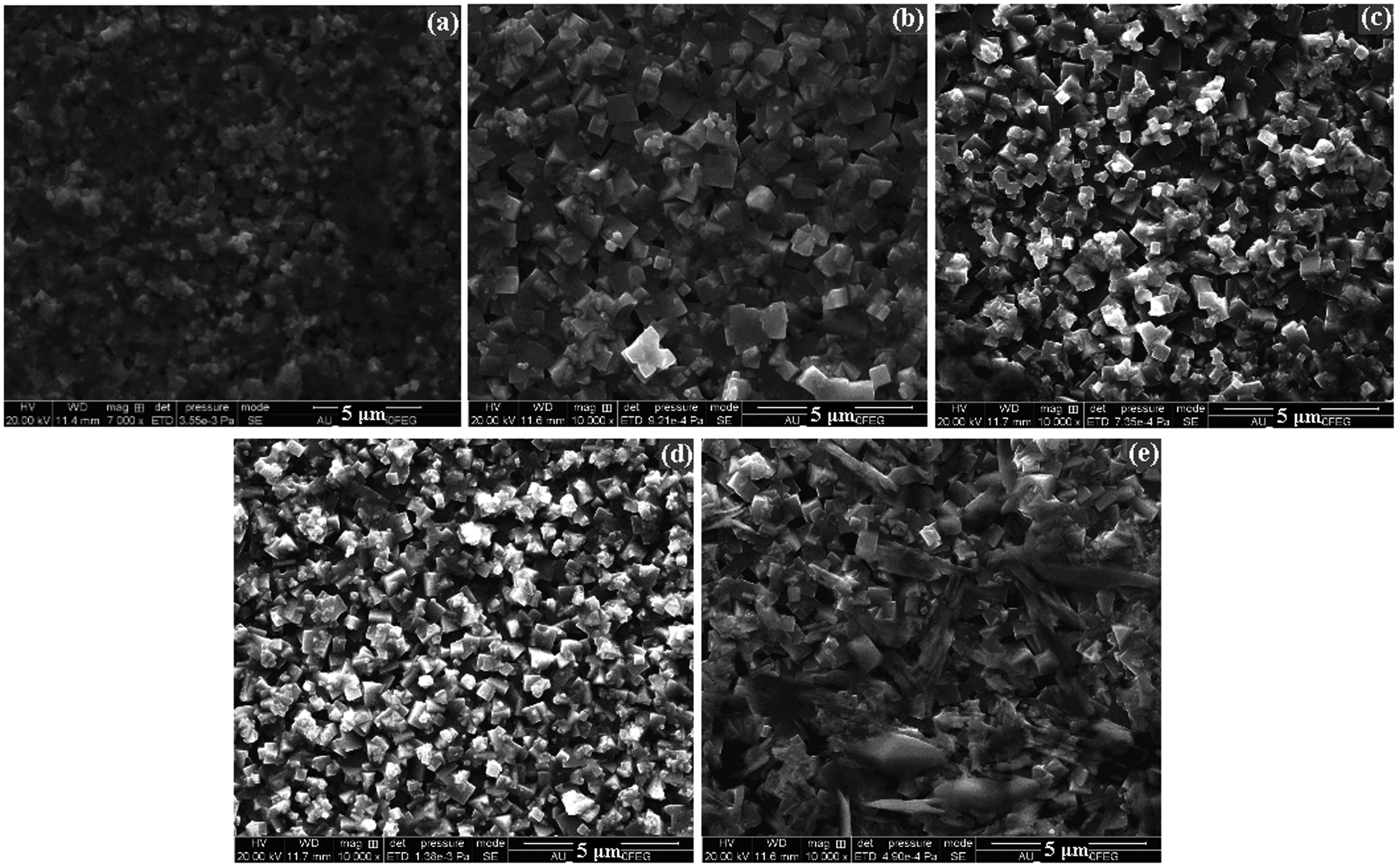
SEM images of PbS:Cd films coated with different Cd doping concentrations: a 0 at.-%, b 2 at.-%, c 4 at.-%, d 6 at.-% and e 8 at.-% Cd concentrations
Elemental analysis
Figure 3 shows the EDS spectra of PbS:Cd thin films coated with different Cd doping concentrations. The spectra confirm the presence of Cd in the doped samples. The atomic proportions of the elements Pb, S and Cd present in the films are shown in the insets.
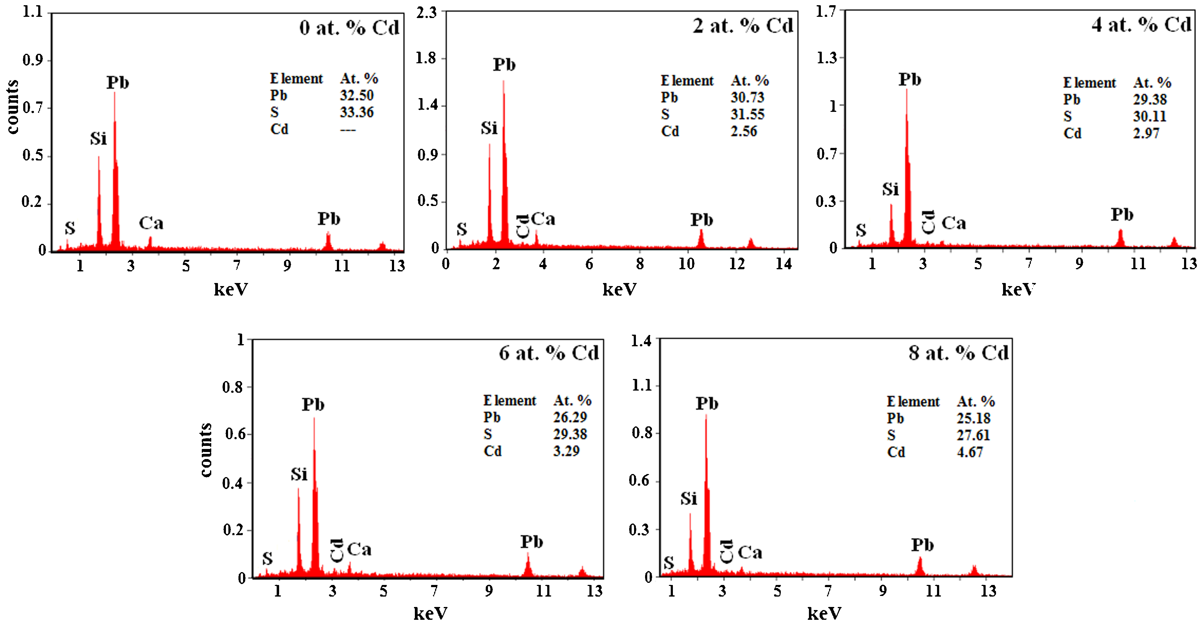
EDS spectra of PbS:Cd thin films
It can be seen that, as the doping concentration increases, atomic proportion of Cd increases, whereas Pb content decreases which very well supports for the successful substitution of Cd2+ ions in Pb sites. It can also be observed that as the doping concentration increases, S vacancies increases which improve the electrical conductivity of the doped films (the section on ‘Electrical properties’). It is evident that the S/(Pb+Cd) ratio of the PbS:Cd film deposited with 6 at.-% Cd dopant is approximately equal to 1, confirming its perfect stoichiometric nature and this might be the reason for its improved structural, morphological, optical and electrical properties.
Optical studies
The transmission spectra of the PbS:Cd thin films are shown in Fig. 4. As can be seen from Fig. 4, the overall film transparency increases with Cd doping concentration up to 6 at-% and then it decreases for further doping. A high transparency (∼77 %) is observed for the film coated with 6 at-%Cd dopant. The improved crystallinity of this film as evident from the structural studies might be the reason for its increased transparency. Due to the improved crystallinity, film roughness decreases which minimises light scattering inside the layer and hence, the transparency increases. The optical band gap (Eg) values are evaluated from the Tauc's plots (Fig. 5). The band gap value of undoped PbS film was found to be 1·96 eV, which exactly matches the value reported by Abbas et al. 25 for chemically deposited annealed PbS thin film. The variation of Eg as a function of Cd doping concentration is shown in the inset of Fig. 5. As seen from the inset fig, the band gap value increases with Cd doping concentration up to 6 at-% and then decreases for further doping. Such type of change in the band gap could be due to the structural modification, which takes place due to the replacement of either substitutional or interstitial lead ions in the PbS lattice by cadmium ions. Enhancement in the optical band gap with doping has been reported by others.26,27 It is well known that the properties of nanocrystalline materials change from their corresponding bulk properties, because the sizes of the crystallites become comparable to the Bohr excitonic radius. 28 In nanocrystalline materials, band bending effect can be expected at the grain boundaries as the surface to volume ratio is higher. In crystallites with smaller size, the band bending effect will be more compared to bigger crystallites. The increased crystallite size values observed for the films up to 6 at-% doping concentration (Table 1) leads to quantum confinement of the charge carriers in the crystallites and this result in the reduction of band bending effect. This might be the reason for the increased band gap values observed up to this doping concentration. 29 Owing to quantum size effect, the band gap increases due to reduced crystallite size, which result in the shift of absorption threshold to shorter wavelength due to individual confinement of electrons and holes. The converse result obtained here might be due to the excitonic confinement associated with larger crystallites. The energy gap broadening may also be related to the existence within the band gap of a high density levels with energies near the bands, which can give rise to band tailing, as has been suggested for other polycrystalline materials. The band gap values obtained for the PbS:Cd films are within the solar spectral region and hence these films find potential applications in solar cell fabrication.
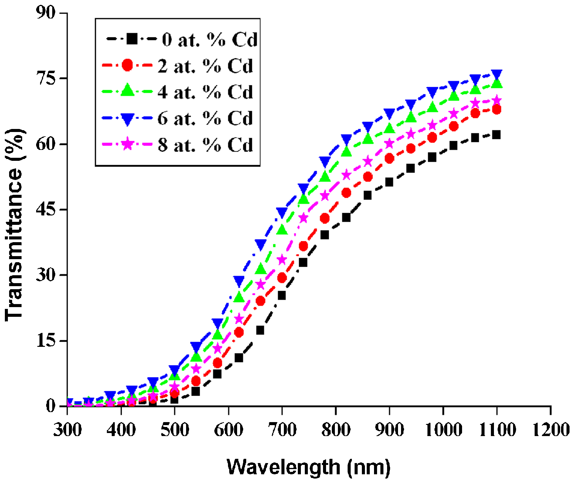
Transmission spectra of PbS:Cd thin films
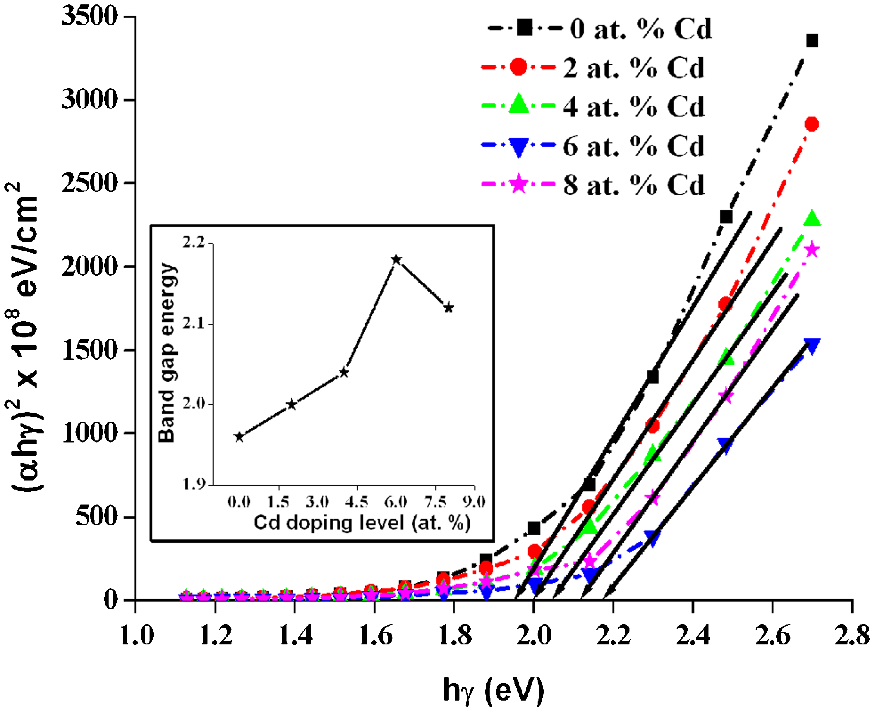
Variation of (αhγ)2 with hγ and band gap energy with Cd doping concentration (inset) of PbS:Cd films
Electrical properties
The electrical conductivity values of PbS:Cd thin films are given in Table 1. For undoped film, the conductivity is found to be 0·164×10−1 Ω cm−1. As the Cd concentration increases, the conductivity increases until it attains a maximum value of 12·67×10−1 Ω cm−1 for the film coated with 6 at-%Cd and for further increase in doping concentration it decreases. The conductivity values obtained here are in good agreement with the value obtained by Salim and Hamid 30 for chemically deposited PbS films. It is well known that in polycrystalline thin films, the electrical conductivity is strongly influenced by crystallite size and the characteristics of grain boundaries. The increased crystallite size and decreased strain values obtained for the doped films up to 6 at-%Cd concentration (Table 1) might have played a major role in the enhancement of their conductivity values. The increase in electrical conductivity might also be due interstitially or substitutionally placed Cd atoms which act as donor impurities. This is in accordance with the results obtained by Preetha and Ramadevi 13 for Al doped PbS thin films.
Conclusion
Good crystalline quality PbS:Cd thin films were deposited by spray pyrolysis technique with different cadmium doping concentrations. XRD studies revealed that all the films exhibited face centred cubic structure with a (2 0 0) plane preferential orientation. From the SEM images, it can be observed that Cd doping level largely governed the surface morphology of the PbS films. The band gap values obtained are within the solar spectral region which makes the PbS:Cd films a potential candidate in solar cell applications. Film coated with 6 at-%Cd dopant exhibits a maximum conductivity of 12·67×10−1 Ω cm−1. The structural, morphological, optical and electrical studies infer that the PbS:Cd film coated with 6 at-%Cd dopant concentration had better physical properties.
Footnotes
Acknowledgements
The authors are grateful to the Secretary and Correspondent, AVVM Sri Pushpam College (Autonomous), Poondi, India, for his excellent encouragement and support to carry out this work.