
Abstract
In this work, we report the electrochemical formation of Ta2O5 films with different morphology via one-step anodisation of tantalum foil in aqueous electrolytes consisting of H2SO4 and fluoride ion and small additions of ethylene glycol or glycerol. The morphology and structure were characterised by field emission scanning electron microscopy (SEM), X-ray diffraction and energy dispersive X-ray spectroscopy. SEM results show that under optimised electrochemical conditions in electrolytes containing H2SO4 and fluoride ion, Ta2O5 nanotube layers can be grown up to thickness of 2 μm. The addition of ethylene glycol or glycerol to this aqueous electrolyte resulted in the formation of irregular porous or compact films on the surface of tantalum. The photocatalytic activity of films was evaluated by measuring the degradation of methylene blue under UV irradiation. Ta2O5 nanotubes exhibited higher photocatalytic activity than did the other samples. The reason of this enhanced photocatalytic property can be attributed to high specific surface areas and the nanotube structures of this sample.
Introduction
There is significant interest in the fabrication of nanostructures such as nanoporous and nanotubular due to their wide applications. Nanostructures are of significant interest for the biomedical sciences, catalysis and chemistry, electronics and semiconductors, photonics, energy, and so on. Inorganic nanoporous structures, such as metal oxides, also have promise as components in solar cells, photocatalytic water splitting and electrolysis of water, fuel cells, molecular filtration and tissue engineering. Nanoporous metal oxide structures produced by the electrochemical anodising of some metals, such as aluminium, zirconium, titanium, tungsten, hafnium, niobium, iron and, recently, tantalum, have attracted additional interest because of their potential use in various areas of technology.1–7 All of these metals have been reported to form both disordered and ordered porous oxide structures by anodising method, except for tantalum, at which only disordered porous oxide layers can be formed.8–10 While compact Ta2O5 films are of high quality and have a well defined thickness that is directly proportional to the applied voltage, a key goal remains to be the fabrication of ordered Ta2O5 nanotubes. 11 Therefore, our focus in the present work is on the formation of organised, nanotubular oxides on tantalum by electrochemical anodising method. During the past 50 years, the anodic growth of tantalum oxide (Ta2O5) films has received considerable interest due to the film's specific properties such as its high dielectric strength or the bioinert behaviour that make it useful in various applications. 10 Although Ta2O5 is the most stable valve metal oxide against chemical dissolution in many environments, it can be dissolved in HF containing electrolytes forming soluble fluoro-complex. 10 The first reports of the formation of thick anodic Ta2O5 films, instead of the much more easily formed compact layers, showed that small amounts of HF added to H2SO4 solution produce a disordered, porous oxide layer.12–14 The fluoride ions are suggested to provide mild dissolution of the electrochemically generated oxide, which is continuously reformed in the presence of the high electric field. It is widely accepted that competition between oxide growth and dissolution leads to the continuous growth of porous oxide films. 10 Although several practical applications have been proposed for these porous Ta2O5 layers, their usefulness has been limited by their lack of order.12–14 Therefore, subsequent studies have focused on controlling oxide film morphology. In this regard, electrochemical formation of self-organised high aspect ratio Ta2O5 layers, by anodising of tantalum in non-aqueous electrolytes consisting of glycerol and small additions of NH4F, was reported by Wei et al. Under optimised conditions in these electrolytes, they were able to create Ta2O5 layers with thickness of 15 μm and pore diameter in the range of 10–40 nm. 10 Controlled formation of high aspect ratio Ta2O5 nanotubes by Ta anodising in H2SO4 + HF solutions was done by El-Sayed and Birss. 11 In addition, Allam et al. prepared high aspect ratio tantalum oxide nanotube arrays via one-step anodisation of Ta foil in aqueous electrolytes containing HF–H2SO4 with various volumetric ratios. 8 Another recent study showed that highly ordered and mechanically stable micrometer long Ta2O5 nanotube arrays can be fabricated by galvanostatic anodising in H2SO4 with additions of 13·6 wt-% H2O and 0·8 wt-% NH4F in a few seconds. 15 In this study, we report the fabrication of tantalum oxide films with different morphology by one-step anodisation of tantalum foils in electrolytes containing concentrated H2SO4 and fluoride ion with ethylene glycol or glycerol. Energy dispersive X-ray spectroscopy (EDX) and X-ray diffraction (XRD) were employed to get information on their structure and composition, while their morphology was studied by scanning electron microscopy (SEM). The photocatalytic activity of these films was evaluated by measuring the degradation of methylene blue (MB) under UV irradiation. Ta2O5 nanotubes showed higher photocatalytic activity than did the other structures.
Experimental
Ethylene glycol, glycerol, NH4F, HF, H2SO4 and HNO3 were of analytical grade. Other chemicals were obtained as analytical reagent grade and used without further purification. The solutions were prepared with distilled water. Tantalum (Ta) foils (purity >99·99%, 1 mm thickness) were used. MB (purity, 99%) was used as received. Its molecular formula is C16H18N3SCl (molecular weight, 319·85 g mol-1). MB is a cationic dye, used extensively for dying cotton, wool and silk. The risk of the existence of this dye in waste water has arisen from the burns effect of eye, nausea, vomiting and diarrhea. MB has a maximum absorption in the 660 nm visible area. 9
A piece of tantalum sheet was cut into desired dimension and was used as working electrode in the experiment. The working electrodes were sealed with insulation resin, leaving only desired active surface. Before the anodising, tantalum foil was cleaned by sonicating in acetone, isopropanol, ethanol, methanol and distilled water, and then dried in air. After cleaning, anodic films were grown from tantalum by anodising of tantalum foil in electrolytes containing concentrated H2SO4 and HF or NH4F and some additives such as ethylene glycol and glycerol. The anodising was performed using a two-electrode cell with tantalum foil as the working electrode and platinum foil with ∼14 cm 2 area as the counter electrode, under constant applied voltage at room temperature (∼25°C). A controlled DC power source (ADAK, PS405) supplied the required constant voltage, and a digital multimeter (Senit, DT-9208A) measured the anodisation current. After anodising, the as formed samples were annealed in oxygen atmosphere at 400°C for 2 h with a ramp of 5°C min− 1 to obtain crystalline samples. In the present work, we compare the photocatalytic performance of tantalum oxide films with different morphology referred to as A, B and C. Table 1 summarises the experimental conditions for three different samples.
Experimental parameters for fabrication of different films
The surface morphology of all samples was characterised by field emission SEM (FE-SEM, Hitachi S-4160, Japan), and the elemental composition was estimated by EDX. Elemental mapping was conducted by energy dispersive spectroscopy. The crystalline phases were identified by XRD with Equinox 3000 diffractometer (Inel, France). Diffraction patterns were recorded in the 2θ range from 20 to 80° at room temperature.
Photocatalytic activity of all the samples was evaluated by degradation of the aqueous MB under UV light irradiation. The photocatalytic reaction was carried in a single compartment cylindrical quartz reactor. A 400 W high pressure Hg lamp was used as a light source. The luminous intensity of this lamp was 200 mW cm− 2. One hundred per cent of the light was transmitted by the quartz glass as lamp shone on the samples. A fan was used to cool down the reactor tube. The actual experiments were performed at room temperature. The initial concentration of MB was 2 mg L− 1. The volume of the solution was 50 mL. Before illumination, the photocatalyst sample was immersed in quartz reactor containing MB and magnetically stirred for 2 h in the dark to ensure the establishment of an adsorption–desorption equilibrium between the photocatalyst and MB. Then, the solution was exposed to UV irradiation under magnetic stirring for 2 h. At each 10 min intervals, 5 mL solution was sampled and the absorbance of MB was measured by a UV–Vis spectrophotometer to determine the extent of degradation.
Results and discussion
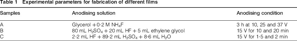
The morphology of samples anodised in different electrolytes was observed by SEM. Figure 1 shows FE-SEM images of A, B and C respectively, which clearly shows formation of films on the surface of tantalum. Figure 1a shows SEM images of anodic oxide layers grown on tantalum by anodisation in glycerol with 0·2 M NH4F under voltages of 10 V (a1), 25 V (a2) and 37 V (a3) for 3 h. From the SEM images, it is evident that an irregular porous film formed on the surface of tantalum, and by changing the voltage, their morphology will change. The formation of such porous structures has been reported in other metals. Most recently, first reports appeared that show self-ordered formation of porous nanostructures with a through hole morphology on titanium, niobium and some alloys in organic electrolytes containing
SEM top view images of Ta2O5 films with different magnification: a sample A; b sample B; c sample C .16,17 Another case of creating ordered porous structures of TiO2 formed by anodisation is so called non-thickness limited oxide formed in hot glycerol phosphate electrolyte.18,19
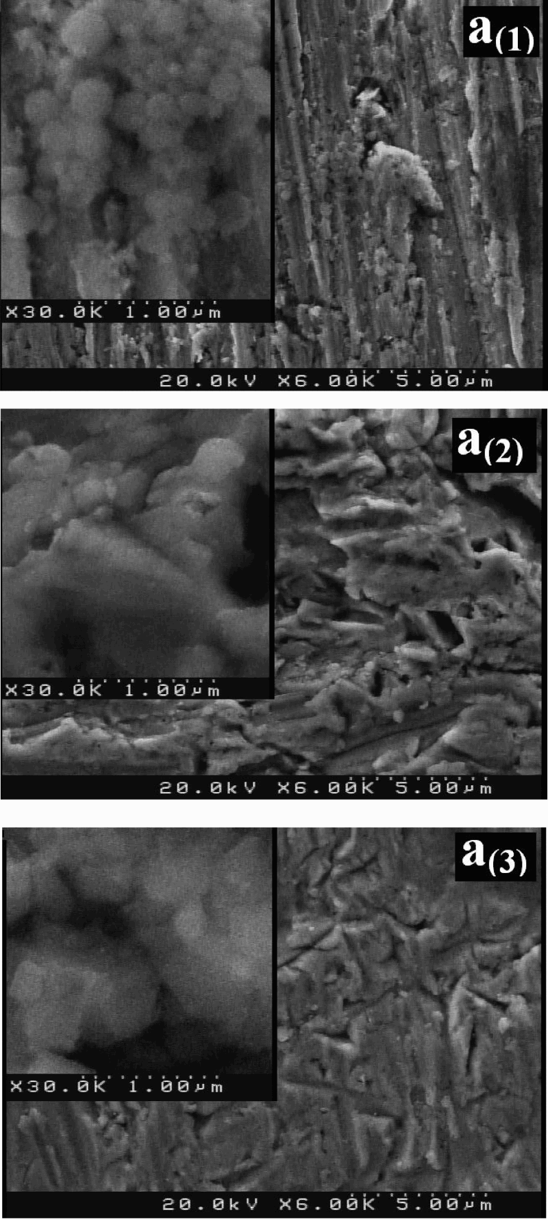
Figure 1b shows an illustrative FE-SEM image of tantalum surfaces anodised at 15 V for 10 min (b1) and 20 min (b2) in an electrolyte containing concentrated HF and H2SO4 in the volumetric ratio 2:8 in the presence of 5 vol.-% of ethylene glycol. Images show that a compact film, without porosity, was formed on the surface of tantalum. Ta2O5 film by anodising for 10 min contains irregular cracks (b1), and anodising for 20 min creates film contains grooves (channels) that are parallel to each other (b2). Under certain circumstances, compact films can be created on other metals. In general, a compact layer of an anodic oxide can be formed in electrolytes in which a very low solubility of the oxide in the electrolyte is provided. It must be noted that most metals are covered with an ultrathin air formed oxide. The structure of this air formed oxide differs from that formed by anodising and is considered to have an impact on the formation of the latter one. Wu et al. have prepared compact layer of TiO2 on the surface of titanium alloys by anodisation in an aqueous solution of 0·2 M sodium tartrate. 20 Other studies have shown that in most cases, anodising of titanium in alkaline solution leads to the formation of compact films on the surface. 21
Figure 1c describes the top morphology of tantalum oxide nanotube array films, which were obtained by anodising of tantalum under 15 V for 90 s in an electrolyte containing HF (2·2 mL), H2SO4 (89·2 mL) and distilled water (8·6 mL). The highly ordered tantalum oxide nanotube arrays clearly have been formed on the surface of the tantalum substrates, and these nanotubes are parallel to each other and perpendicular to the substrate. Unlike the tantalum, titanium oxide nanotubes formed by anodising have been widely studied. 21 In most cases, TiO2 nanotubes formed in fluoride electrolytes. The first self-organised anodic oxides in the form of pores were formed on Ti by Zwilling et al. in 1999 using dilute fluoride containing electrolytes. 22 Titanium oxide nanotubes formed in aqueous electrolytes and their geometry could strongly be improved by modification of the electrolyte composition and its pH. One of the most crucial changes in improving the nanotube morphology was the introduction of organic electrolytes. 23 By anodising of titanium in organic electrolytes such as dimethyl sulphoxide, glycerol or ethylene glycol with small content of water and fluoride ions, TiO2 nanotubes of a very uniform shape were formed. 21 These nanotubes were much more organised, and they could be grown to hundreds of micrometers in length.21,23
In general, anodising of valve metals leads either to the formation of compact oxide layers (barrier type anodic oxides) or porous oxides in the form of nanopores, nanotubes (ordered or disordered layers) and fishbone structures, mainly depending on the used electrolyte. Similar to tantalum, various morphologies of titanium anodic oxides were produced and studied. Recently, Kowalski et al. have reviewed recent advances in the formation of nanostructured oxides in the form of nanotubes, nanopores, mesosponges, nanochannels and microcones grown on Ti, Nb, Ta, Zr, Hf, W, V and their alloys; discussed mechanisms of their formation and key functional features; and described their applications in various fields of chemistry and electrochemistry. 23
From the cross-sectional view of tantalum oxide nanotube arrays in Fig. 2, it can be seen that the formed nanotubes are parallel aligned; the external diameter and the length of the nanotubes were measured to be ∼55 nm and ∼2 μm respectively. The cross-section view in Fig. 2b shows that the thickness of this nanoporous Ta2O5 layer is uniform. Based on the SEM results, it can be said that the morphology of Ta2O5 layers can be modified by the electrochemical conditions (potential, electrolyte and time) and Ta2O5 nanotube layers can be formed by anodising of tantalum in optimum electrolyte composed of HF and H2SO4.
Cross-sectional image of Ta2O5 nanotubes (sample C); XRD patterns of Ta2O5 nanotubes: a as prepared; b annealed at 400°C
XRD analysis is a useful technique that can be used to identify the crystalline structure of samples. The XRD patterns of Ta2O5 film are shown in Fig. 2. As displayed in the figure, the as prepared film was amorphous because no discernible diffraction peaks were observed in its XRD pattern besides the diffraction peaks of tantalum substrate. However, for the sample obtained after annealing in oxygen atmosphere at 400°C for 2 h with a ramp of 5°C min− 1, the appearance of some new diffraction peaks was indicative of the formation of Ta2O5.
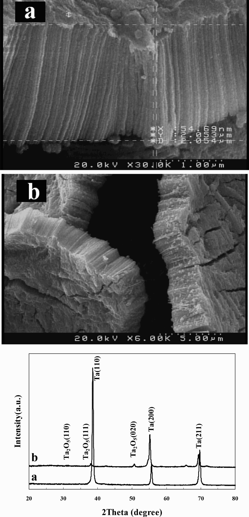
The elemental compositions of the as prepared tantalum oxide nanotube array film were studied by EDX and energy dispersive X-ray mapping, and the results are displayed in Fig. 3. The data confirm that the samples are composed of Ta and O. The occurrence of traces of contaminants such as the fluorine and sulphur from precursors is also observed. The elemental maps demonstrated that O and Ta are homogeneously distributed on the surface of sample.
EDX spectra and EDX mapping of Ta2O5 nanotube samples indicating spatial distribution of different components on surface of this sample
The presence of fluorine and sulphur indicated that these elements were doped in tantalum oxide films. In semiconductor production, doping intentionally introduces impurities into an extremely pure semiconductor to change its electrical properties. 24 A dopant (doping agent) is a trace impurity element that is inserted into a substance (in very low concentrations) in order to alter the electrical properties or the optical properties of the substance. There are different methods to doping the semiconductors. 24 One of the methods for doping elements is in situ doping. In situ doping is a process that dopant is added during deposition. In this method, dopant atoms are introduced into the semiconductor during its growth.2,24 A direct one-step facile approach for the in situ doping of titania and alumina is adding the desired element (in the form of its salts) in the anodising electrolyte.25–30 The significance of these layers is one step and easy synthesis of them, achieving the optimal morphology of films by controlling various parameters of anodising such as anodising voltage, time, electrolyte temperature, electrolyte type and concentration. In addition, in these layers, different amounts of desired dopants were doped during synthesis of these films and this reduces the cost of prepared material.
Figure 4A shows the current density–time curves recorded during anodising of tantalum at the different electrolytes (samples A–C). Typically, the current densities decrease gradually in the initial period, and then slowly reach a steady value, which is voltage dependent. Similar to titanium, initially, a compact oxide layer is formed through hydrolysis of tantalum.8,10 This oxide layer leads to a dramatic decrease in the anodisation current due to its poor electrical conductivity. Note that the current decreased drastically in a few seconds from an initial value of ∼2 to ∼0·3 mA in ethylene glycol containing electrolyte, ∼0·4 mA in glycerol containing electrolyte and ∼0·1 mA in electrolyte containing HF, H2SO4 and water. The thickness of anodic oxide films formed on metals such as aluminium and titanium has been argued previously to be controlled by a balance between the rate of electrochemical formation of the oxide film at the underlying metal surface and the rate of oxide dissolution, as shown in reactions (1) and (2) respectively for tantalum in these solutions8–10:


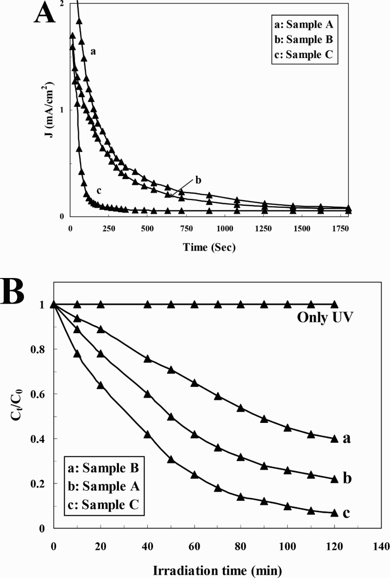
A Current transient curves recorded during anodising of tantalum in different electrolytes; a, sample A; b, sample B; c, sample C; B photocatalytic degradation of MB over different samples under UV irradiation
Photocatalytic activity of different samples was followed through degradation of MB as a function of irradiation time with UV irradiation. The time dependent degradation of MB solution in the presence of both light and Ta2O5 films is shown in Fig. 4B, from which a gradual decrease in the absorption of MB is observed. Appearance of no new absorption peak during the whole process indicates the complete photodegradation of MB. No degradation of the dye was observed in the presence of only light. In addition, a dark control experiment was conducted, indicating that the adsorption of MB onto the surface of the catalyst in the absence of UV irradiation was negligible. The photocatalysis results indicated that the photocatalytic process was very effective in the removal of MB, and it was observed that tantalum oxide nanotube films (sample C) exhibit higher photocatalytic activity for MB degradation compared with the two other Ta2O5 films (samples A and B). The improved photocatalytic activity of this sample can be explained by the high specific surface areas and the nanotube structures. The large surface area can offer more adsorption sites and photocatalytic reaction centres. The nanotube structure can enhance the adsorption efficiency of light and the diffusion rates of reactants and products.
Conclusion
In summary, various structures of Ta2O5 films were fabricated via anodisation of tantalum in aqueous electrolytes containing HF and H2SO4 along with low concentrations of ethylene glycol or glycerol. Results showed that the morphology of Ta2O5 films depends on the applied potential as well as the electrolyte composition. The best results in terms of homogeneity, ordering and aspect ratio were achieved in electrolytes containing H2SO4 and fluoride ion at the applied voltage of 15 V having an external diameter of 55 nm and a thickness of 2 μm. Owing to high surface/volume ratio of Ta2O5 nanotubes, these layers are candidate materials for different applications and exhibited a higher photodegradation activity of MB compared to other films.