
Abstract
Pulse electrodeposition method is employed for the synthesis of Sn nanostructures using alumina template. Electrical contacts are made through metallisation of the template bottom with copper and an aluminium foil. The current density is varied from 0.05 to 0.6 A cm− 2, and a change in nanostructure formation is noticed. The structure and morphology of nanostructures are characterised by X-ray diffraction, field emission scanning electron microscopy and energy dispersive X-ray spectroscopy. It is observed that at a lower current density (0.05 A cm− 2), nanorods (mean diameter 186 nm) are prominent. As the current density is further increased to 0.4 A cm− 2, the nanorods increase in diameter (∼216 nm), while at a higher current density of 0.6 A cm− 2, nanorods (mean diameter 158), nanoribbons (mean diameter 126 nm) as well as nanowires (∼44 nm) are produced. The obtained Sn nanostructures are polycrystalline in nature and can be scaled up to industrial level.
Introduction
Tin is the choice of material in advanced microelectronics packaging.1–4 Nowadays, Sn nanowires are the centre of attraction among researchers on account of their interesting properties compared with the same material in the bulk state. Interests in nanostructure formation are generated because of their unique properties in the field of electronics, catalysis, sensors, electrodes for batteries, etc.5–8 There are various routes for the fabrication of one-dimensional nanostructures in the literature, for example, bottom up approaches like sonochemical method, atomic layer deposition, ion beam lithography, template assisted electrochemical deposition, etc. Top down techniques are also available, for example, electron beam evaporation, chemical vapour deposition and physical vapour deposition.9,10 Most of these evaporation processes, where the atoms are sputtered over the membrane (substrate), may cause gradual accumulation of materials at the top, leading to the blockage of membrane pores or channels. This may result in wastage of material and poor efficiency.
A reasonable and complete filling of the template channels is mainly achieved by a bottom up approach. Thus, among the other methods, a bottom up approach like electrodeposition is a convenient method to ensure a direct and complete filling of the channels or pores.11,12 The electrochemical deposition process is promising in this regard because of its significant advantages, such as simplicity, economical and ability to produce high aspect ratio nanostructures. 12
However, in electrodeposition, the morphology of a coating depends on various factors, such as current density, temperature, pH and additives.13,14 Pulse electrodeposition has already been applied to generate a wide variety of nanostructured materials, including Sn based nanocomposites.15,16 The most important variable in electrodeposition is current density, which is supplied to the cathode. An enormous amount of research activities has been carried out in the past on the influence of current density to control the morphology of the deposits.17–20 The fabrication of Sn nanostructures by pulse electrodeposition using an anodic aluminium oxide membrane is currently the most attractive technology to grow Sn based nanostructures and nanotubes due to the high degree of control and precision on the nanostructures obtained. 10 However, the template assisted method has an inherited drawback to not control the inside diameters of nanostructures. There are various applications where precise control of the diameter is demanding.21,22 Therefore, influence of deposition parameters on the template assisted electrodeposition method for the design and synthesis of Sn nanostructure arrays is required. This work is concerned with studying the effect of varying current density during pulse electrodeposition to understand the growth morphology and pattern of the nanostructures produced.
Experimental
Template preparation
Commercial anodic alumina membranes (anodic aluminium oxide anodiscs made by Whatman, Sigma Aldrich) having an average pore diameter of ∼200 nm are used as templates. The template is washed with distilled water to remove any adherent impurities like dust or other inclusions. Later, the template is washed in ethyl alcohol in order to remove any oily or greasy medium that may have accumulated on the surface of the template followed by drying in air.
Substrate preparation
The as prepared template is coated with a conductive layer of Au–Pd alloy (∼200 nm) on the bottom side of the template using a conventional sputter coater to facilitate the conductivity of the surface. After that, ∼500 nm layer of copper is also sputtered (using radio frequency/direct current magnetron sputtering system, KVL Ltd) over the channels of the alumina template. The copper acts as a seed layer to facilitate the cathodic electrodeposition of Sn.
Now, an aluminium foil with a thickness of 10 mm is utilised for providing the electrical contacts to the membrane through a conducting paste over the copper coated side. Since the electrodeposition process needs an electrolytic contact of the active metal surface, a small area of the aluminium support (in the order of 0.25 cm2) is exposed to the plating bath.
Electrolytic bath preparation
The electrolyte is prepared for the electrodeposition process by adding the following chemicals:
SnCl2.2H2O (50 g L− 1) Tri-ammonium citrate (100 g L− 1)
All the chemicals are procured from Merck, with 99.8% purity and of electrolytic grades. The tri-ammonium citrate acts as a stabiliser that helps to dissolve SnCl2.2H2O (which is sparingly insoluble in water) and thus stabilise the plating bath. 19 Triton X-100 (∼0.1 g L− 1) is also added as an additive to provide uniform deposition throughout the template pores. It is noteworthy that the main role of an additive is to relieve the internal stresses in the electrodeposited nanostructures.13,14 The bath pH is measured using a Systronics digital pH meter 802 and is found at ∼4.3. There is no appreciable change in the bath pH during electrodeposition. The bath temperature is continuously monitored at room temperature (∼28°C) using an electronic thermometer. The solution is continuously kept on stirring at 300 rev min− 1 during electrodeposition by a Tarsons made SPINOT magnetic stirrer.
Pulse electrodeposition
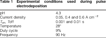
The electrodeposition of the Sn nanostructures is carried out using an Autolab PGSTAT 32 (Metrohm, Netherlands) with a 10 A current booster. The electrochemical cell consists of a three-electrode geometry. The pure tin slab (Merck, 99.8%) is used as anode for deposition, and the Cu metallised alumina substrate is used as cathode. An Ag/AgCl (1M KCl) standard electrode is used for the measurement of the reference time–voltage during the electrodeposition experiment. A schematic diagram of the arrangement used for the fabrication of Sn nanostructures is shown in Fig. 1. The deposition is carried out under varying values of current densities, that is, (1) 0.05 A cm− 2, (2) 0.4 A cm− 2 and (3) 0.6 A cm− 2. For each case, the electrodeposition is carried out for 3 h, with pulse on time (Ton) and pulse off time (Toff) values being set at 0.001 and 0.01 s with a frequency of 90 Hz. A typical waveform used for the pulse electrodeposition is shown in Fig. 2, and the electrical parameters are summarised in Table 1.
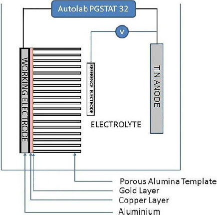
Schematic illustration of template assisted pulse electrodeposition
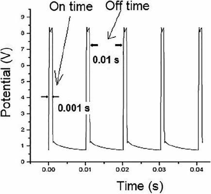
Typical pulse current waveform used for pulse electrodeposition of Sn nanostructures
Experimental conditions used during pulse electrodeposition
Recovery of nanostructures
After the pulse electrodeposition experiment, the template is taken out from the plating bath carefully and washed with distilled water followed by ethanol. The washed template is then completely immersed in 4 M NaOH solution. As a consequence, the template is preferentially dissolved away in this fashion, and the fabricated free standing nanostructures get separated out.
Characterisation details
Phase structure
The X-ray diffraction (XRD) experiments are carried out using an X-ray diffractometer (Bruker's D8 Advance) with co-target operating at 40 kV and 30 mA. The various phases formed during deposition are identified by comparison of the recorded diffraction peaks with the Joint Committee on Powder Diffraction Standards (JCPDS) database embedded in a Philips X'Pert HighScore Plus software.
Growth morphology of nanostructures
The structure and distribution of Sn nanostructures in the template are examined using field emission scanning electron microscopy (FESEM) (Carl Zeiss Supra EVO 60). The compositional analysis is performed with energy dispersive X-ray spectrometer (EDS) attached with the FESEM.
Results and discussion
Phase structure
The Sn nanostructures are characterised for their presence by an XRD study. The XRD pattern obtained is shown in Fig. 3a. The diffraction pattern is analysed using JCPDS data card number 04-0673, as shown in Fig. 3b. The position of the reflection peak with the highest intensity is found to be at 35.791°, which corresponds to the (200) plane of the tetragonal (β-Sn) lattice. Two other minor β-Sn peaks are also noticed at 65.257 and 75.766°, which match the (301) and (400) planes of the β-Sn lattice respectively. There is no other peak detected in the spectrum. The XRD measurements thus confirm that the nanostructures formed are of tetragonal (β-Sn) structure only. There is no contamination from the aluminium support or copper metallisation, confirming the purity of the nanostructures.
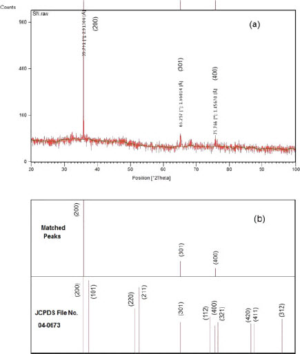
a X-ray diffraction pattern of Sn nanostructure obtained (current density is 0.6 A cm− 2) and b comparison of XRD pattern with standard JCPDS data
Compositional analysis
Figure 4 shows the EDS compositional analysis of the template deposited Sn nanostructures with and without templates. It is observed from Fig. 4a that different elements, i.e. oxygen, aluminium, tin and copper, are present in the sample with template unetched. The presence of oxygen and aluminium is expected from the anodic alumina template, while the tin is from the deposited nanostructures. Copper is also detected from the seed layer of the template metallised before the deposition. It is also observed that after recovering the nanostructures from the templates, there is no trace of the elements from either metallised layer Cu or the aluminium contacts (Fig. 4b). Various peaks corresponding to only tin are present, showing the high purity of the nanostructures obtained.
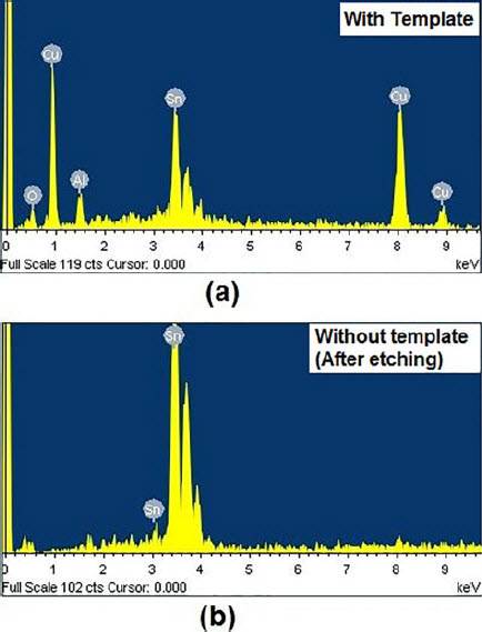
Energy dispersive X-ray spectrum of samples: a alumina template filled with Sn nanostructures (without etching); b Sn nanostructures after etching of alumina template with 4M NaOH solution (current density is 0.6 A cm− 2)
Nanostructure morphology
It is observed that when the current density is varied, a Sn nanostructure is formed with different sizes and shapes. This section describes the surface morphology of Sn nanostructures formed at various current densities.
Case 1: 0.05 A cm−2
The following images show the morphologies of the nanostructures electrodeposited at a very low current density of 0.05 A cm− 2 (Fig. 5). At a low resolution (Fig. 5a), free standing nanorods are visible, which are properly aligned in the vertical direction. The top surface of the template is shown in Fig. 5b, where incomplete filling of the channel/pores is also noticed. The filled in pores of the template are shown by encircled regions. It is clearly evident that most of the pores of the template remain unutilised. It is observed that the nanorods are not present in all the pores of the template, and only a few channels are occupied with the tin nanorods successfully. The cross-section is also analysed at higher resolution, and it is observed that these nanorods are formed with an average diameter of 186 nm. The size distribution of nanorods lies in the range of 146 to 240 nm. The length of the nanorods is short, i.e. 2 to 3 μm (Fig. 5c and d). A poor filling of template pores in this case may be due to the very low current density. A low current density causes lesser deposition efficiency, and hence some template pores are empty or half filled.
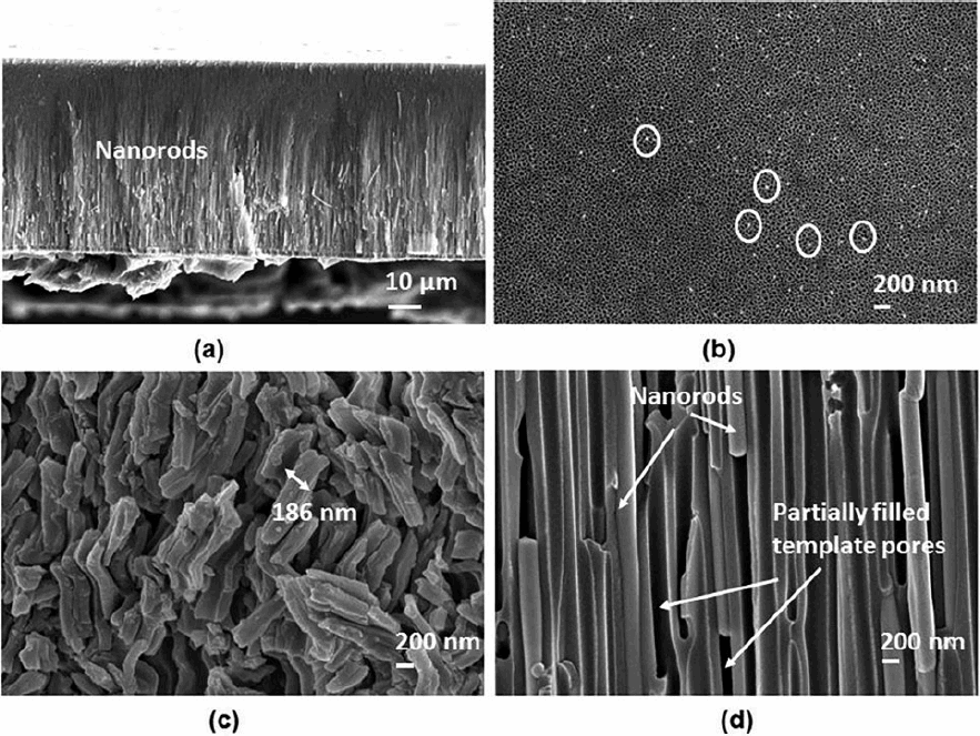
Image (FESEM) of nanorods obtained at current density 0.05 A cm− 2: a cross-section of template showing nanorods; b top view of template with nanorods; c high resolution image of nanorods taken from a; d cross-section view of template showing filling pattern of nanorods inside template pores
Current density: 0.4 A cm−2
Figure 6a shows that well aligned and fully grown nanorods are grown and found to be longer in length of 5 to 8 μm. In addition, the efficiency of the deposition process is much improved in this case as more Sn has been deposited and higher number of pores in the template are filled. This is confirmed from the top view of the membrane (Fig. 6b), where the filling of the pores is increased, as shown by the encircled regions. The white patches represent the places where the deposition has taken place, while the black spots are the pores that have not been filled.
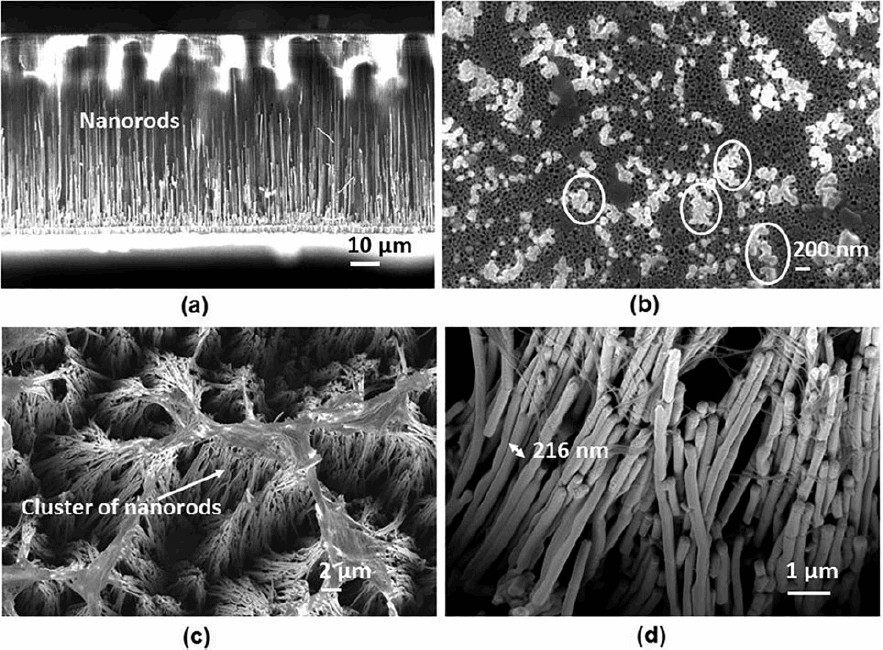
Image (FESEM) of nanorods obtained at current density 0.4 A cm− 2: a cross-section of template showing nanorods; b top view of template with nanorods; c high resolution image of nanorods taken from a; d cross-section view of template showing cluster of well developed nanorods
It is observed that the number density of the nanorod clusters increases appreciably with increasing the current density (Fig. 6c). It is also noticed that the nanorods have a larger average diameter 216 nm with a size distribution of 209 to 253 nm (Fig. 6d). This can be due to the fact that on increasing the current density during the deposition process, the nucleation sites in the pores increases, and therefore, the growth rate of the nanostructures become prominent.17–20
Current density: 0.6 A cm−2
Figure 7 shows that a number of nanostructures are obtained at a sufficiently high current density (0.6 A cm− 2). At low resolution, only nanorods are visible with a highest number density in this case (Fig. 7a). A top view of the membrane (Fig. 7b) demonstrates that the maximum coverage of pores has been achieved at this current density of 0.6 A cm− 2 due to the rapid deposition rate inside the pores. As a result, tin is deposited in most of the available template pores, as indicated in Fig. 7b. However, the dimensional stability of nanostructures is lost, and the nanostructures start to grow haphazardly in random directions (Fig. 7c). As a result, a mixture of nanowires and large diameter nanorods are observed. The mean diameter of the nanorods is 158 nm, while the nanowires are 2 μm long and 40 nm wide (with an aspect ratio of ∼50). A careful inspection of the high resolution image of the nanostructures (Fig. 7d) indicates the presence of a few nanoribbons along with the nanowires, which are 129 nm in diameter. This may be attributed to the fact that as the density of the nanowires is increased, they may adsorbed each other on their surface to form a ribbon shaped structure in due course of time (Fig. 7d). The nanowires are reported to form due to the “tip effect,” leading to a very high current density at the top of the Sn nuclei. 21 This localised current density triggers the formation of needle type growth, leading to the formation of nanowires. Generally, in the electrodeposition process, an unstable growth front can be attributed to the fact that when the current density is increased to a very high value, due to greater electron transfer rate concentration, polarisation increases associated with vigorous hydrogen evolution. This causes non-uniform growth of the electrodeposits. 14 However, the fundamental mechanism of the morphology of the unstable growth of nanostructures is not clear in the literature due to the complex nature of the pulse electrodeposition process. The pulse electrodeposition depends on several conditions and parameters, such as current density, temperature, bath pH, solution conductivity, quality of template, etc.14,23,24
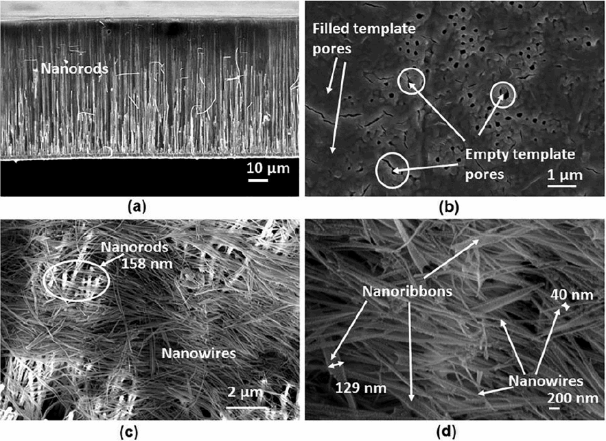
Image (FESEM) of nanorods obtained at current density 0.6 A cm− 2: a cross-section of template showing nanorods; b top view of template with nanorods; c high resolution image of cross-section of template showing cluster of nanorods, nanoribbons and nanowires; d cross-section view of template showing nanowires in c
The growth mechanism of nanostructures in template assisted electrodeposition can be explained as follows. The growth of nanowires under diffusion limited conditions will be independent of process parameters inside the template. In other words, when the current density is lower, diffusion is very slow. As the current density increases, the rate of diffusion increases due to the availability of a higher number of ions getting reduced in the template, thus enhancing the growth of incompletely formed nanowires at the cost of previously formed longer nanowires. This type of current gradient results in a uniform growth kinetics of nanowires. Various types of gradients have been used in the past for controlling interfacial instabilities.25–27 However, when the current density reaches a very high value, in the present investigation (i.e. 0.6 A cm− 2), the diffusion of electrolytes into pores increases at a higher rate. The inherent hydrogen evolution in the electrolyte becomes rapid at this stage, and the modification of inner shapes of nanostructures can be explained by the screening effect of hydrogen bubbles that screen the bottom surface of the pores. 29 Thus, the deposition gets confined within the gap between hydrogen bubbles and pore wall, and an unstable growth of nanostructures, non-uniform needle type or irregular growth may arise.28–29 As a consequence of this phenomenon, different shapes of nanostructures are observed, like nanowires and nanoribbons in the template. Therefore, it can be inferred that the current density can be an important parameter to monitor and produce various types of nanostructures using template electrodeposition.
Conclusion
Synthesis of various tin nanostructures is successfully carried out in the alumina template using the pulse electrodeposition technique. It is found that the synthesis of the nanostructures is deeply affected by the variation in current densities during the electrodeposition process. At low current densities of 0.05 A cm− 2, better alignment of the nanorods is obtained with short length (2 to 3 μm, dia 186 nm), while at 0.4 A cm− 2, the growth rate increases (5 to 8 μm length, diameter 216 nm). At a very high current density of 0.6 A cm− 2, nanorods, nanowires and nanoribbons are observed. The nanorods are formed with an average diameter of 158 nm. The nanowires are formed due to the dendritic growth of Sn inside the pores of diameter 40 nm with a very high aspect ratio of 50. Nanoribbons are also observed, which are believed to emerge from the joining of the various nanowires together with an average diameter of 126 nm. The mechanism behind the formation of nanostructures can be understood in detail with some more studies.