
Abstract
Thin films of titania (TiO2) doped with 1–5 wt-%Fe were spin coated on glass slides and then annealed at 500°C for 2 h. Results revealed that all of the films were ∼500 nm in thickness and consisted of anatase. Increasing the dopant levels revealed the following trends: the major (101) anatase peak shifted to larger lattice spacing [the peaks were normalised using the principal (210) chromium coating peak as an in situ standard]; the microstructures showed increasing shrinkage cracking, a phenomenon that has not been reported previously; the optical transmittance generally decreased; the amplitude of the transmittance curves generally decreased; and the optical indirect band gap decreased from 3·40 to 3·18 eV, possibly due to silicon contamination, residual thermal stress and/or the formation of midgap states from Fe doping.
Keywords
Introduction
Presently, titanium dioxide (titania) thin films are important materials for applications in dye sensitised solar cells1, 2 and photovoltaic cells3, 4 owing to their advantages, such as long term stability against photochemical corrosion, energy band edges that are well matched with the redox level of water, electronic properties that can be varied by changing the lattice defect chemistry or the oxygen stoichiometry and minimal or zero environmental impact. It is well known that TiO2 (anatase) can absorb light below the wavelength of 387·5 nm, producing a band gap of 3·20 eV; thus, it absorbs very little visible light (400–800 nm).5 Consequently, one of the key technological issues with regard to titania is the extension of the absorption region into the visible light range.
One of the most commonly used methods to enhance visible light absorption is to dope the material with cations and anions, including vanadium,6 chromium,7 iron,8 cobalt,9 copper,10 zinc,11 nitrogen12 and boron.13 Of the preceding, Fe is of interest owing to its octahedral trivalent radius of 0·079 nm, which is similar to that of octahedral tetravalent Ti (0·075 nm).14 Therefore, it can be inferred that Fe ions may be incorporated in the Ti sublattice in TiO2, and this would enhance oxygen vacancy formation, leading to an improvement in the photocatalytic performance of TiO2.15 However, it should be noted that, while doping with transition metals is an attractive method, it can also lower the crystallinity of the films.16
There are several methods to prepare Fe doped TiO2 films, including sputtering,17 pulsed laser deposition,18 metal organic chemical vapour deposition,19 anodic oxidation,20 dip coating,21 hydrothermal growth,8 electrohydrodynamic atomisation,22 ultrasonic spray pyrolysis23 and spin coating.24
The first three techniques in the preceding paragraph require a vacuum system to undertake the deposition, and this implies higher infrastructural costs; the latter three techniques are less suitable for large scale implementation. Moreover, the ultrasonic spray pyrolysis technique has a very low yield rate (∼5%).23 However, the advantages of spin coating over the other methods is its effectiveness, versatility and practicality with regard to the preparation of TiO2 thin films, and furthermore, the process can be carried out in atmospheric conditions, thus eliminating the need for a vacuum chamber and additional systems. The properties of the film depend only on three parameters, which are the spinning speed, solution concentration and annealing temperature. It is commonly known that high spinning speeds (⩾5000 rev min−1) will produce ultrathin films (<200 nm).25 On the other hand, thick films (about 1–2 μm) can be obtained using low spinning speeds (∼1000 rev min−1).25 Furthermore, with increasing solution concentration, the film thickness increases linearly. In the previous study by the authors,26 the annealing temperature was shown to cause both grain growth and phase transformation of anatase→rutile.
In the present work, Fe doped TiO2 films were prepared on soda lime silica glass slides using spin coating with a view to investigate the effects of the dopant concentration on the structural, morphological and optical properties of the thin films. An important aspect of this work is the use of a chromium coating, which was carried out as part of the sample preparation for analysis using scanning electron microscopy (SEM). This coating was found to be an essential step since it could be used as an in situ normalisation standard for critical data interpretation of the X-ray diffraction results.
Experimental
Solution precursors were prepared using titanium isopropoxide (TIP, reagent grade, 97 wt-%, Sigma-Aldrich) mixed with 10 mL of 12M HCl, followed by dissolution in isopropanol (reagent plus ⩾99 wt-%, Sigma-Aldrich) at a titanium concentration of 0·1M (2·8 g of TIP diluted to 100 mL volume with isopropanol); the solutions were mixed by stirring in glass at 400 rev min−1 for 15 min without heating. The Fe dopant concentration was varied in proportions of 1, 3 and 5 wt-%Fe (metal basis in TIP) by adding iron chloride tetrahydrate (FeCl2.4H2O, reagent grade ⩾98 wt-%, Sigma-Aldrich) to the solution. Spin coating (Laurell WS-65052) was carried out by dropping ∼0·2 mL of solution onto a soda lime silica glass microscope slide (25×25×1 mm) being spun at 2000 rev min−1 in air. The film was dried by spinning for 15 s, followed by instantaneous heating at 75°C for 5 min. This process was repeated four more times in order to obtain as deposited thin films of ∼500 nm thicknesses. Subsequent annealing was carried out in a muffle furnace at 500°C, with a soaking time of 4 h, heating rate of 300°C h−1 and natural air cooling.
All four resultant thin films were sputter coated simultaneously with chromium to a thickness of 20 nm after the spectrophotometric analysis was carried out. The thin films were characterised using the following methods:
single beam focused ion beam (FIB) milling (FEI XP200) for the determination of film thickness
glancing angle X-ray diffraction (GAXRD, angle of incidence of 1° 2θ, penetration depth of <300 nm (Ref. 22), speed of 1° min−1 2θ, step size of 0·02° 2θ, Philips X'Pert materials research diffractometer) for mineralogical analysis and measurement of lattice volume changes (GAXRD data were obtained from sequential analysis in order to minimise the potential of unit misalignment)
field emission SEM (FESEM, 5 kV accelerating voltage, secondary electron emission mode, Hitachi S4500) for microstructural examination
UV–vis (Perkin Elmer Lambda 35) dual beam spectrophotometry for analysis of the transmittance and optical indirect band gap.
Results and discussion
The GAXRD patterns of the films (Fig. 1) show that all the films consisted solely of anatase; the corresponding peak positions are listed in Table 1. The data in Table 1 indicate that, without normalisation of the peak positions with regard to the major Cr peak (210), the peak positions alone do not provide any meaningful data. However, after normalisation using Cr as the in situ standard, the peak positions showed a trend of decreasing 2θ angles with increasing dopant level. The absence of any consistent error in the measurements shows that misalignment of the unit was not responsible for the observed differences in 2θ; these are likely to have resulted from individual sample loading variations. Although internal standards cannot be used with thin films, the normalisation procedure using the conducting coating can be considered to be an essential component in the comparative assessment of X-ray diffraction data. There does not appear to be any instances where any standard has been used to report thin film GAXRD data in the previous literature.
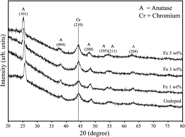
Glancing angle X-ray diffraction data of TiO2 films as function of dopant concentration
Summary of analytical data
From Fig. 1, it can be seen that the peak shifts of the principal (101) peak of anatase indicate that Fe doping caused lattice expansion, which can be attributed to the substitution of Ti4+ (ionic radiusVI = 0·075 nm) by Fe3+ (ionic radiusVI = 0·079 nm).14 The maintenance of charge balance that arises due to the substitute would require the formation of oxygen vacancies, and this can affect the band gap.15
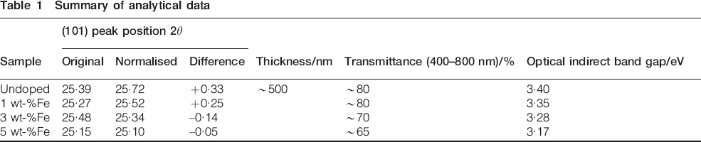
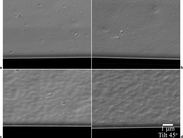
Figure 2 shows low resolution FIB cross-sectional images of the films. The thickness of the films was consistent and similar for all dopant concentrations. Furthermore, it can be seen that the surface roughness increased with increasing Fe dopant concentration. The surface morphologies were confirmed using high resolution FESEM images obtained at high magnification (×20 000), as shown in Fig. 3. The FESEM images show that the surface roughness, as suggested by the FIB images, was the result of shrinkage and subsequent cracking of the doped films. Previous studies have not reported shrinkage cracks for TiO2 thin films doped at similar Fe levels and fabricated by spin coating, although the precursors used were different.24, 27, 28
Single FIB images of TiO2 films as function of dopant concentration:
Images (FESEM) of TiO2 films as function of dopant concentration:
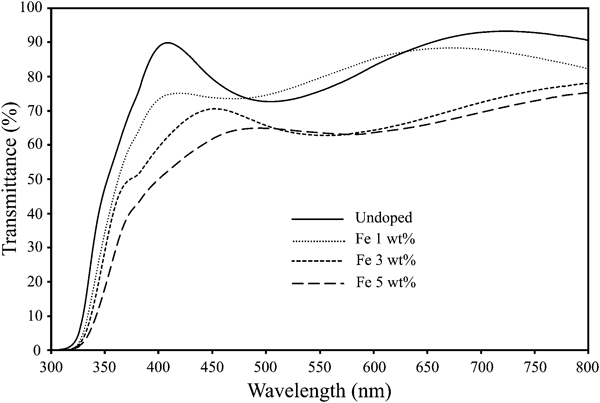
The transmittance data of the films produced in the current work are shown in Fig. 4. It is seen that the thin films reported in previous studies had higher transmittance compared to the ones obtained in the present work.24, 27, 28 Therefore, it can be concluded that these shrinkage cracks resulted in an enhancement of the scattering of light that consequently reduced the transmittance. The notable differences between the previous studies and the present work are that different metallorganic precursors were used and a drying stage at 75°C was absent in the former. Both of these factors are likely to have caused the observed differences in results with regard to shrinkage cracking.
UV–vis spectroscopy data of TiO2 films as function of dopant concentration
Optical indirect band gap data of TiO2 films as function of dopant concentration
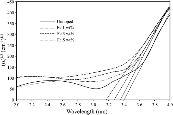
Figure 4 shows that the transmittance decreased with increasing Fe doping concentration, which is in agreement with previous works.24, 27, 28 In the present case, however, decreasing transmittance can be attributed to both increasing absorption by Fe and increasing scattering from the cracks. The optical indirect band gap of TiO2 films can be calculated using UV–vis spectroscopy data, the details of which have been described elsewhere.29 Figure 5 and the data in Table 1 suggest that the optical indirect band gap of the films decreased from 3·40 to 3·17 eV with increasing dopant concentration, similar to previous studies.24, 27, 28
It should also be noted that two other important factors could have contributed to the alteration of the optical indirect band gap, namely silicon contamination and thermal contraction stresses. Si4+ (ionic radiusVI = 0·054 nm), which is substantially smaller than Ti4+ (ionic radiusVI = 0·075 nm), could cause lattice contraction (with substitutional solid solution), which would negate the expansive effect of Fe3+ (ionic radiusVI = 0·079 nm).14 Alternatively, the entry of Si into the TiO2 lattice interstitially could cause lattice expansion. The effect of Si contamination of TiO2 films by substrates of soda lime silica glass26 and fused SiO2 (Refs. 23 and 30) has been reported previously. Since Si4+ and Ti4+ are isovalent, the lattice expansion and decreased band gap are consistent with interstitial solid solution formation (Si in TiO2). The presence of interstitial Si4+ (source of electrons) could raise the conduction band and the band gap, resulting in the measured value of 3·40 eV being higher than the commonly reported value of 3·20 eV for bulk anatase.5 However, such comparisons are obscured by the wide range of reported optical indirect band gaps for undoped anatase films, which range from 3·20 to 3·60 eV.23 With regard to thermal expansion cracking, the typical thermal expansions at 500°C are ∼8×10⁻⁶°C−1 for TiO2 (Ref. 31) and ∼5×10⁻⁶°C−1 for soda lime silica glass.32
The expansion of the film from the greater cooling contraction could cause lattice expansion of TiO2, resulting in a residual tensile stress on the film. Conversely, undoped TiO2 films on fused SiO2 (thermal expansion at 500°C of only ∼0·3×10−6°C−1)30 have been reported to show an increase in the optical indirect band gap to 3·40 eV (from 3·20 eV for bulk TiO2) owing to possibly residual compressive stresses.30 The authors’ explanation appears to derive from that of Thomas and Dube33 via Du et al.,34 who also used published band gap information (for SrTiO3) as a comparison. They33 speculated that intrinsic stress resulted in a raised energy configuration; however no physical rationalisation was provided for this possible state. These results raise the possibility of a direct relationship between residual stress and band gap (tensile stress→band gap decrease; compressive stress→band gap increase).
It is well known that the establishment of midgap states between the conduction and valence bands can decrease the band gap and increase the electrical conductivity.35 If midgap states exist, they probably are in the form of Fe donor bands and oxygen vacancy acceptor bands, which would explain the observed decrease in band gap in Fe doped films in the present work.
Yu et al.36, 37 also observed a decrease in the optical indirect band gap in Fe doped TiO2 films. They stated that the absorption in the visible region may be induced by a sub-band gap transition corresponding to the excitation of 3d electrons of Fe3+ to the TiO2 conduction band (charge transfer transition) at 415 nm and the d–d transition 2T2g→2A2g or 2T1g of Fe3+ or the charge transfer transition between iron ions (Fe3++Fe3+→Fe4++Fe2+) at 500 nm.
Summary
The present work reports the synthesis of Fe doped TiO2 thin films of ∼500 nm thickness by spin coating. Annealing at 500°C generated films comprised solely of anatase. The GAXRD data, normalised using the Cr (210) peak, indicate lattice expansion with increasing dopant concentration. However, drying at 75°C resulted in surface shrinkage cracking in the doped films only. This suggests that doping and drying were responsible for the cracking. Light absorption from Fe and scattering from the cracking are considered to be responsible for the decrease in transmission. The optical indirect band gap of the films decreased from 3·40 to 3·17 eV with increasing Fe dopant concentration, probably owing to the formation of midgap states, although residual tensile stress and Si contamination could be contributory factors. Since the mechanisms of crack propagation are closely related to the forming techniques used, further work is planned to investigate this aspect.
Footnotes
Acknowledgements
The authors are grateful for the financial support of the Australian Research Council (ARC), which have allowed this and other developmental work to be undertaken. The authors also would like to acknowledge access to the UNSW node of the Australian Microscopy and Microanalysis Research Facility (AMMRF).