
Abstract
Ba1−xSrxTiO3 (x = 0·3, 0·35) ceramics are fabricated by spark plasma sintering (SPS) technique and conventional sintering (CS) route. Their microstructures are determined together with the dielectric and ferroelectric properties. The grain sizes of SPS samples are smaller than those of CS. The differential scanning calorimetry data show that almost no latent heat associated with phase transition can be detected in the SPS sintered ceramics. Raman spectroscopy analysis suggests that the tetragonal phase increases with increasing the grain size, and the higher content of tetragonal phase leads the superior dielectric properties in CS sintered samples. Transmission electron microscopy analysis indicates that domain structure heavily relies on the grain size of ceramics. The poor ferroelectric properties of SPS ceramics are originated from the incomplete development of the tetragonal structure.
Introduction
Since ferroelectric barium titanate with high dielectric constant has been discovered in 1943, barium titanate based ferroelectric materials with perovskite structure are widely used in many manufactures. In addition, most of the applications make use of the dielectric behaviours of ceramics materials around the ferroelectric–paraelectric transition. The transition temperature TC of BaTiO3 can be efficiently adjusted by doping with different elements into the A and/or B site. Barium strontium titanate (Ba1−xSrxTiO3) is one of the compositions, and it has attracted a lot of attention in recent years. It is well known that pure barium titanate undergoes three successive phase transitions with decreasing temperature, namely from the cubic m3m to tetragonal 4mm, next to orthorhombic mm2 and to rhombohedral 3m phase, finally. For the transition temperature of Ba1−xSrxTiO3 ferroelectric transition, its compositional dependence can be described by an approximate relation1
In recent years, the main limitation in microelectronics applications is related to the stability of the polar phase as well as the presence of a high density of interfaces with reduction in spatial dimensions.7 It is known that the properties of ferroelectrics with fine grain sizes are often different and superior to those of conventional sintered materials with coarse sizes. However, high density Ba1−xSrxTiO3 with fine size is usually difficult to obtain because of the uncontrolled grain growth during the final stage of sintering process. There are some reports on the grain size effect of Ba1−xSrxTiO3 ceramics upon the dielectric properties.8–10 They just focus on the relationship between grain size and the dielectric properties, while the correction between the dielectric properties and ferroelectric domains is rarely mentioned. It is reported that poor development of ferroelectric domains results in the lower dielectric constant.11 Thus, the development of ferroelectric domains with varied grain size can be conducive to the production of Ba1−xSrxTiO3 devices with better properties.
Spark plasma sintering (SPS) is a process that makes use of a microscopic electrical discharge between particles under pressure. Compared with the conventional sintering (CS) method, SPS process enables a compact powder to be sintered under uniform heating to high density at relatively low temperature and in a much shorter sintering period, typically a few minutes. Shorter sintering period and lower sintering temperature carried out in SPS process are advantageous to suppress exaggerated grain growth.
In this study, highly dense Ba1−xSrxTiO3 ceramics are produced using SPS process. The grain sizes, ferroelectric domains and dielectric properties of SPS ceramics are compared with those of conventionally sintered ceramics. The relationship between grain size, ferroelectric domain and dielectric properties is also analysed.
Experimental
Ba1−xSrxTiO3 (BST, x = 0·3, 0·35) powders were synthesised via the conventional solid state reaction method. Stoichiometric mixtures of SrCO3 (99·9%), BaCO3 (99·93%), and TiO2 (99·5%) were milled for 24 h in anhydrous alcohol using zirconia balls media and calcined at 1150°C in air for 3 h to yield Ba0·65Sr0·35TiO3 (BST-35) and Ba0·7Sr0·3TiO3 (BST-30) powders. Then, the calcined powders were reground by hand in an agate mortar, placed into a graphite die and sintered under a vacuum of 6 Pa with an SPS apparatus (SPS-1050, SPS Syntex Inc., Kanagawa, Japan) for 5 min. The heating rate for Ba0·65Sr0·35TiO3 was 100°C min−1 from room temperature to 870°C, 40°C min−1 from 870 to 950°C and 20°C min−1 from 950 to 970°C, and the similar process was applied to Ba0·7Sr0·3TiO3 ceramics, except that the final sintering temperature is 980°C. The as sintered ceramics were finally annealed in oxygen for 6 h at the temperature of 1200 and 1250°C for BST-35 and BST-30 respectively. This treatment was used to guarantee relief of residual stresses and elimination of excess oxygen vacancies possibly produced during SPS process. For CS process, the calcined powders with 8% polyvinyl alcohols were pressed into pellets under a pressure of 98 MPa and subsequently sintered in air for 3 h at 1400 or 1415°C for BST-35 and BST-30 respectively.
The densities of the sintered samples were measured using the Archimedes method. Gold paste was used as the electrodes, and it was sputtered on both surfaces of BTS pellets. The dielectric characteristic of these ceramics were evaluated with a broadband dielectric spectrometer (Turnkey Concept 50, Novocontrol Technologies GmbH & Co. KG, Hundsangen, Germany) in a broad range of temperature (128–573 K) and frequency (1 Hz–10 MHz) with a heating rate of 2 K min−1. A differential scanning calorimetry (DSC) (204F1; Netzsch, Phoenix, AZ, USA) was used to detect latent heat during phase transition. The microstructure observation was carried on scanning electron microscope (SEM) (S-4800, Hitachi, Tokyo, Japan). Raman scattering spectra were obtained using an HR-800 Labor Raman (Jobin Yvon, France) at room temperature. The Raman spectrometer was equipped with a stigmatic single spectrograph, a Peltier cooled charge couple device detector and integral Raman microscope. The microscope attachment was an Olympus BX41 system and using excitation with Ar+ laser light (λ = 514·532 nm). The laser was incident on the samples in a 2 μm diameter spot through a standard ×50 microscope objective lens. The spectral resolution was about 1–2 cm−1. The samples for transmission electron microscopy (TEM) were prepared via the ultrasonic cutting of discs 3 mm in diameter and mechanical polishing to a thickness of ∼100 μm. The central portions of the discs were reduced further to ∼10 μm by mechanical dimpling (Model 656, Gatan, San Francisco, CA) followed by final polishing. The final perforation of the sample was conducted via precision argon ion milling (Model 691; Gatan, San Francisco, CA, USA) using an acceleration voltage of 4 kV. In order to prevent the surface charging, the perforated sample was coated by a thin carbon film using precision etching coating system (Model 682; Gatan). The selected area electron diffraction patterns, microbeam electron diffraction patterns and high resolution lattice images were obtained at 300 kV by a high resolution TEM (Tecnai F30 G2; FEI, Oregon).
Results and discussion
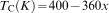
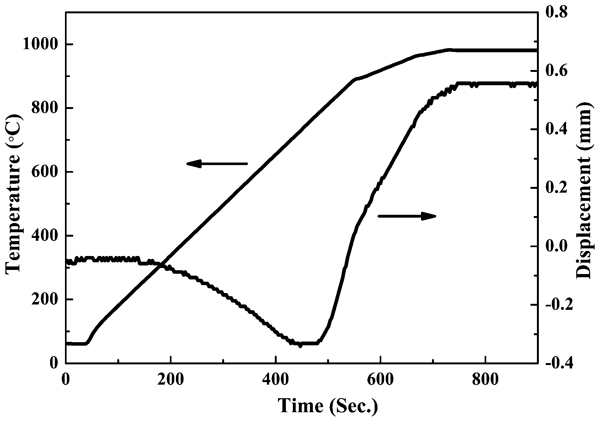
Figure 1 shows the sintering behaviour of the BST-30 ceramics during SPS. The samples expand gradually with an increase in temperature up to 800°C, and then it shrinks. The shrinkage increases rapidly as the temperature increases from 825 to 960°C. During the soaking period, only a very small shrinkage was observed, indicating that the densification was almost completed at temperatures <960°C. It is said that the rapid sintering by SPS depresses the grain growth of polycrystals. The sintering behaviour of the BST-35 ceramics is similar to that of BST-30 ceramics. Both the relative densities of BST-35 ceramics and BST-30 ceramics sintered by SPS process are >99·6%, suggesting that a relatively low sintering temperature of 980°C is enough for the densification of BST ceramics by SPS. Although the local temperature of the sample is slightly higher than the sintering temperature measured near the surface of the die, it should be noted that the densification temperature of SPS is ∼400°C lower than that of the CS samples. This can be attributed to the microscopic electric discharge between particles and the application of mechanical pressure during SPS.12–15 In the initiate period of SPS process, the microscopic electrical discharges between particles clean the surfaces of particles from the absorbed species and activate the surface. The cleaned and activated surfaces enhance the diffusion, promote the transfer of material and quickly densify the sample. On the other hand, the application of mechanical pressure aids in removing pores and enhancing the diffusion. The SEM microstructures of the polished and thermal etched surfaces of BST samples sintered by SPS and CS are shown in Fig. 2. For SPS samples, there are few pores on the surfaces of both BST-35 and BST-30 ceramics, which is consistent with the fact that both samples have nearly 100% theoretical density. In contrast, there are some pores on the surfaces of CS sintered samples, and the relative densities are ∼97% theoretical density. The average grain sizes of CS sintered BST-35 samples (∼40 μm) are much larger than those of SPS sintered samples (∼0·9 μm), and so do in BST-30 ceramics.
Shrinkage curve and sample displacement as function of sintering time during SPS of BST-30 ceramics
Images (SEM) of polished and thermal etched surfaces of BST ceramics: a SPS BST-35 sample; b SPS BST-30 sample; c CS BST-35 sample; d CS BST-30 sample
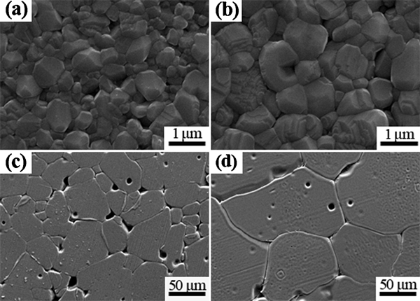
Figures 3 and 4 show the temperature dependence of the dielectric constants and dielectric losses for BST-35 and BST-30 ceramics at various frequencies (1, 5, 10, 50, 100, 500 and 1000 kHz) respectively. Only a diffuse peak can be observed on the curve of temperature dependence of dielectric constants of SPS sintered samples, which should be induced by the transition from paraelectric to ferroelectric phase. While there are three sharp peaks on the curves of CS sintered samples, and they should be related to three phase transitions from high to low temperature in turn: cubic paraelectric to tetragonal ferroelectric phase, tetragonal to orthorhombic phase and orthorhombic to rhombohedral phase. In BST-35 ceramics, the corresponding Curie points are 294 and 290 K for SPS and CS samples. While in BST-30 ceramics, they are 308 and 306 K. For these two compositions, the maximum dielectric constants around the Curie points of SPS sintered samples (∼6000) are much smaller than those of CS sintered samples (∼18 000). In contrast to SPS sintered ceramics, the CS sintered ceramics exhibit a sharp anomaly of dielectric constant and a large dissipation near the phase transition temperature. As shown in insets of Figs. 3 and 4, the degree of diffusivity in the above compositions states that the dispersion of SPS sintered samples (1·74 for BST-35 and 1·65 for BST-30) are larger than those of CS sintered samples (1·16 for BST-35and 1·15 for BST-30). Figure 5 gives the DSC data for BST ceramics. Clearly, there are distinct differences between the samples prepared by SPS and CS methods. The DSC data show that three endothermic features near 200, 250 and 310 K for CS specimens are attributable to three first order transformations, which is consistent with the result based on the dielectric constant data. However, almost no latent heat associated with phase transition could be detected for the SPS sintered ceramics, which indicates that they almost do not contain any regions with a sharply defined phase transition in SPS sintered BST grains. The result shows that the grain size has a profound impact on the phase transition behaviour of the present ceramics.
Temperature dependence of dielectric constants for BST-35 ceramics: dielectric constant for a SPS and b CS and dielectric loss for c SPS and d CS; insets show relation between ln (1/ϵ−1/ϵmax) and ln (T−Tm) for BST-35 indicating 1·74 and 1·15 respectively
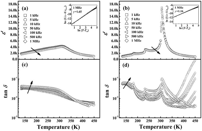
Temperature dependence of dielectric constants for BST-30 ceramics: dielectric constant for a SPS and b CS and dielectric loss for c SPS and d CS; insets show relation between ln (1/ϵ−1/ϵmax) and ln (T−Tm) for BST-30 indicating 1·65 and 1·16 respectively
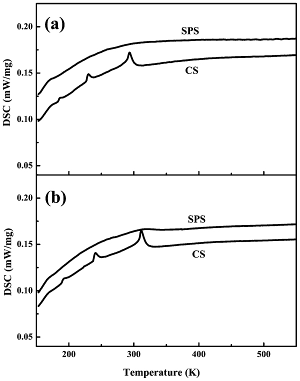
Data (DSC) for BST ceramics fabricated from CS and SPS methods: a BST-35; b BST-30
Raman spectra of BST ceramics with the frequency range of 100–800 cm−1 are shown in Fig. 6, which are used to further confirm the results of the dielectric characteristics. All samples show similar spectra, which are in agreement with those reported previously for tetragonal or orthorhombic phases.16 In the spectrum of BaTiO3 sample, a positive intensity Raman peak at ∼180 cm−1 usually can be observed in the orthorhombic phase, while a negative peak is indicative of a tetragonal phase.17 The intensity of the Raman peak, which indicates the ratio of the tetragonal phase, increases with increasing grain size. It is reported18–21 that the dielectric properties are influenced greatly by the internal stress produced by the phase transformation from cubic to tetragonal type. The dielectric constant of BST ceramics can be regarded as the sum of a volume contribution, which is based on the single crystal dielectric constant and of the contribution of the ferroelectric domain walls in the electric field.22

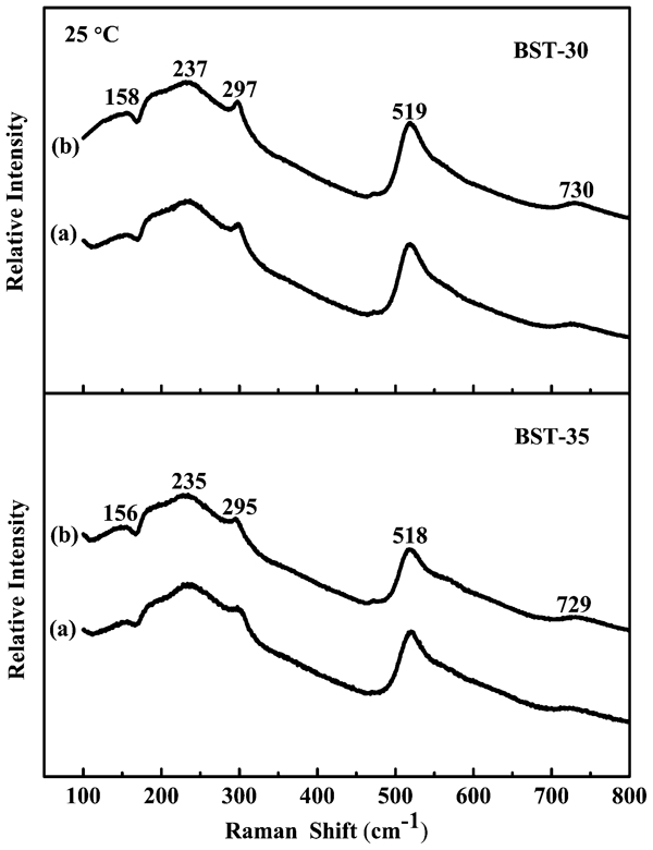
Raman spectra for BST ceramics processed by SPS and CS methods: a SPS; b CS
Considering the competition between constrained cubic and tetragonal strain, it is worth well to further research the grain size dependent structure characteristics of Ba1−xSrxTiO3 (x = 0·30, 0·35). In order to release the stress induced from the transition from cubic to tetragonal phase in barium strontium titanate, the 90° domains will be formed in the crystal. Figure 7 shows that the ferroelectric domain structure is strongly dependent on grain size. Two regions of the vertical polarisation direction constitute the 90° domain with intersecting 90° domain boundary, which is shown in Fig. 7a and b. The fewer domains can be observed in the SPS sintered samples, which means that the less area of the domain wall per volume is presented in the ceramics. The lower density of domains walls in SPS sintered samples contributes less to the dielectric constant and results in the smaller dielectric constant. On the other hand, with decreasing density of domain wall, it is difficult to eliminate the stress within the grains, which make the phase transition more difficult. Figure 7c and d shows the 180° domains in the ceramics prepared by SPS and CS methods respectively. The observed 180° domain sizes in the SPS samples are significantly smaller than those of the CS samples. The domain width of SPS sintered samples is ∼45 nm, while that in CS sintered samples is ∼196 nm. This difference is mainly due to the grain size effects. Within the crystal surface, domains nucleate from the vicinity of the grain boundary of ceramics, grow toward the grains plane and terminate inside the grains or penetrate the grains. With the grain size decreasing, the formation of domain is hindered by the increasing grain boundaries, so the domain size in SPS sintered samples is smaller. Just because of the poor development of ferroelectrics domains in SPS sintered samples, their ferroelectric performances become deterioration.
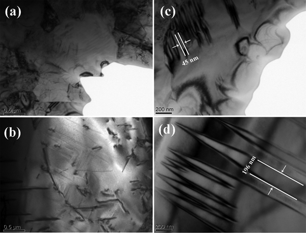
Photomicrographs (TEM) illustrating development of ferroelectric domain structure for BST-30 ceramics processed by SPS and CS methods: a SPS, 0·5 μm; b CS, 0·5 μm; c SPS, 200 nm; d CS, 200 nm
In order to confirm the development of the ferroelectric domains, ferroelectric hysteresis loops of these samples are carried out at room temperature and then shown in Fig. 8. All samples exhibit P-E hysteresis loops, without poling. The contribution of ohmic losses can be negligible because of the high resistance of the samples, >1 GΩ.28 The shape of the hysteresis loop depends substantially on the grain size of the samples. For BST-30 ceramics, the spontaneous Ps and remanent Pr polarisations of the SPS pellets (Ps = 11·70 μC cm−2, Pr = 1·29 μC cm−2) are smaller than those (Ps = 14·20 μC cm−2, Pr = 4·18 μC cm−2) in the CS pellets as a consequence of the presence of 90° walls that are moved by the electric field. The rectangular ratio of the hysteresis loops, which is defined as Pr/Ps,29 decreases with grain size, i.e. from 0·29 to 0·11 for CS and SPS samples respectively. The same consequence is also found in BST-35 ceramics. The smaller Pr, Ps and Pr/Ps values for SPS specimen suggest poor development of the ferroelectric domains.30 It is to say that tetragonal structure develops poorly and a local orthorhombic structure exists in SPS sintered samples, which is consistent with the results of Raman spectra and TEM. It is noticed that the estimated coercive field Ec in SPS sintered samples (1·61 and 1·40 kV cm−1 for BST-35 and BST-30) is higher than that in CS sintered samples (0·62 and 0·86 kV cm−1 for BST-35 and BST-30 samples). This can be attributed to the much larger grain boundary areas due to the smaller grain size of the samples that obstructs domain movement under an external electrical field.31, 32
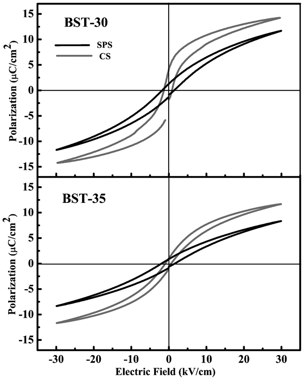
Ferroelectric hysteresis loops of BST ceramics processed with SPS and CS conditions at room temperature
Conclusion
Highly dense BST ceramics are obtained by the SPS method. Their microstructures are determined together with the dielectric and ferroelectric properties. The average grain size in the SPS samples is <1 μm, which is much smaller than that in the CS samples. Raman spectroscopy analysis suggests that the tetragonal phase increases with increase in the grain size. The different ferroelectric properties between SPS and CS ceramics originate from incomplete development of the tetragonal structure as well as the presence of a local orthorhombic structure.
Footnotes
Acknowledgements
This work was supported by the Natural Science Foundation of China under grant nos. 51272233 and 50832005 and by the National Basic Research Program of China under grant no. 2009CB623302.