





Abstract
The science of surface plasmon polaritons, known as “plasmonics,” is reviewed from the viewpoint of applied spectroscopy. In this discussion, noble metals are regarded as reservoirs of photons exhibiting the functions of photon confinement and field enhancement at metallic nanostructures. The functions of surface plasmons are described in detail with an historical overview, and the applications of plasmonics to a variety of industry and sciences are shown. The slow light effect of surface plasmons is also discussed for nanoimaging capability of the near-field optical microscopy and tip-enhanced Raman microscopy. The future issues of plasmonics are also shown, including metamaterials and the extension to the ultraviolet and terahertz regions.
INTRODUCTION
Spectroscopy has been fundamental in the development of physics, chemistry, and astronomy. It has significantly contributed to progress in biology, medicine, materials science, and electronic engineering. It is now also playing a key role in nanoscience. In this article, I will review the spectroscopic responses of metallic nanostructures to photons. This field of science has been known as the study of optical properties of metals in solid-state physics but is now called “plasmonics” and is being studied as part of cutting-edge nanotechnology research in conjunction with advanced nanotechnologies and nanomaterials.
In the 1970s, the development of mathematical methods and algorithms for super-resolution exceeding the classical diffraction limit became one of most exciting topics in the optics field for microscopy and astronomy1,–7. A number of methods have been developed with use of large-scale computers to recover the missing information lost through optical imaging systems. An image of a human face can be mathematically constructed from a photograph of an eye as a part of the face with a computer; even a world photo map can be reconstructed from a single photograph of a site. 8 Although powerful computers are now available, there are still many issues in solving the inverse problems, such as dynamic range, noise, and detection limit caused by the detectors, and stable light sources used for measurement. These days, scientists spend more time using instruments and high technology for nanoimaging than for developing mathematics.
In the 1980s, scanning tunnel microscopy 9 and atomic force microscopy (AFM) 10 were invented, and atoms and molecules were directly visualized. The optical version of scanning probe microscopy was developed in 1985 independently by two groups.11,12 In 1992, the author proposed a near-field scanning optical microscope using a metallic probe. 13 This was published in 1994 with experimental results. 14 I used surface plasmon polaritons (SPPs) that exist at the tip of a metallic probe with near-field photons in nanometer scale. A conventional optical microscope requires glass lenses, whereas a near-field scanning optical microscope uses a metallic probe. The resolution of a conventional optical microscope is determined by the size of the objective lens (or more precisely the numerical aperture of the lens), whereas that of a near-field scanning optical microscope is determined by the tip diameter of the metallic probe. In this paper, I first review the science of SPPs, and then of nanoimaging and nanospectroscopy, before tackling the limitations and future issues of plasmonics.
METALS AS RESERVOIR OF PHOTONS: SURFACE PLASMON POLARITONS
Noble metals, particularly gold and silver, fascinate people of all ages and cultures. They shine brilliantly when polished and can be used as mirrors in the infrared and visible regions, respectively. They are also used in jewelry and as currency. Noble metals also have been used in electrical devices and materials because of their high electric and thermal conductivity as well as high ductility. All of these characteristics are attributed to the free electrons in noble metals. At the nanometer scale, the properties of such metals make them even more attractive for use in advanced devices, and this is the main topic in this paper.
Metals can be considered to be a “sea” of free electrons. The surface wave on this sea is known as a surface plasmon, or the collective oscillation of free electrons. The dispersion relation between wavenumber, k, and frequency, ω, of a surface plasmon polariton (SPP) is given by
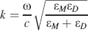
Figure 1a shows the dispersion relation for SPP given by Eq. 1 and that for propagating light. The wavenumber of the surface plasmons is always greater than that of the propagating light. In other words, the electromagnetic waves generated by the oscillation of electrons at the metal surface have a wavenumber different from that of propagating light, so that such light does not propagate in the medium but is localized in the vicinity of the metal surface. This is a reason why plasmonics is based on near-field optics. 16

(a) Dispersion relations of propagating light and surface plasmon polariton (SPP). c, ωSP, εM, εD, and kpr denote the light velocity in vacuum, angular frequency of SPP resonance (which is described as ωp/√2 under the Drude's free-electron model, where ωP is plasmon frequency), complex dielectric constant of metal, dielectric constant of surrounding medium, and wavenumber of propagating light, respectively. K represents the change of the wavenumber due to a periodic nanostructure (periodicity: 2π/K), which enables coupling of propagating light to SPP. (b) Reflection of propagating light on metal surface. (c) Coupling of propagating light to SPP by a nanostructure, and reconversion of SPP into propagating light by another nanostructure.
When propagating light is incident on the metal surface, electrons move to erase the incident electromagnetic field, resulting in the generation of a reflection (Fig. 1b). Here, the propagating light incident on the metal does not excite surface plasmons. This is because the surface wave (the electromagnetically near-field wave) and propagating wave (radiant field) have different wavenumbers with respect to the frequency. In order for the propagating light to induce the excitation of SPPs, a periodic structure with a grating vector corresponding to the difference between the wavenumber for SPPs and that for the incident light in the surface direction should be formed on the metal surface. Using this structure, incident light energy is transferred to that of SPPs and then the reflection is reduced significantly. At this point, the metal serves as a reservoir of photons rather than as a reflector of light. The light energy stored in reservoir can be reused. Indeed, the plasmon energy stored at metal surface with periodic or rough structure can be extracted as photons (Fig. 1c).
The function of a metal surface serving as a reservoir of photons will likely be applied to solar cells and lasers. Although some projects for plasmonic solar cells were pursued in 1990, 17 they were not popularized by the commercialization process, which favored other solar devices. Plasmonic solar cells are now attracting renewed attention, but there was no particular fundamental progress in research and development since the above project was proposed. Plasmonic lasers have recently been intensively and competitively studied and developed;18,–22 however, the absorption loss has not been completely overcome.19,20 Plasmonic light-emitting diodes are closer to commercialization.23,24 Figure 2 shows the schematics of our proposed plasmonic band gap laser with experimental results. 18 The configuration of this plasmonic laser is based on a plasmonic crystal with a periodic structure on a metal surface (Fig. 2c). In the dispersion relation of the periodically corrugated metal surface, a band structure is generated, indicating that plasmons at a frequency inside the band gap would be confined on the surface but do not propagate on the surface in two dimensions. Vertically, SPPs are confined in the near field from the surface as an evanescent field. If the plasmonic field enhancement exceeds the addition of the absorption and the scattering loss, lasing at the frequency corresponding to the edges of band gap may be introduced.19,20

Plasmonic laser. (A) Mechanism of plasmonic laser. (B) Dispersion relation of SPP on plasmonic crystal. A band gap is present at the wavenumber of k = π/Λ (Λ = lattice constant). (C) Topographic image of a plasmonic crystal fabricated by two-beam interference photolithography. (D) Fluorescence spectrum of DCM film on a plasmonic crystal. Intensity of fluorescence from the DCM molecules is enhanced in a particular wavelength region, compared with that from DCM molecules without plasmonic crystal.
Surface plasmon polaritons can also be excited with propagating light (i.e., coupled with propagating light) in the case of finite structures of metal such as nanowires and nanoparticles, where SPPs exist as standing waves that remain on a limited part of the surface as a cavity resonator, rather than propagate on the surface. The resonant frequency (or wavelength) of SPPs for the structure is a function of length or diameter. 25 SPPs at such finite structures are called localized surface plasmon polaritons (LSPPs). For a sphere sufficiently smaller than the wavelength, the tered light is enhanced more strongly for rods, dimers, and aggregates than for single spheres. It has been reported that nanogap structures represented by dimers and dipole antennas also exhibit an extremely high enhancement.30,31
Research on plasmonic metallic nanostructures, not only on the applications to SERS, has made considerable progress in the last decade. Halas and Nordlander and coworkers analyzed the modes of various metallic nanostructures and demonstrated that metallic nanoshells have a resonance mode in the near- and mid-infrared ranges.32,–34 Photodynamic therapy using metallic nanoshells has been commercially used as a practical application of this principle. 34 Durr demonstrated two-photon luminescent imaging of unlabeled cancer cells using gold nanorods. 35 The group led by Xia synthesized various nanostructures such as nanocubes, nanocages, nanobelts, and nanorice by the reduction method with appropriate surfactants.36,37 Hao et al. 38 and Hecht et al. 39 made nanostars and bow-tie antennae (dimers), respectively. Kottmann et al. analyzed hot spots formed at nanotriangles in detail, 40 and Futamata et al. reviewed the field distribution and the enhancement at nanostructures. 41 The field distribution near a probe was shown by using the finite-difference time-domain (FDTD) method, and the effect of the interaction between probe and samples has been discussed.42,43
The above research eventually boils down to resonance mode analysis and photon localization as hot spots. For obtaining a localized hot spot at a single wavelength, a simple nanorod would be the most appropriate with dipole antenna resonance, whereas nanoparticles or nanorods not connected to each other but separated from each other with very small distance are preferable for achieving field enhancement in broad bands. 44 For a dimer or a bow-tie antenna, a hot spot is formed in the gap between the two components with a very strong field; however, the application is limited to the situation when the sample can be inserted into the gap. A simple dipole antenna probe is reasonable to use for the microscopic observation of arbitrarily distributed samples, because such a probe can easily be brought close enough to the sample on any kind of substrate.14,45
SOMMERFELD AND WOOD
Plasmonics has been studied for over 100 years. In 1899, Sommerfeld predicted that electromagnetic surface waves propagate along a thin metallic wire. 46 More than 100 years after, in 2005, Ditlbacher and colleagues observed surface plasmon polaritons (SPPs) propagating along thin metallic nanowires using an optical near-field microscope. 47 In 2003, Maier and colleagues realized the propagation of plasmons along nanoparticles arranged in a line. 48 Here, the propagation is made with localized-mode SPPs via gaps. I proposed the image transfer with metallic nanorods array in nanometer resolution. 49 When the nanorod array is tapered, the array works as a magnifier. 44
In 1902, optical scientist Robert Wood, observed a dark line in a spectrum of light dispersed at a grating (now known as Wood's anomaly). 50 This was because the higher-order evanescent diffracted light was coupled with SPPs, resulting in the transfer of energy to the SPPs, i.e., the lower-order diffracted light (propagating light) lost its energy. Because the surface of the grating happened to be wet owing to contact with water, Wood by chance observed an unusual phenomenon that had not been observed in ordinary diffraction experiments. Moreover, by observing the movement of the dark lines, he confirmed that the refractive index gradually changed with the addition of glycerin to water. This experiment was the origin of commercially available surface plasmon resonance (SPR) sensors, or even more advanced than those of current sensors. In 1988, I published a paper describing a surface plasmon sensor that can obtain angular spectra using a spatially extended light source (a light-emitting diode) without scanning in the angular direction.51,52 I also reported a high-sensitivity sensor with a multilayer structure in the long-range mode, 53 a Wood-type sensor, 54 and a two-photon-excited surface plasmon sensor. 55 I compared the SPR sensor to other refractometers in terms of accuracy and sensitivity in their refractive index measurement for practical samples that absorb and/or scatter light.56,57 In 1995 I patented a surface plasmon microsensor array (similar to what is currently called a biochip), 58 approximately 90 years after Wood's report.
In 1904, two years after Wood's paper, Maxwell-Garnett reported the spectroscopy of metallic nanoparticles in dielectric materials. 59 He demonstrated that the complex dielectric constant of a material changes with the dispersion of metallic nanoparticles. This revealed that the red color of stained glass originates from gold nanoparticles in the glass. It was also explained that the color of stained glass depends on the size of the nanoparticles.
In 1908, four years after Maxwell-Garnett's report, Mie solved the Maxwell's equations of electromagnetism in polar coordinates under boundary conditions for a system in which plane waves are scattered in a sphere. 60 This is the well-known Mie scattering theory. According to this theory, the scattering field is the sum of the nonradiative nearfield components localized near the sphere and the radiative components that propagate far from the sphere. 61 Even now, over 100 years after the reports by Maxwell-Garnett and Mie, research on the above theories is still playing a key role in the optical science of nanoparticles.
PHOTONS WITH VELOCITY OF ZERO: TIP-ENHANCED RAMAN SCATTERING (TERS) MICROSCOPY
The momentum (wavenumber) of surface plasmon polaritons is greater than that of photons propagating in free space, i.e., the wavelength of SPPs is shorter and the velocity of SPPs is lower than that of photons. In short, a microscope or a fabrication system using SPPs provides a spatial resolution higher than any conventional optical microscopes or lithography systems, which have a strict resolution limit due to diffraction. The momentum (wavenumber) of SPPs further increases as the frequency increases from the visible range to the resonant frequency of the surface plasmons (ωSP) in the ultraviolet (UV) range, which causes a decrease in the velocity of the surface plasmons (see Fig. 1a). According to the experimental result obtained by Smolyaninov, the wavelength of the propagating light decreases from 502 nm to 70 nm on the surface of a metal. 62
Ultimately slow photons have a wavelength of 0 and velocity of 0. As shown in the dispersion relation in Fig. 1a, the momentum (wavenumber) of SPPs becomes infinitely large at their resonant frequency and the velocity becomes zero. The super-lens (or the perfect lens) proposed by Pendry is in this state. 63 Super-lenses appear to enable the realization of microscopes with an infinitely high resolution because of the zero wavelength (in fact, the optical spot broadens because of absorption). However, an image formed by a super-lens is not detected by human eyes or by a charge-coupled device camera, because it is localized at the surface of a metal as a nonradiative near-field light image, which cannot be seen in the far field with propagating light. Zhang and his colleagues coated the metal surface with photoresist film to record such a near-field image to be observed with atomic force microscopy (AFM). 64 If one wants to use photoresist film to record the near-field light distribution, he/she may coat it directly on the sample, and a plasmonic film is not necessary. 65
I invented a SPP microscope using a metallic nanoprobe rather than using a thin metallic film. 14 In this microscope, it is not necessary to adjust the wavenumber of surface plasmons (near-field light) to that of the propagating light when the metal surface is sufficiently smaller than the wavelength (Fig. 3a). Localized surface plasmon polaritons (LSPPs) are induced in the tip of the nanoprobe. Light in a space smaller than the wavelength can be, even remotely, detected by bringing the metallic probe close to the near field of a sample. An image is obtained by scanning the metallic probe along the sample surface. This configuration is called a scattering near-field optical microscope or an apertureless near-field optical microscope. The electric field is markedly enhanced in the vicinity of the tip apex of the probe due to the resonance of LSPPs (Fig. 3b). The metallic probe is fabricated by either electrochemical etching of a metallic wire or by vacuum deposition or electroless plating on a silicon probe.66,67

TERS microscopy. (A) Coupling of propagating light to localized surface plasmon polaritons. (B) Spatial distribution of light intensity in vicinity of a metallic tip apex, calculated by finite-difference time-domain method (FDTD). Light is confined in a space much smaller than wavelength of propagating light. (C)–(D) Raman images of a DNA network structure, which are constructed by signals of tip-enhanced coherent anti-Stokes Raman scattering light (C) at a molecular vibration frequency (1337 cm−1) of adenine in the sample DNA, and (D) ata frequency (1278 cm−1) that does not correspond to any molecular vibration frequency of the sample. (E) Line profile along a line indicated by the two arrows. The spatial resolution of 15 nm was achieved.
This microscope is particularly effective for Raman scattering imaging of the distribution of molecules. I also first reported the Raman imaging application of this microscope,68,45 now called the TERS microscope. 69 LSPPs at the tip apex of the metallic probe contribute to the increase of the scattering power through both excitation and scattering processes. The TERS microscope can be considered to give point-by-point Surface-enhanced Raman scattering (SERS) detection of a distributed sample to form a Raman image with nanometer resolution. Coherent anti-Stokes Raman scattering has been combined with the TERS microscope for imaging of DNA at a spatial resolution of 15 nm and a million fold field enhancement (Figs. 3c, 3d, and 3e). 70 An article by Volker Deckert on the current state-of-the-art of TERS is slated for an upcoming article of this journal. An isolated metallic nanoparticle has been also used instead of a metallic needle probe as a plasmonics probe, the position of which was precisely controlled and scanned relative to the sample at the beam focus of a trapping laser. 71
FUTURE OF PLASMONICS: IMPROVING THE RESOLUTION BEYOND 1 NM
Since a plasmon is given by the collective oscillation of free electrons within a metal, a plasmon exists in a metal crystal with many atoms; there is no plasmon in an isolated single metal atom. This requirement limits the size of the metallic probe, and hence the spatial resolution of this microscope. However, a spatial resolution exceeding this limit is required in the fields of nanoscience and bioscience, and advanced nanomaterials and nanodevices.
One possible way to make a breakthrough in the resolution limit of plasmonics is the use of the chemical effect, which is seen when the metal and sample are nearly in contact with each other or the interaction distance is less than 1 nm. Chemical adsorption of a molecule to the metal particle contributes to the enhancement of Raman scattering in addition to plasmonic (electromagnetic) enhancement.72,73 I confirmed that the intensity and shape of Raman spectra markedly changed when a metallic probe was brought very close to molecules forming complexes (Fig. 4a). 74 For single molecule detection, the adsorption site of a molecule to the probe changes in time, resulting in changes of the Raman spectrum with time. 75 Figure 4b shows the spectral change during the measurement of adenine molecule with a metallic tip, which can be seen because of the high position accuracy of the tip. 76 This experiment requires a probe with an extremely high accuracy in regulating the distance between the probe tip and the sample molecules and for the detection of Raman spectra, which was realized by combining a time-gate method with a photon-counting method, i.e., a time-gated photon-counting scheme.77,78

Beyond the limitation of plasmonics. (A) Raman spectra of adenine-silver isomers, which were calculated by density function theory. 74 (B) Waterfall plot of time evolution of TERS spectrum of adenine. The gray scale corresponds to Raman intensity, and Raman spectra are plotted as a function of time (the vertical axis). The intensities and peak positions of the Raman spectra change with time. 76 This result indicates the possibility of the single molecule sensitivity of TERS spectroscopy of DNA base molecules. (C) Change of TERS spectra of a single-walled carbon nanotube (SWCNT) by a tip-applied pressure. 79 (D) Change of TERS spectra of C60 fullerene by a tip-applied pressure. 80 (E) (a) An isolated single-walled nanotube (SWNT) was scanned in steps of 1 nm under a constant tip-applied force of 2.4 nN. (E) (b) The line profile shows the peak shifts (black dots) as a function of the tip position measured from the SWNT, and corresponding best fit (red line) for the scan is shown by line in (E) (a). (F) (a) An AFM image of a two-dimensional nanocrystal of adenine. A metallic tip was scanned across the sample edge in the direction of the arrow under a tip-applied pressure of 0.3 nN. (F) (b) The line profile of the shift in RBM of adenine along the scan direction. The steep edge of the line profile shows a spatial resolution of about 4 nm.
Another method to attain resolution beyond the limit of plasmonics is the use of force between a sample and the probe. When a TERS probe applies pressure on the sample locally under the probe tip, the Raman spectrum of a sample would locally change due to the local distortion of the sample. The distortion area can be much smaller than the diameter of the probe apex by controlling the pressure precisely, and individual molecules are deformed one by another with the increase of the force on the sample.74,79 I confirmed that the Raman spectra of carbon nanotubes, C60 fullerenes, and DNA base molecules were changed by the probe (Figs. 4c and 4d).74,79,80 Figures 4e and 4f show atomic force microscopy (AFM) images and line profiles (one-dimensional images) of an isolated single wall carbon nanotube and adenine nanocrystal obtained with the pressure-assisted TERS microscope. 81 The spatial resolution was ∼ 4 nm for both results. The theoretically calculated contact area between the probe and samples was as small as 0.3 nm 2 when using the microscope, which indicates the further possibilities of Raman imaging for the base pairs of DNA molecules. 82
SPECTRAL RANGE OF PLASMONICS AND METAMATERIALS
Gold and silver are plasmonic materials in the visible and infrared regions, while they behave as dielectrics in the ultraviolet (UV) range above the plasmon frequency. However, there is a potential for many applications of plasmonics to the deep-UV region, including resonant surface-enhanced Raman scattering (SERS), 83 resonant Raman bio imaging, 84 and nanolithography. Aluminum is plasmonic in the UV, but not in the visible spectrum. I have developed a deep-UV tip-enhanced Raman scattering microscope for DNA base imaging using an aluminum tip. 85 In the ranges from radiowave to farinfrared (terahertz) light, gold, silver, and other metals are almost perfectly conductive but not plasmonic. In such ranges, the dispersion curve of surface plasmon polaritons is very close to that of the propagating light (Fig. 1a), i.e., the wavelength of SPPs is almost the same as that of the propagating light. Therefore, field enhancement and nanometer scale localization of photons cannot be induced with metals in terahertz and microwave ranges. Combining metal and dielectrics in fine structure, however, induces a pseudo-plasmonic effect in wavelength ranges other than the visible range, 86 and such a plasmon-like quantum is called a spoof plasmon. 87 This pseudo-plasmonic structure may refer to metamaterials 88 or structural birefringence. 89
Metamaterials, which recently were enthusiastically accepted by optical scientists, are artificially fabricated material structures with a number of simple and small metal components. 88 They exhibit extraordinary optical properties including negative refraction and invisibility. Metamaterials use plasmonic properties, i.e., wavelength shortening, near-field photon localization, and field enhancement in their applications, whereas in the microwave range they are considered as array antennae made of conductive metallic wire units such as Yagi-Uda antenna. 90 Free electrons move at the speed of light in metals as a conductor in the microwave range, so that the wavelength reduction will not be seen.
There have even been proposals on the application of metamaterials to fighter planes that are invisible to radar (invisibility cloaks).91,92 I controlled the relative magnetic permeability by arraying metallic resonators (split-ring resonators) within a dielectric, and I developed a material with a negative refractive index and a loss-less material that does not reflect light at its surface (Fig. 5a).93,94 Fabrication of metamaterials is currently one of the main issues in achieving such applications in the visible range. A method of fabricating resonator arrays by the two-photon–induced reduction of metal ions using a tightly focused laser has been reported (Figs. 5b and 5c).95,96

(A) Metamaterial for controlling only μ of the s-polarization component of incident light, which responds to magnetic field penetrating through the split-ring resonators. The magnetic permeability is no longer 1. (B)–(C) Silver nanostructures fabricated by two photon-induced reduction method.
FINAL REMARKS
In recent years, many meetings and sessions on plasmonics have been held around the world. Researchers of physics, chemistry, biology, electromagnetism, and devices have been establishing a network across various fields and countries. I believe that new science will be born from such a new community that will not be limited by conventional barriers between fields of science and between countries.
Footnotes
ACKNOWLEDGMENTS
The original version of this article was published in Japanese in Bunko Kenkyu (Journal of the Spectroscopical Society of Japan) in June 2009, as a summary note of the Society Award Lecture delivered in the Annual Meeting of the Spectroscopical Society of Japan, in November 2008. Applications of plasmonics are also found in other review articles97,–99 along with original papers I have written.100,101 I express my deepest gratitude to Taro Ichimura, currently at Riken Quantitative Biology Center, Osaka, for his valuable discussions.