





Abstract
Operations scheduling and Lookup Table (LUT) based technology mapping are fundamental problems of mapping designs onto an electronic device, such as a Field Programmable Gate Array. We present an approach to apply two optimizations consecutively. As first optimization, we apply several metaheuristic algorithms for multi-objective optimization at the High-Level Synthesis stage. As a second optimization, we realize reductions of LUTs at the Logic Synthesis stage. Several circuit designs are represented in a Data Flow Graph (DFG) and the experiments are carried out on the standard Mediabench benchmark. In the first optimization, we compared NSGA-II, FEMO, HypE, IBEA, SPEA2 and WSGA. Results have an average improvement 14.06% in occupied Area and 7.01% in Power consumption. Then, optimized DFG schedules are converted into Very High Description Language code using the Xilinx ISE Design Suite tool. Later, in the second optimization, The IMap algorithm is used to obtain combinational area reductions. Results show that 60% of the circuits are improved in comparison with the Xilinx ISE Design Suite.
Introduction
The Field Programmable Gate Array (FPGA) is a semiconductor device containing logic blocks whose interconnection and functionality can be configured in situ using a High Description Language (HDL), Very High Description Language (VHDL) or Verilog. FPGAs are characterized as programmable or reconfigurable, and it is precisely this property that distinguishes them from other similar devices, like an Application-Specific Integrated Circuit (ASIC). Actually, FPGAs are used in countless scenarios; for example, robotics and household appliances [8,32]. The FPGAs contain Configurable Logic Blocks (CLB), Input/Output Blocks (IOB) and several types of connections: direct connections, general purpose connections and long distance lines. Optimizing the manner in which these connections are made it is possible to reduce the resources used by the FPGA device. This is a non trivial scientific problem to be treated [28].
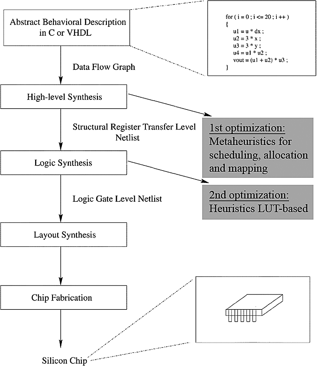
Optimization proposals in the flow of circuit implementations in FPGAs devices.
Data path algorithms can be represented using a Data Flow Graph (DFG) [31]. Each node in DFG represents an operation that is to be executed in the algorithm. High-Level Synthesis (HLS), also known as Behavioral Synthesis, is the process of converting an algorithmic description into a synthesizable Register Transfer Level (RTL) netlist. RTL is synthesized in the device with an Electronic Design Automation (EDA) tool, like the Xilinx ISE Design Suite [37] or the Vivado Design Suite [38]. The high level description may be in the form of a DFG or a programming language such as C. The HLS design flow consists of three sub-tasks; namely, scheduling, allocation and mapping [22].
The main contribution of this research is the consecutive execution of two different optimization procedures in the same project. The first optimization consists of applying multi-objective metaheuristics for scheduling, allocation and mapping, and the second optimization consists of applying an iterative technology-mapping for LUTs optimization. First, the problem is translated into a DFG. We use 6 Multi-Objective Evolutionary Algorithms (MOEAs) from the Platform Independent Interface for Search Algorithms (PISA) [5,6]. Second, the optimized schedules were converted into VHDL code using the Xilinx ISE Design Suite. The Xilinx ISE Design Suite has no updates since 2013, but it is still a widely-used software to implement FPGAs manufactured before 2013. As future work, the Vivado Design Suite will be used.
In Fig. 1 the optimization proposals for the circuit flow implementations on FPGAs devices is shown. The first optimization is in the HLS stage and the second optimization is in the Logic Synthesis stage. Before the first optimization, designs are represented using the DFGs because it is easy to manipulated them from an iterative metaheuristic algorithm and state-of-the-art methodologies exist for estimating the objective functions of interest (Delay, Area and Power).
The remainder of the paper is organized as follows. In Section 2 some previous works of the two proposed optimizations are presented. In Section 3, the definition of DFG, the Mediabench benchmark, DFG schedules and quality estimators are described. The first optimization is presented in Section 4. The second optimization process is presented in Section 5. In Section 6, the results obtained are presented. Finally, we discuss our conclusions and future work in Section 7.
Previous work on High-Level Synthesis
The use of MOEAs for optimal scheduling, allocation, and mapping in HLS has been widely reported in the literature. A framework for applying MOEA and Particle Swarm Optimization (PSO) based approaches for simultaneous Area, Delay, and Power optimization in HLS of data paths is presented in [18]. A survey of MOEAs based methodologies for HLS is presented in [22]. Evolutionary Algorithms (EAs) being population based meta-heuristics are extremely effective in design space exploration. For example, a MOEAs based methodology for data path synthesis from a DFG for multi-objective Area and Delay optimizations is described in [22]. The authors propose a multi-chromosome encoding scheme for the DFG scheduling priority and functional unit constraints. An improved low power FPGA binding of data-paths from DFG with NSGA-II based selection is presented in [19]. An extensive treatment of applications of MOEAs in Very Large Scale Integration (VLSI) and embedded systems was presented in [4].
Previous work on LUTs optimization
In order to implement a logic circuit in a FPGA, it must be converted to an equivalent one composed only of physical elements present in the FPGA, by a process called technology mapping. In some FPGAs, the main element used to implement combinational circuits is the LUT. For LUT-based FPGAs, technology mapping converts a circuit made up of gates into a circuit composed of LUTs.
There are several algorithms for this task including CutMap [10], DAOMap [9] and ZMap [11]. The IMap algorithm [28] is used to perform technology mapping with the objective of minimizing the number of LUTs generating smaller solutions and faster runtimes in comparison with FlowMap, CutMap, DAOMap and ZMap.
These two areas of research exist separately: MOEAs for HLS and LUTs optimization. However, no research has been reported in the literature that applies both optimizations consecutively.
Background
Data Flow Graph
A DFG represents a design in HLS, an instruction set that must run sequentially or in parallel to achieve the required results [34]. Each graph node is a contiguous code region without branches and the edges between nodes indicate jumps in the program flow. The node function generates a new value on its outputs, depending of its inputs. Formally, a DFG is defined as
The nodes represent operations in a DFG. A directed edge
Mediabench benchmark
The Mediabench benchmark [26,27] was used to perform and validate the experiments to optimize the DFG and then convert to VHDL code, which can be synthesizable in FPGA devices. The Mediabench benchmark was selected because it is widely used in the literature [4,18,19,22,36].
Mediabench has a base of 20 accessible circuits in .dot format with a directed graph structure. With an algorithm written in C language, the conversion from .dot format to a graphs format .graphml (standard graph format written in xml) was performed. Being the DFG in .graphml format already, they can be charted and analyzed with the yEd tool [39]. In addition, being the DFG in standard .xml format, it is possible to read it with the C language library pugixml [21].
The experiments were performed with 10 circuits of the benchmark and the features of each DFG (number of nodes, number of edges and number of operations) are detailed in Table 1.
Features of the DFG Mediabench benchmark
Features of the DFG Mediabench benchmark
For DFG scheduling it is necessary to have a way to encode. There are two main elements [18,19,22]:
Node priority field: used to encode a topologically sorted permuted list of tasks (nodes).
Module allocation field: consists of a list of integers specifying the maximum number of functional units of each type available for scheduling in every clock cycle.
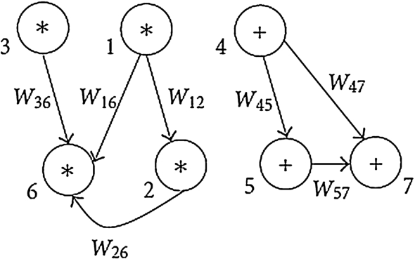
In Fig. 2 a DFG example with the Node priority field is shown, that requires to first run node 3, then node 1, and so on until node 7. In the Module allocation field there are functional units (two multipliers and one adder). Note that in Fig. 3, the DFG is scheduled in clock cycles defined by the functional units availability, in accordance with the node dependencies in the DFG. In first clock cycle multiplication operations 3 and 1 should be executed. It can be seen that the operation 2 should be run on the second clock cycle because the operations 3 and 1 are occupied, the 2 functional units are available in multiplication restrictions of the Module allocation field. The following are basic schedulings that can be applied to the DFGs.
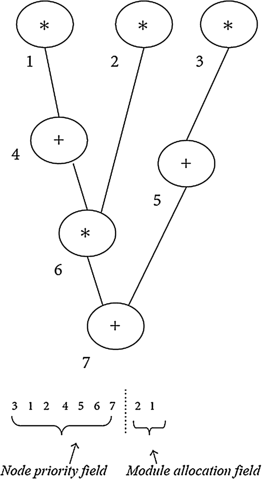
Example of a schedule for DFG.
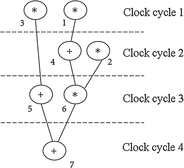
Clock cycles for a DFG scheduling.
Basic schedulings represent the simplest ways to define the schedule. It is assumed that the number of functional units has been previously specified and the operations in the graph are sorted with respect to their data dependency. The resulting scheduling may not be optimal, but results obtained with As Soon As Posible (ASAP) and As Late As Posible (ALAP) are fastest. Three basic schedulings were implemented:
ASAP: The simplest type of scheduling occurs when we wish to optimize the overall latency of the computation and do not care about the number of resources required. This can be achieved by simply starting each operation in a DFG as soon as its predecessors have completed [12].
ALAP: It is a variant of ASAP, but postpones the execution of nodes without affecting the amount of total clock cycles needed to fully implement the DFG. Each node is executed in the clock cycle as late as possible.
Random: As the name suggests, it is a scheduling where nodes are assigned to functional units randomly, without violating the dependency in the DFG.
Implementations of ASAP and ALAP do not have Area restrictions. This means that they use the functional units necessary to carry out operations as soon as possible or as late as possible, respectively. For this reason, the two implementations consume many functional units (Area) and power consumption (Power). An example is shown in Fig. 4 [34], where ASAP in the first clock cycle needs 5 functional units and ALAP in the third clock cycle requires 4 functional units. These two designs always produce schedules with the fewest clock cycles possible to execute the entire DFG.
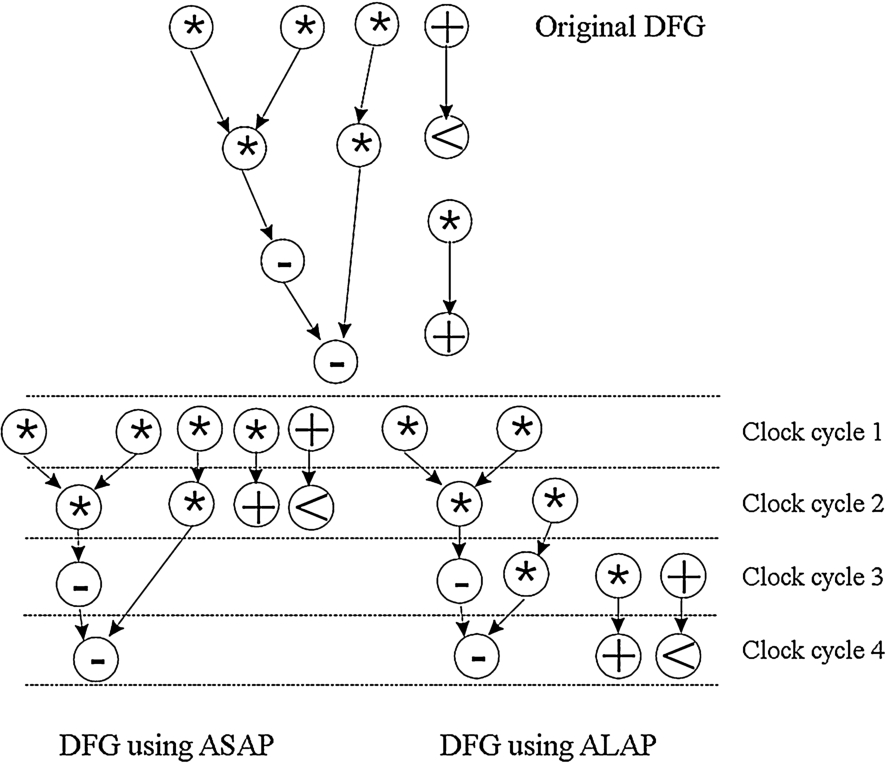
Example of basic scheduling, with ASAP and ALAP made on a DFG.
Schedules are subject to three estimates to measure their quality and thus make comparisons. These estimates are proposed in [18,22,23].
Delay: The Delay or length L is the number of time steps or clock cycles needed to run the DFG scheduling. In the example of Fig. 3, the Delay is 4 because 4 clock cycles are sufficient to compute the DFG. Area: The cost of Area (A) of a design is based on the total of Functional Units ( Power: To estimate Power, first a compatibility graph is created. Where a node i is connected to another node j, if the operation of node j can be executed in the same FU of node i. To do this, they need to have the same kind of operation and their variables cannot overlap in time. An example of a compatibility graph is shown in Fig. 5, the example corresponds to the DFG of Fig. 3 [18]. The estimation Power (P) based on is given by
Example of a compatibility graph.
The problem of finding an ideal scheduling, allocation and mapping is NP-hard [35]. Hence, metaheuristic algorithms are needed to solve it. First, tests are done to determine if the three performance measures define conflicting objectives.
HLS as a multi-objective problem
In order to evaluate whether the problem is multi-objective, it is necessary to use the payoff matrix [29]. The payoff matrix is a matrix that allows us to quantify the level of conflict between the objectives being considered. It is constructed from the solutions obtained after optimizing each objective independently. The payoff matrix is a square matrix where the diagonal is the ideal point, formed by the optimal values of each objectives. The payoff matrices of 10 DFGs of the benchmark are detailed in Table 2, where it can be seen that the three objective functions are opposed notably. Diagonals are marked in bold. We run 10 times each uni-objective algorithm: ASAP basic scheduling, uni-objective EA only optimizing Area and uni-objective EA only optimizing Power. We select the best solution for each objective. The basic scheduling ASAP always achieves the best value for the objective function Delay.
Payoff matrices of 10 DFG of the Mediabench benchmark
Payoff matrices of 10 DFG of the Mediabench benchmark
Based on the results in Table 2, multi-objective algorithms for this problem are required. A MOEA achieves a balance of 2 o more objectives functions without preferring neither of them. A complete review of these techniques is beyond the scope of this work, the interested reader is referred to [4,13,24,33,40].
For the experiments of MOEAs the PISA [5,6] framework is used. This platform is based on separating the optimization process in two parts: the optimization problem and the selection process. We evaluate 6 different selection processes in PISA:
Nondominated Sorting Genetic Algorithm II (NSGA-II) [14,15].
Fair Evolutionary Multi-objective Optimizer (FEMO) [25].
Hypervolume based multi-objective Evolutionary algorithm (HypE) [3].
Indicator-Based multi-objective Evolutionary Algorithm (IBEA) [41].
Strength Pareto Evolutionary Algorithm 2 (SPEA2) [42].
Weight Sum vector Genetic Algorithm (WSGA) [22].
After performing the optimizations, the occupied Areas are calculated and compared by EDA tools such as the Xilinx ISE Design Suite, these tools are important because with them VHDL codes can be implemented in real devices. This is another contribution of this research, because in the state-of-the-art, implementations are usually not reported with EDA tools.
When measuring the quality of multi-objective algorithms two aspects are generally taken into account: minimize the distance of the obtained solutions by the algorithm, regarding the optimal Pareto Front (PF) [33] of the problem; and maximize the spread of solutions on the front so the distribution is as uniform as possible. However, since the optimal PF in unknown, several quality indicators are used to measure the performance of the algorithms; these are:
Epsilon: It is the most used indicator because it measures the distance or difference between PF and approximate best known front, so it gives a clear and direct idea of performance. This indicator should be minimized and is based on a ratio of ε-dominance. There is a multiplicative version and a additive version of this indicator [43]. Hypervolume: This indicator, proposed in [3], measures the Hypervolume of one portion of space that is weakly dominated by a set approach A, and it is maximized. It measures the convergence and the diversity jointly. In order to calculate this value, the objective space must be defined by a reference point that dominates (at least weakly) all the points to be used. R: This indicator can be used to evaluate and compare sets of approaches based on a set of utility functions. This indicator should be minimized. A utility function is defined as a representation from the set of target vectors n-dimensional to a set of real numbers [17].
Second optimization process: LUTs optimization
This section describes the second optimization, but first, it is necessary to convert the scheduled DFG to VHDL code. This is important because it allows comparing the estimates made on the DFG versus the actual estimates made by tools such as the Xilinx ISE Design Suite. The VHDL code is converted into Moore Finite States Machine (FSM) [30]. Already having the VHDL code optimized in a Moore FSM, these may be subjected to a second optimization phase, in the Logic Synthesis stage.
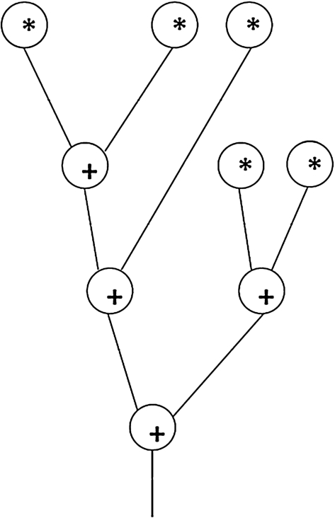
DFG example with two types of operations (adders and multipliers).
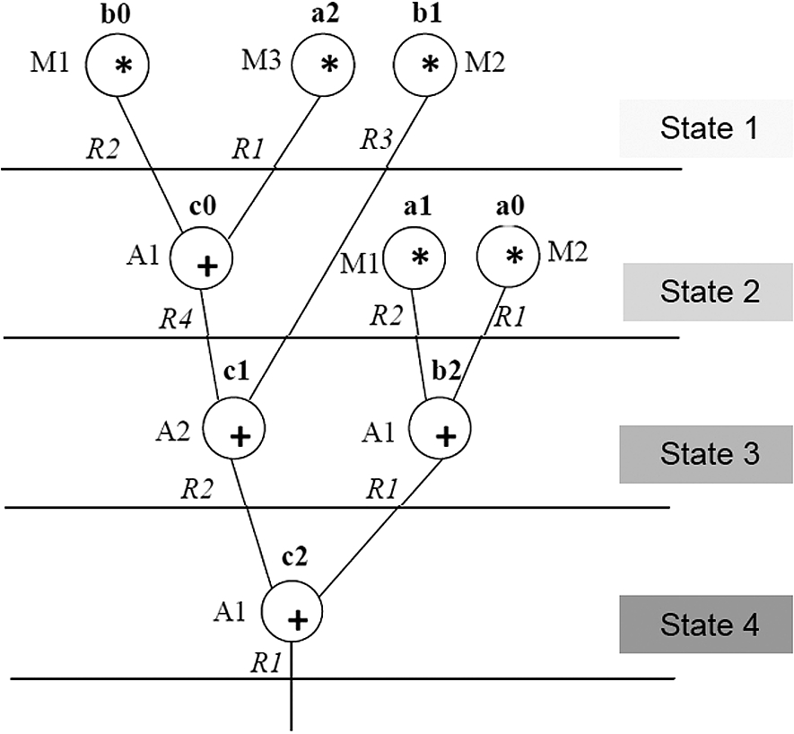
Example distribution of states for a DFG schedule.
VHDL code generation takes place as follows. Once the DFG is read in format .graphml with pugixml, this generation is done in C code. VHDL code is automatically generated from the DFG schedule detailed in Section 3.3. For getting the VHDL code type Moore FSM, we included in the architecture definition the sentences CASE IS WHEN for each state of FSM. Each state is equivalent to a planned clock cycle, as it is shown by examples in Fig. 6 and Fig. 7; where R1, R2 and R3 represent records for storing the outputs of operations; A1, A2, M1, M2 and M3 represent functional units (of addition and multiplication); and a0, a1, a2, b0, b1, b2, c0, c1 and c2 are the node operations [19]. The state diagram for this example is shown in Fig. 8. If all states were executed, all output signals have definite values.
The results of each operation in the state are stored in registers, and are shared global variables. The inputs and outputs of the Entity – part of the VHDL code – are defined like data type unsigned of 4 bits and 5 bits, respectively, with the library IEEE.NUMERIC_STD, in order to carry out all necessary operations (adder, multiplier, exponential and so on). However, the number of bits of inputs and outputs can be defined differently. In addition, in the entity, reset and the clock are input ports. The VHDL architecture has two processes: one to change from one state to another, which only runs if there is a change in the inputs reset or clock; and another process, that has as sensitive list the signal representing the current state. This second process contains the combinational logic of all states.
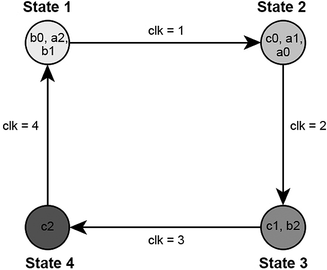
State diagram for a DFG schedule.
After performing conversions into VHDL code, it is necessary to validate the syntax and logic with a corresponding EDA tool. In this case it was validated with the Xilinx ISE Design Suite (Version 14.7) [37]. Simulations of the 10 benchmark circuits were performed with the 3 basic schedules explained in Section 3.4. All simulations were performed on the FPGA Xilinx Spartan 3E XC3S500E device, and FG320 package.
Iterative technology-mapping algorithm
The technology mapping of the benchmark circuits was performed using the IMap algorithm [28]. This iterative algorithm is reviewed here. Some circuits in the benchmarks contain sequential logic. IMap was applied only to the combinational portion of these circuits.
Overview
IMap takes a circuit composed of simple gates and converts it into a circuit composed of LUTs. These circuits are represented as Directed Acyclic Graphs (DAG), defined as
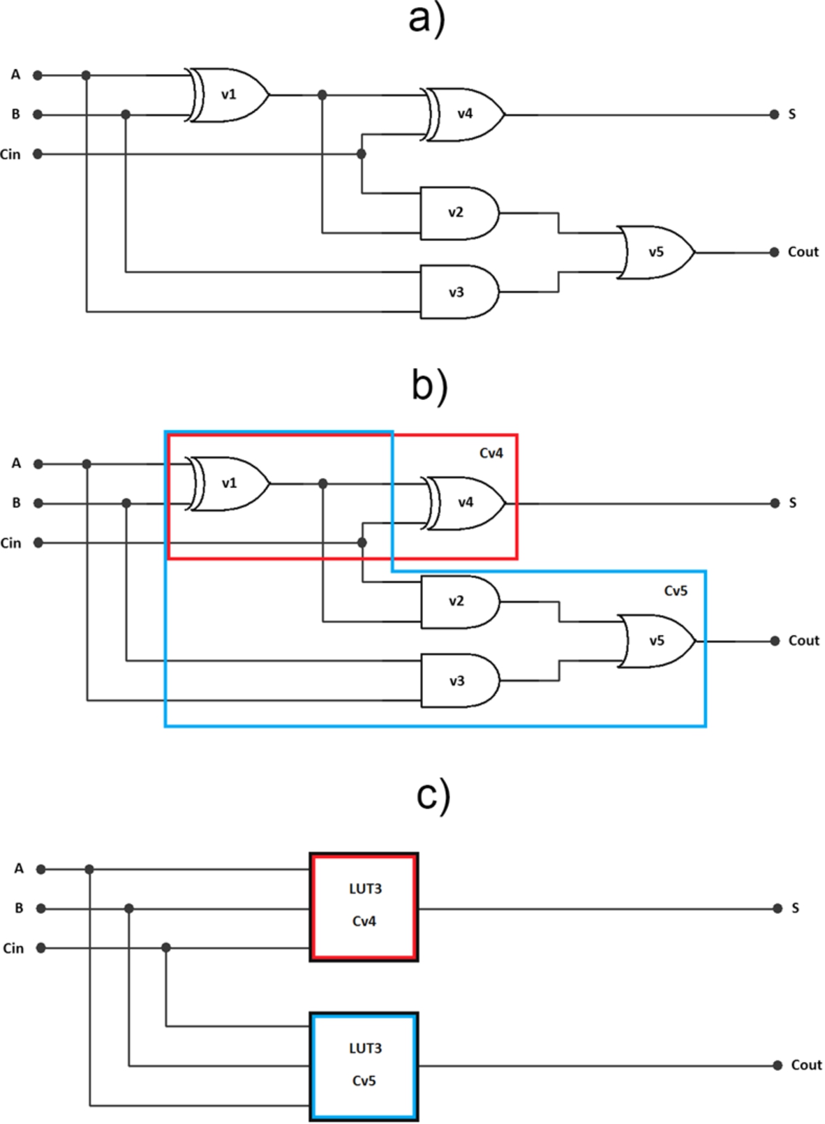
Technology mapping with IMAP of combinational circuit full adder. (a) Original circuit. (b) Best cones. (c) Equivalent circuit with LUTs.
Forward traversal selects the best cone for every node. A following backward traversal selects a set of cones to cover the whole graph. Iteration is beneficial because every backward traversal influences the behavior of the next forward traversal. Finally the cones selected by the final backward traversal are converted into LUTs [28]. Following are more details on each step (Generation of K-feasible cones, Forward traversal, Backward traversal and Conversion of cones into LUTs).
The mapping of a circuit is done using cones. A cone
Forward traversal
For each node the best cone is selected. This selection determines the quality of the mapping solution. Cones can be selected to either minimize depth or minimize Area. Selecting the cone that minimizes depth at each node leads to a mapping solution that is depth optimal. To minimize Area the Area flow metaheuristic is used. The Area flow of each cone is computed and the cone with the lowest Area flow is selected. However, the value of the Area flow depends on the number of output edges of the cone, which cannot be known until the backward traversal selects the cones to cover the whole graph. Therefore, an approximation that improves with the number of iterations is used [28]. All the benchmark circuits were mapped to minimize Area.
Backward traversal
The graph is traversed in reverse topological order from PO to PI. At each node the best cone selected by the preceding Forward traversal (see Section 5.6) is used. The nodes covered by a previously used cone are skipped so that only the nodes that are required to be visible are expanded. The cones selected by the backward traversal cover the whole graph and compose the mapping solution [28].
In Fig. 10 to Fig. 12 IMap is applied to a small example circuit. A mapping solution for this circuit with
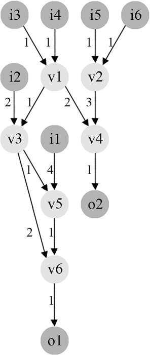
Original circuit. IMap applied to example circuit.
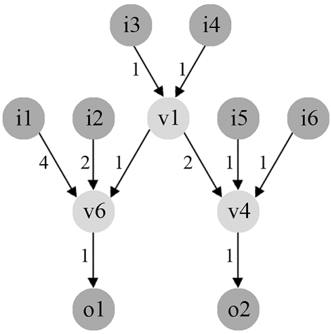
Example circuit to which IMap is applied, using
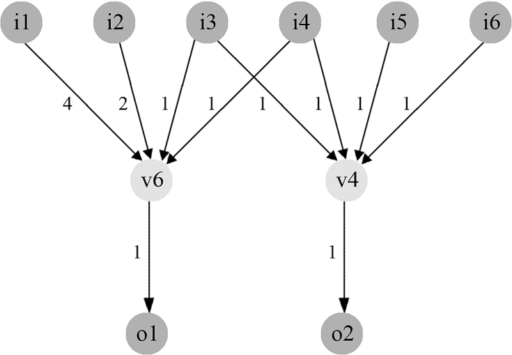
Example circuit to which IMap is applied, using
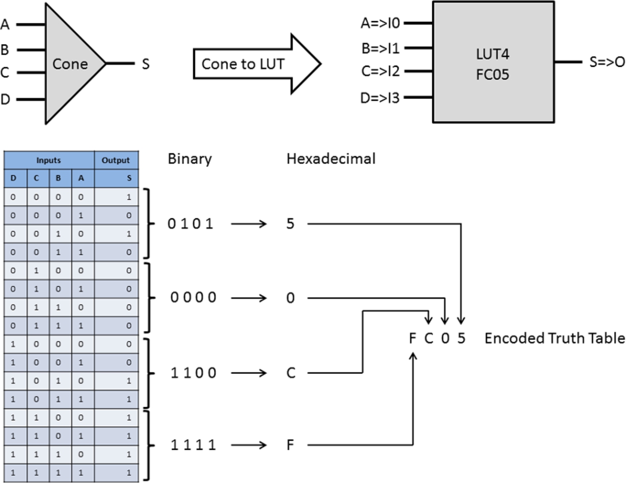
Conversion of a cone into a LUT.
Each cone in the mapping solution is converted into a LUT that implements the functionality of the cone. These LUTs are defined by a string of hexadecimal digits which encode the truth table of each cone. An example of how this conversion is done is shown in Fig. 13.
Results
This section presents the experimental results. In the first optimization process, the comparative results of the MOEAs through quality indicators are presented. Subsequently the results achieved on the 3 objective functions are presented. Also, the Area estimates made in simulation with the Xilinx ISE Design Suite are presented. In the second optimization process, a comparison between the estimates made in simulation with the Xilinx ISE Design Suite and results of Area minimization in LUT-based FPGA technology mapping are presented.
Results of the first optimization process
The MOEAs experimental parameters are composed by the Table 3.
The MOEAs experimental parameters
The MOEAs experimental parameters
Results for the Epsilon indicator, showing the average value of all runs; bold indicates the best
Results for the Hypervolume indicator, showing the average value of all runs; bold indicates the best
Table 4, Table 5 and Table 6 show the quality indicators of 6 MOEAs with 10 DFG of the Mediabench benchmark. In bold is the best result for each problem.
It can be seen that the WSGA metaheuristic achieves results with less quality, according to three quality indicators. Although, SPEA2 and NSGA-II achieve results with slightly higher quality than the other metaheuristics. SPEA2 and NSGA-II achieve the best results eight times and eleven respectively.
The NSGA-II algorithm has a better performance than the WSGA algorithm, this behavior is similar to the results reported in [18].
On the other hand, results of Table 4, Table 5 and Table 6 are not compared with [18], because quality indicators (Epsilon, Hypervolume and R) are not reported in [18].
As a second set of results to be analyzed we report the values of the objective functions in the PF found. The objective functions average of all individuals of the PF is calculated. For this, the six MOEAs are compared with the 3 basic scheduling algorithms. Next tables show the performance of 6 MOEAs with 10 DFG of the Mediabench benchmark. Table 7 shows the average of the Delay objective function, Table 8 shows the average of the Area objective function and Table 9 shows the average of the Power objective function. Table 10 show the improvement for each problem of Area and Power with respect to the basic scheduling algorithms. In each table, the best result is indicated in bold.
In the case of Delay, there is not improvement by any of the metaheuristics, this is because the basic scheduling algorithms, ASAP and ALAP, always give the minimum clock cycles possible. However, an average improvement of 14.06% is obtained in terms of the Area and 7.01% in terms of Power.
Analyzing the diversity of the obtained solutions, the PF found by NSGA-II has higher diversity than the other algorithms. In Fig. 14, NSGA-II for one of the problems (EWF) is shown.
Results for the R indicator, showing the average value of all runs; bold indicates the best
Results for the Delay objective function, showing the average value of all PF individuals; bold indicates the best
Results for the Area objective function, showing the average value of all PF individuals; bold indicates the best
Results for the Power objective function, showing the average value of all PF individuals; bold indicates the best
Improvement of Area and Power respect basic scheduling algorithms
In Fig. 15 is shown the runtimes for the EWF problem in Intel Xeon CPU 2.80 GHz and RAM memory of 8.00 Gb.
The schedules are converted into VHDL code, these codes were estimated in terms of Area with the Xilinx ISE Design Suite. Comparisons of the six MOEAs were performed with the three basic scheduling algorithms, in order to measure whether the improvements achieved with the DFG estimates are similar to those calculated by the Xilinx ISE Design Suite. Table 11 shows the results regarding the Area occupied given by Slice Registers (FlipFlops + Latches). No data is presented in the case of ALAP with MESA-HB because the Xilinx ISE Design Suite marks an error. Bold is the best result for each problem.
An average improvement of 14.95% is obtained in Area. The reduction achieved with DFG estimators is similar to what is calculated by the Xilinx ISE Design Suite. Each PF contains a set of individuals and it is necessary that one of them is selected to be submitted to the next optimization stage. For this reason, an individual was randomly selected from each PF.
The optimized VHDL code was implemented with the Xilinx ISE Design Suite. The resulting netlist is exported to edif format and imported into Matlab with the help of the BYU EDIF tool [7]. The circuit is converted into simple gates and simplified using the ABC tool [1]. Circuit exchange between ABC and Matlab is performed using the aiger format [2]. Then technology mapping with IMap is performed and the mapping solution is exported to edif format. Finally, edif format is imported to the Xilinx ISE Design Suite for further testing. In Fig. 16 an example of a simulation with the Xilinx ISE Design Suite is observed corresponding to the MESA-FP problem with IBEA. Then, in Fig. 17 is presented the simulation of IBEA optimized and LUT optimized in the same problem. It can seen that both have the same behavior.
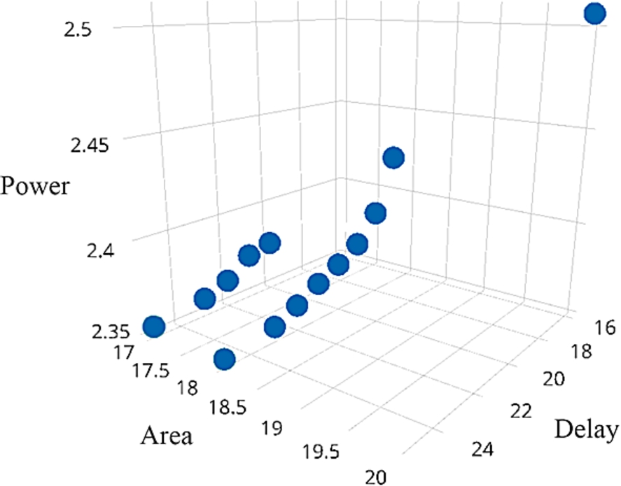
Example of PF obtained by NSGA-II for EWF problem.
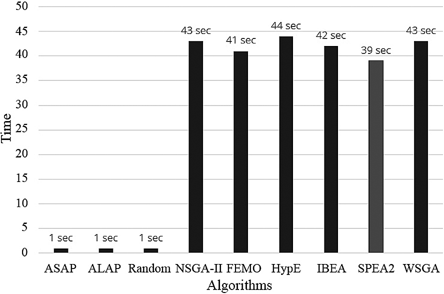
Time (in seconds) measurements for the EWF circuit (34 nodes).
Results of Area Slice Registers (FlipFlops + Latches)
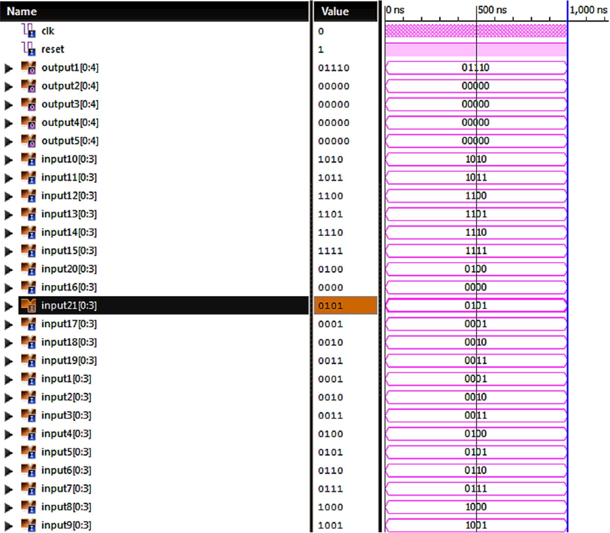
Simulation of IBEA optimized MESA-FP circuit.
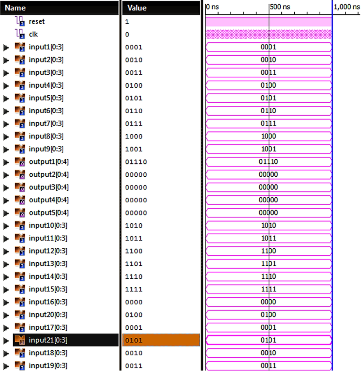
Simulation of IBEA optimized and LUT optimized MESA-FP circuit.
Next, we present results of applying the LUTs optimization on 10 benchmark problems in Table 12, Table 13, Table 14, Table 15, Table 16, Table 17, Table 18, Table 19, Table 20 and Table 21. Bold values means a decreased amount of LUTs relative to the original circuit. In each table, a different problem is presented. Each row of the tables represents a circuit in VHDL code generated automatically after the first optimization process, corresponding to the six MOEAs applied. The original and the optimized columns represent the amount of LUTs estimated for each circuit by the Xilinx ISE Design Suite. The other two columns represent the difference of the LUTs amount and the average improvement of the circuit optimized with respect to the original version (without LUTs optimization).
The results show that the process obtains a 60% reduction of total circuits with LUTs occupied, compared with the results obtained with the Xilinx ISE Design Suite.
Applying two consecutive optimizations in circuit design for FPGA devices can be advantageous. As a first optimization, we apply several MOEAs for the HLS stage. As the second optimization, we realize reductions of LUTs in Logic Synthesis stage using the IMap algorithm. In the first optimization, it is feasible to use MOEAs to find better schedules than the basic schedules. With an average improvement of 14.06% in terms of Area occupied and 7.01% in terms of Power consumption. Furthermore, it was observed that the quality of obtained solutions for each metaheuristic algorithm is similar. Although it is important to note SPEA2 and NSGA-II are better in comparison with the rest of the algorithms. The WSGA algorithm has a weak selection process (uni-objective) and does not achieves the quality of the other algorithms. In the second optimization, the results of Area minimization in LUT-based FPGA technology mapping was positive. Results obtained a 60% of the circuits with reduction in the amount of LUTs occupied, compared with the Xilinx ISE Design Suite. The ARF problem is an example of the effectiveness of applying both optimizations consecutively. Initially, when ARF is optimized by the MOEA-FEMO, 14.63% reduction in terms of Slice Registers (FlipFlops + Latches) is obtained. Then, when ARF is optimized by the IMap algorithm, 6.99% reduction in terms of LUTs is obtained.
In future work, we want to measure the search operators (crossover and mutation) to determine if they are suitable for such problems or if better search operators can be applied. Also, parallelization of the optimizations should reduce runtimes. Besides, we are interested to review other approaches for estimating the objective functions. In addition, we want to do the experiments with the Xilinx Vivado Design Suite and we want to evaluate our approach on several FPGA devices.
LUTs optimization on HAL problem
LUTs optimization on MESA-HB problem
LUTs optimization on ARF problem
LUTs optimization on MPEG-MV problem
LUTs optimization on EWF problem
LUTs optimization on FIR2 problem
LUTs optimization on FIR1 problem
LUTs optimization on JPEG-SD problem
LUTs optimization on MESA-PF problem
LUTs optimization on EPIC problem
Footnotes
Acknowledgements
The authors acknowledge the support of CONACYT, PRODEP with the project ITTIJ-PTC-007, Tecnológico Nacional de México with the project 5861.16-P and CONACYT with the project No. 9444, Aprendizaje evolutivo a gran escala, Fronteras de la Ciencia 2015-2.