
Abstract
In this work, we investigate the effect of the carrier gas (iodine) utilisation conditions on the growth of CuInSe2 (CIS) thin films deposited by the close spaced vapour transport technique. This study shows that the CIS films deposited at 430°C, with heated iodine and open reactor, are of high quality in structural, optical and electrical properties. Analysis by X-ray diffraction showed that these films are polycrystalline and have a chalcopyrite structure. The preferential orientation according to the plane (112) was obtained. The morphological study of these films showed that they present a compact aspect with crystallites of uniform size. The energy dispersive spectrometer analysis showed that these films are slightly copper rich. The optical and electrical studies at room temperature gave the following results: an energy gap of 1 eV, an absorption coefficient higher than 105 cm− 1, p type conductivity and a low resistivity of 0·12 Ω cm.
Introduction
Solar cells based on chalcopyrite structure materials as absorber layers are attracting a great deal of attention.1–7 These materials have a high absorption coefficient and a low fabrication cost. The solar cells having Cu (In, Ga) Se2 absorbers have reached efficiency over 20%. 8
A variety of methods including co-evaporation, 9 electrodeposition, 10 thermal evaporation, 11 sputtering, 12 spray pyrolysis, 13 flash evaporation 14 and close spaced vapour transport (CSVT) 15 have been reported for the formation of CuInSe2 (CIS) thin films. Many of these technologies require the use of vacuum and heat treatment operations, which contribute to the increase of production costs of the prepared samples. In order to obtain competitive CIS thin films, a simple system of CSVT technique was used without vacuum. More additional heat treatments were not necessary. In the framework of this study, we investigate the effect of the carrier gas (iodine) utilisation conditions on the growth of CIS thin films deposited by CSVT.
Experimental
CIS thin films were deposited on Pyrex substrates using a vapour transport system at short distance (CSVT). Unlike other CSVT systems that use vacuum 15 in order to deposit thin films, in the case of this work, a continuous sweeping of the deposition system by a stream of argon before and during the growth phase is enough. As shown in Fig. 1, the used CSVT system consists of two lids and a main quartz tube having a length of 40 cm and an inner diameter of 3·5 cm. The lid of the entry has two inlets with valves, which are used to control the sweeping speed of the reactor under a stream of argon, with or without iodine. The second cover has an output with valve for venting to the outside. To minimise the loss of temperature, the main vessel of the reactor is surrounded by refractory bricks. The used Pyrex substrates are flat, polished, well cleaned and thoroughly dried. The source material is a powder of CIS placed in a graphite crucible. This powder is obtained from an ingot of CIS, which was prepared by the vertical Bridgman method, 16 with elements having purities of 99·999% for Cu, In and 99·9999% for Se. The substrate is placed above the crucible on 1 mm thick Pyrex blocks. The assembly is placed in the middle of the reactor. A few grains of solid iodine are placed either in inside position or in outside position. A ‘U’ Kanthal bar under the reactor, just below the source, provides the heating (source and substrate). As mentioned in Table 1, the substrate temperature was maintained at 430°C for a duration of 1 h. Heating coils are used for rising the iodine temperature. The chemical reactions involved in the preparation of CIS films have been reported by many authors.15,17
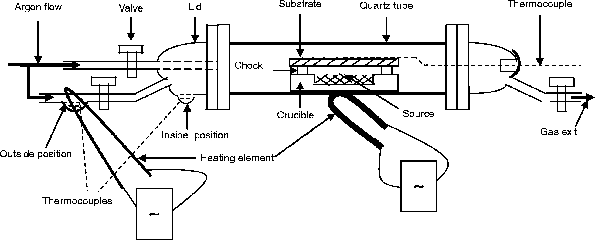
Schematic diagram of CSVT reactor
Deposition conditions
A scanning electron microscope (SEM), associated with an energy dispersive spectrometer (EDS), was used to study the morphology of the film surface and determine the chemical composition of their constituents. An X-ray diffractometer (XRD) with Cu Kα radiation (λ = 1·54051 Å) was used to analyse the crystal structure of CIS deposited films and determine the different crystallisation planes and the various existing phases. A UV–Vis–NIR (near infrared) spectrophotometer was used to measure the transmittance at room temperature in order to obtain the absorption coefficient and the band gap value of the prepared compound. The electrical properties were carried out using an HMS-3000 Hall measurements system.
Results and discussion
Compositional analysis
CIS thin films prepared by the CSVT technique were characterised by EDS, and the results are displayed in Table 2. The chemical composition of the constituents is obtained after analysis of five different locations of each studied film.
Chemical composition of CIS samples determined by EDS
Sample CIS 1 prepared at 430°C, in a closed reactor, has a high iodine proportion, which is near 40 at-%. For samples CIS 2 and CIS 3, the amount of iodine is reduced to < 4 at-% for CIS 2 and falls below 1 at-% for CIS 3. The comparison of the chemical compositions of samples CIS 2 and CIS 3 shows that the amount of iodine is lower in films deposited under heated iodine. In other words, when iodine is heated, it contaminates less the deposited CIS films. Meeder et al. 18 showed that the film surface of the ternary CGS deposited by the chemical vapour deposition method and two-stage open tube may be contaminated with iodine as transport agent used in the process of film growth. The presence of iodine is more pronounced in the copper rich films. 19 This is consistent with the obtained results, which showed that when the films are more rich in copper, the contamination by iodine is more important. The EDS analysis showed the quasi-stoichiometry of the CIS 3 film, with a Cu/In ratio of 1·03.
Surface morphology
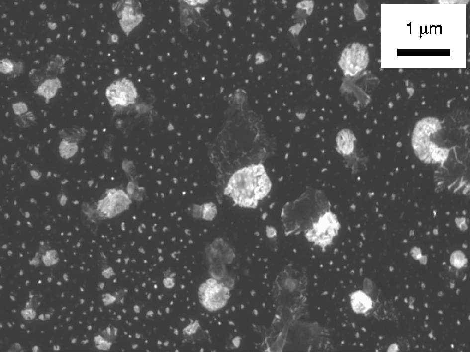
The SEM image of CIS 1 is shown in Fig. 2. In this figure, the contamination of the film by iodine appears as large white patches. Analysis by SEM of samples CIS 2 and CIS 3 showed that these films consist of crystallites of uniform size, as shown in Figs. 3 and 4. Unlike CIS 2, which is less filled in crystallite, sample CIS 3 presents a more compact aspect with an average grains size of ∼0·3 μm. This value is in good agreement with that reported by Fan et al. 20 In these figures, we note the absence of iodine patches. This confirms the obtained EDS results that are listed in Table 2, which indicate a low contamination of films CIS 2 and CIS 3 by iodine. The Cu/In ratio of >1 shows that CIS 3 is slightly copper rich. Menna et al. 21 showed that the films with a Cu/In ratio of >1 are desirable for good photovoltaic conversion efficiency.
SEM image of CIS 1
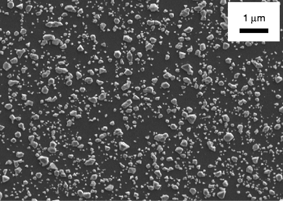
SEM image of CIS 2
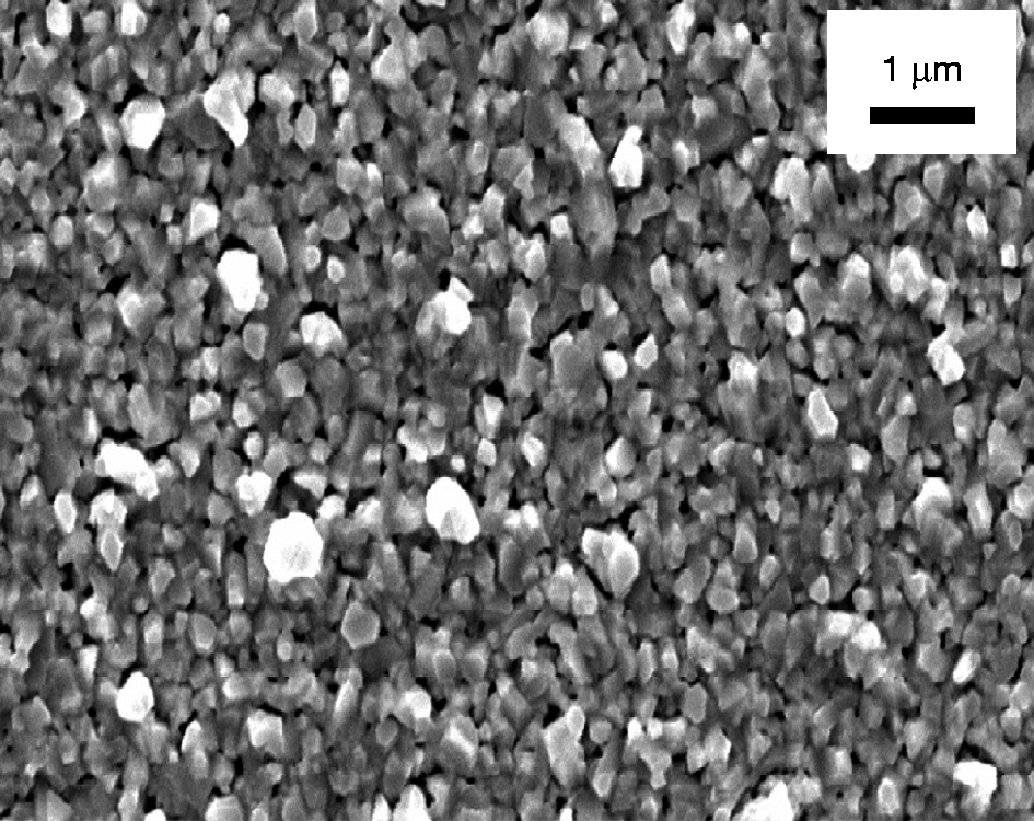
SEM image of CIS 3
Structural analysis
The results of the characterisation by X-ray diffraction of CIS films, deposited at a substrate temperature of 430°C for 1 h and under different operating conditions of the carrier gas, are presented in Figs. 5–7.
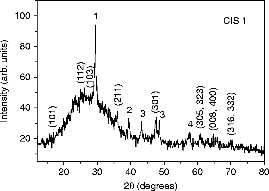
XRD pattern of CIS 1: 1, CuI; 2, In6Se7; 3, Cu2Se; 4, CuSe2
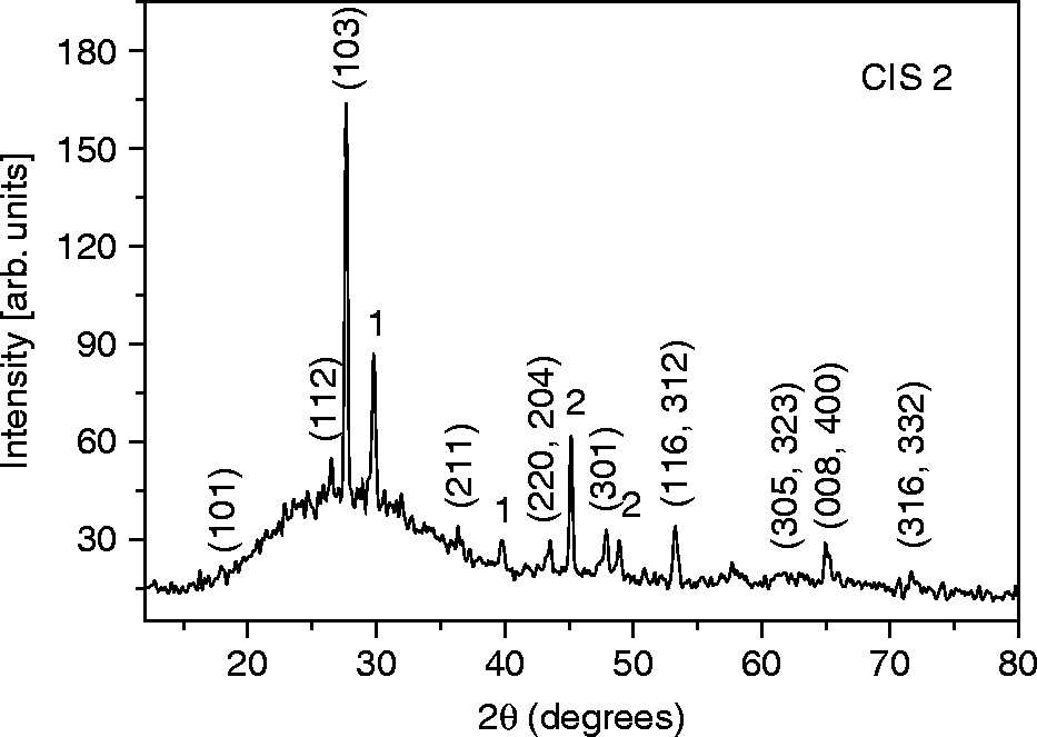
XRD pattern of CIS 2: 1, In6Se7; 2, Cu2Se
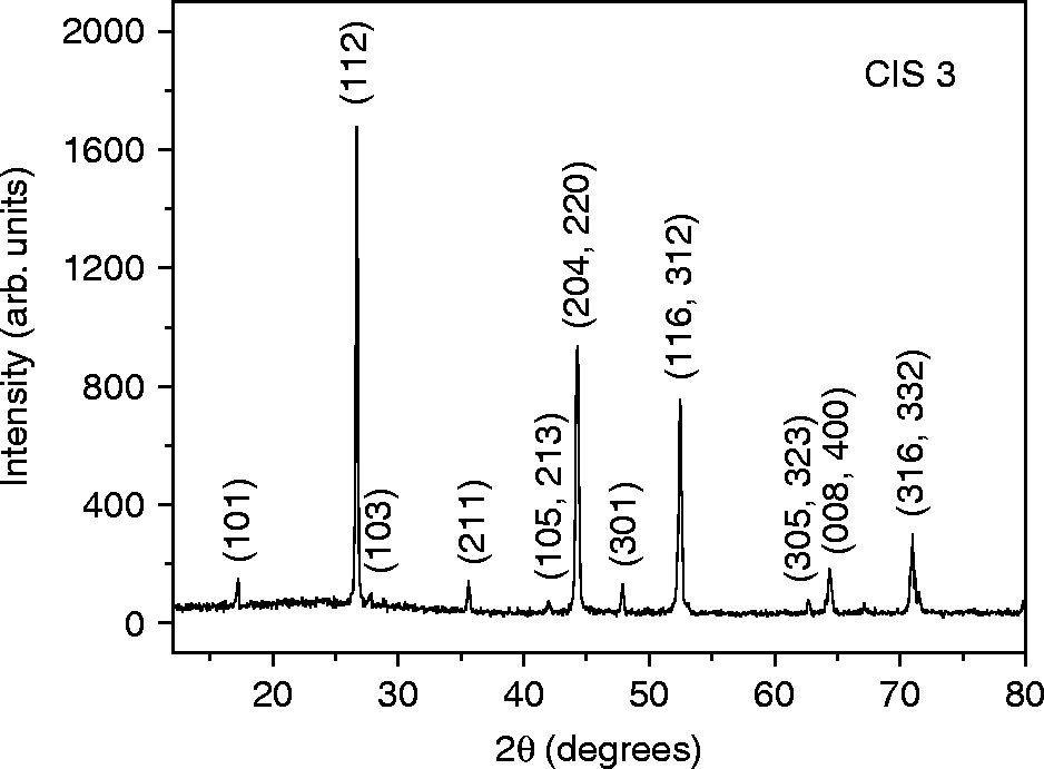
XRD pattern of CIS 3
The spectrum in Fig. 5 shows that the peak characterising the binary phase CuI is dominant for the deposited layer in a closed reactor with the iodine inside the reactor. For samples CIS 2 and CIS 3, we note the disappearance of the phase CuI, as illustrated in Figs. 6 and 7. Furthermore, Fig. 6 shows that the planes of orientation (112), (204/220) and (116/312) have a very low intensity for the films deposited in an open reactor with unheated iodine. On the other hand, the deposited film in an open reactor with heated iodine shows an intensity increase for the peaks (112), (204/220) and (116/312) with a preferential orientation according to the direction (112), as shown in Fig. 7. Similar results were reported by other authors.15,22
In addition to the planes of orientation (112), (204/220), (116/312), (305/323), (008/400) and (316/332) of the CIS ternary compound, most characteristic peaks of the chalcopyrite structure (101), (103), (211), (105/213) and (301) are shown by the spectrum of sample CIS 3.
The lattice parameters a and c for the CIS 3 film were determined using Bragg's law. 23 The obtained results shown in Table 3 are in good agreement with literature. 24
Lattice parameters of sample CIS 3
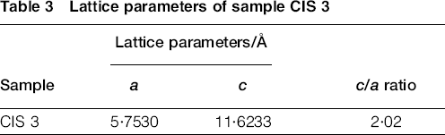
The presence of the characteristic peaks of the chalcopyrite structure and the ratio of the lattice parameters c/a ≈ 2 show that sample CIS 3 has a chalcopyrite structure.
Gap determination
Figure 8 depicts the variation of (αhν)2 versus photon energy (hν) of sample CIS 3 prepared in the framework of this study. The absorption coefficient α was calculated from the experimentally measured transmittance of sample CIS 3, and the obtained value of α was found to be higher than 105 cm− 1.
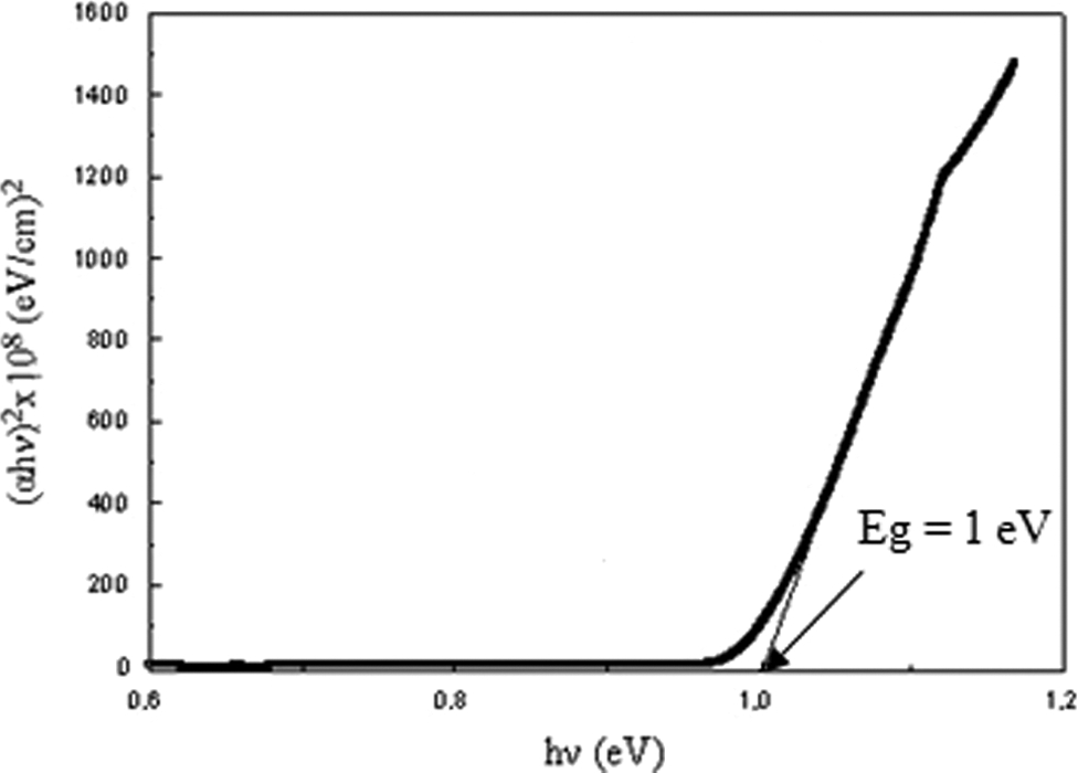
Plot of (αhν)2 versus photon energy (hν) of CIS 3
From the characteristic (αhν)2 versus photon energy (hν), we determine the value of the energy gap of the compound. For the CIS, which is a direct gap semiconductor, the absorption coefficient is given by the following equation: 25 α = (A(hν − Eg)1/2)/hν, where Eg is the energy gap, A is a constant, ν is the frequency of the radiation and h is the Planck constant. The energy gap is determined by extrapolating the linear part of the curve (αhν)2 versus (hν) to the intersection with the x axis, or (αhν)2 = 0, so Eg = hν. As shown in Fig. 8, we find that the optical energy gap of the prepared material is Eg = 1 eV. This value is in good agreement with those reported elsewhere.26,27
Electrical properties
The electrical properties of CIS thin films are required for the optimisation of the preparation conditions to use it as an absorber in solar cell. 28 Measurements of the Hall effect and the resistivity were carried out at room temperature on the CIS 3 film. The obtained positive Hall voltage indicates that the prepared film is of p type nature with holes as majority charge carriers. In addition, the obtained values of resistivity, Hall mobility and carrier concentration are 0·12 Ω cm, 65·1 cm2 (V s)− 1 and 8 × 10 17 cm− 3 respectively. Similar results were reported by Shah et al. 14
Conclusion
CIS thin films were deposited using the CSVT method. The film deposited in a closed reactor is heavily contaminated by iodine, whereas the film prepared with unheated iodine has its crystallites very weakly packed. Alone, the CIS 3 film deposited in an open reactor and heated iodine has been found very lightly contaminated with iodine and better filled by crystallites. Furthermore, the EDS analysis showed the quasi-stoichiometry of the CIS 3 film, with a Cu/In ratio of 1·03. Structural studies of this sample have shown its polycrystalline state and its chalcopyrite structure. The preferential orientation according to the plane (112) was obtained. The gap width of this film was found to be equal to 1 eV at room temperature. Its absorption coefficient is higher than 105 cm− 1. In addition, this film presents p type conductivity and a low resistivity of 0·12 Ω cm. Thus, the structural, optical and electrical characteristics of CIS 3 show that this film is an appropriate material for photovoltaic applications.